Abstract
This paper investigates the impacts of post-rapid thermal anneal (RTA) and thickness of ZrO2 on the polarization P and electrical characteristics of TaN/ZrO2/Ge capacitors and FeFETs, respectively. After the RTA ranging from 350 to 500 °C, TaN/ZrO2/Ge capacitors with 2.5 and 4 nm-thick amorphous ZrO2 film exhibit the stable P. It is proposed that the ferroelectric behavior originates from the migration of the voltage-driven dipoles formed by the oxygen vacancies and negative charges. FeFETs with 2.5 nm, 4 nm, and 9 nm ZrO2 demonstrate the decent memory window (MW) with 100 ns program/erase pulses. A 4-nm-thick ZrO2 FeFET has significantly improved fatigue and retention characteristics compared to devices with 2.5 nm and 9 nm ZrO2. The retention performance of the ZrO2 FeFET can be improved with the increase of the RTA temperature. An MW of ~ 0.46 V is extrapolated to be maintained over 10 years for the device with 4 nm ZrO2.
Keywords: FeFET, ZrO2, Memory, Germanium, Amorphous
Background
Doped poly-HfO2 ferroelectric field-effect transistors (FeFETs) have attracted considerable interest in the non-volatile memory (NVM) applications due to their CMOS process compatibility [1]. Although the decent electrical performance has been demonstrated in doped HfO2-based FeFETs [2], some fundamental limitations still plague their practical applications, including the high thermal budget of 500 °C annealing required to form orthorhombic crystal phases and the undesired leakage current along the grain boundaries with the scaling down of ferroelectric thickness. Ferroelectricity has been widely observed in a variety of different materials, e.g., Sb2S3 nanowires [3], GaFeO3 film [4], LaAlO3-SrTiO3 film [5], and amorphous Al2O3 containing nanocrystals [6, 7]. Recently, we reported the FeFETs with partially crystallized ZrO2 gate insulator functioning as NVM and analog synapse [8]. Although the ZrO2 transistors exhibited decent electrical performance with the thinner thickness compared to the reported doped HfO2, the underlying mechanism for the ferroelectricity in ZrO2 film remains unclear. It is critical and important to elucidate the origin of the switchable polarization P for evaluating the performance limit of ZrO2 FeFETs.
In this work, TaN/ZrO2/Ge FeFETs with 2.5 nm, 4 nm, and 9 nm-thick insulators are fabricated. The switchable P in TaN/ZrO2/Ge capacitor is proposed to originate from the migration of voltage-driven oxygen vacancies and negative charges. The impacts of ZrO2 thickness and the post-rapid thermal annealing (RTA) on the P of TaN/ZrO2/Ge and the memory window (MW), endurance, and retention characteristics of FeFETs are investigated.
Methods
FeFETs with ZrO2 gate insulator were fabricated on 4-in. n-Ge(001) substrate using a similar process in [8, 9]. After the pre-gate cleaning in the diluted HF (1:50) solution, Ge wafers were loaded into an atomic layer deposition (ALD) chamber. ZrO2 films with thicknesses of 2.5 nm, 4 nm, and 9 nm were deposited at 250 °C using TDMAZr and H2O as precursors of Zr and O, respectively. A 100-nm-thick TaN gate electrode was deposited by reactive sputtering. After the gate electrode formation, the source/drain (S/D) regions were implanted by BF2+ at a dose of 1 × 1015 cm−2 and an energy of 20 keV. A total of 15 nm nickel (Ni) S/D contacts were formed by a lift-off process. Finally, the RTA at 350, 450, and 500 °C for 30 s was carried out.
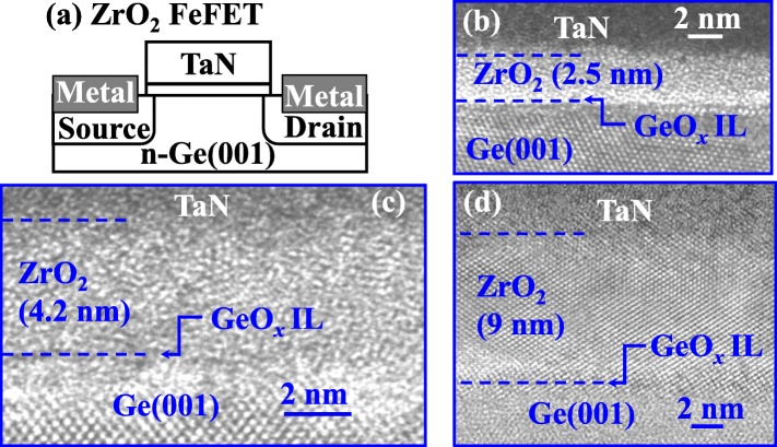
Figure 1 a shows the schematic of the fabricated transistor. Figure 1b–d shows the transmission electron microscope (TEM) images of the TaN/ZrO2/Ge samples with 2.5, 4, and 9 nm-thick ZrO2, respectively. All the samples underwent an RTA at 500 °C for 30 s. The 2.5 nm ZrO2 sample remains an insulator film after the annealing. For the 4 nm sample, although some nanocrystals are observed, ZrO2 maintains to be an amorphous layer. While full crystallization occurs for the 9 nm ZrO2 film. Notably, an interfacial layer (IL) of GeOx exists between the ZrO2 and Ge channel region, although it is too thin to be observed in the TEM images.
Fig. 1.
a Schematic of the fabricated TaN/ZrO2/Ge FeFET. b, c, and d HRTEM images of the TaN/ZrO2/Ge stacks with different ZrO2 thicknesses. The samples underwent an RTA at 500 °C for 30 s
Results and Discussion
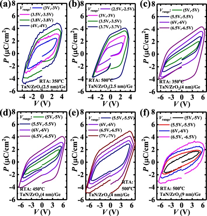
Figure 2 shows the P vs. voltage (V) curves for the TaN/ZrO2/Ge capacitors with different ZrO2 thicknesses and different annealing temperatures. The solid lines with different colors represent the minor loops with various sweeping voltage range (Vrange). The measurement frequency is 1 kHz. The 2.5 nm and 4 nm ZrO2 devices can exhibit stable ferroelectricity after an RTA at 350 °C. Figure 3 plots the remnant P (Pr) as a function of the sweeping V range curves for the capacitors annealed at various temperatures.
Fig. 2.
Measured P vs. V characteristics of the TaN/ZrO2/Ge capacitors with different ZrO2 thicknesses and various annealing temperatures
Fig. 3.
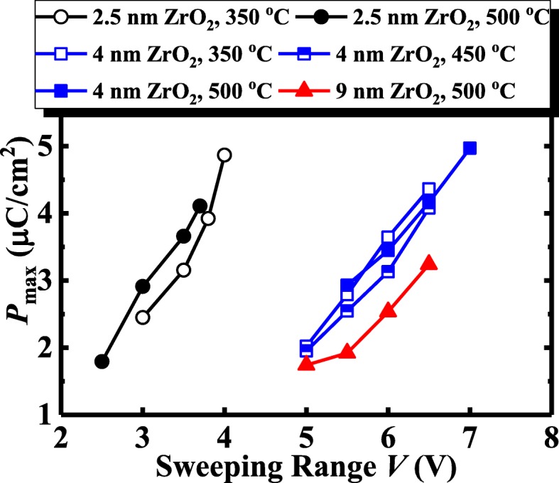
Comparison of Pmax as a function of Vrange for the TaN/ZrO2/Ge capacitors with different ZrO2 thicknesses and various annealing temperatures
Figure 3 shows the comparison of Pmax as a function of Vrange for the TaN/ZrO2/Ge capacitors with the different ZrO2 thicknesses and the various RTA temperatures. For the 4 nm ZrO2 devices, as the annealing temperature increases from 350 to 450 °C, a larger Vrange is required to obtain a fixed Pmax. This is attributed to the fact that the higher annealing temperature produces the thicker interfacial layers (ILs) between at Ge/ZrO2 and ZrO2/TaN interfaces, leading to a larger unified capacitance equivalent thickness (CET). For the 2.5 nm ZrO2 capacitors, the sample with 500 °C annealing has a lower Vrange than does the 350 °C annealing sample with the same Pmax. Although the ILs get thicker with the increased RTA temperature, some ZrO2 was consumed by the oxygen scavenging and interdiffusion at the interface. For the very thin ZrO2 device, the latter is dominant. Compared to the 2.5 nm ZrO2 capacitor, a much larger Vrange is required to achieve a similar Pmax. However, the 9 nm ZrO2 capacitor does not exhibit the higher Vrange in comparison with the 4 nm device. This is due to the crystal ZrO2 that has a much higher κ value than does the amorphous film, which significantly reduces the CET of the 9 nm device.
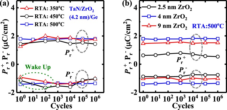
Figure 4a shows the extracted evolution of the positive and negative Pr, denoted by and , respectively, for the 4 nm-thick ZrO2 capacitors with RTA at different temperatures over 106 sweeping cycles measured at 1 kHz. Devices annealed at 350 °C and 450 °C exhibit the obvious wake-up effect. No wake up or imprint is observed for the 4 nm ZrO2 ferroelectric capacitor underwent annealing at 500 °C. Figure 4b compares the Pr as a function of sweeping cycles for the devices with the different ZrO2 thicknesses. The 4 nm ZrO2 ferroelectric capacitor achieves improved stability of Pr endurance compared to the 2.5 nm and 9 nm devices during the 106 endurance test.
Fig. 4.
aPr vs. the number of ms-pulse sweeping cycles for 4 nm ZrO2 capacitors with different RTA temperatures. bPr vs. number of ms-pulse sweeping cycles for the ZrO2 capacitors after annealing at 500 °C
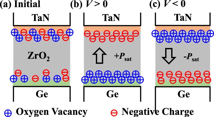
The switching P is observed in amorphous ZrO2 capacitance, and it is inferred that the mechanism must be different from that of the reported doped poly-HfO2 ferroelectric films. We propose that the underlying mechanism for ferroelectric behavior is related to the oxygen vacancy dipoles. It is well known that, as TaN metal deposited, the Ta oxygen scavenger layers will increase the oxygen vacancy concentration inside ZrO2 [10]. Oxygen vacancies also appear at the ZrO2/Ge interface. Figure 5 shows the schematics of the switchable P in TaN/ZrO2/Ge originating from the migration of oxygen vacancies and negative charges to form the positive and negative dipoles. It is speculated that the negative charges in ZrO2 are related to the Zr vacancy [11], which is similar to those in Al2O3 film [12]. The migration of the voltage-driven oxygen vacancies has been widely demonstrated in resistive random-access memory devices [13, 14]. Notably, this is the first demonstration of three-terminal non-volatile transistors dominated by the voltage-driven oxygen vacancies.
Fig. 5.
Schematics of the mechanism for switchable P in ZrO2 capacitors, which is attributed to the migration of voltage-driven oxygen vacancies and negative charges to form dipoles
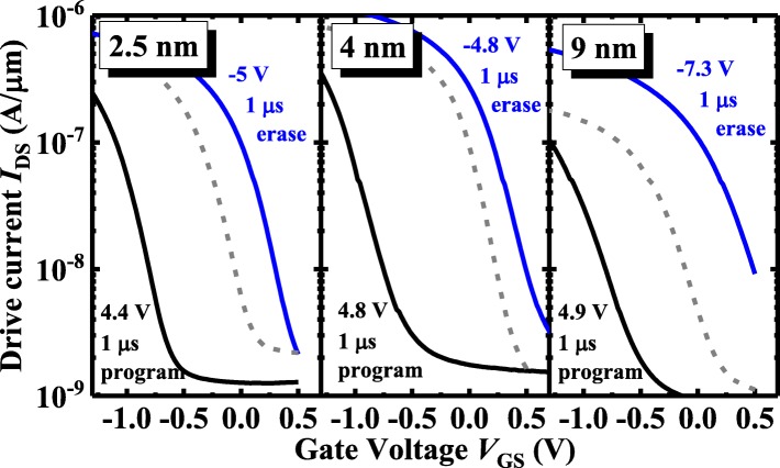
The P-V hysteresis enables the ZrO2 FeFETs to obtain a large and stable MW for the embedded NVM (eNVM) applications. Figure 6 shows the measured IDS-VGS curves of 2.5, 4, and 9 nm ZrO2 FeFETs for the two polarization states with 1 μs program/erase (P/E) conditions. The transistors were annealed at 500 °C. Program (erase) operation is achieved by applying positive (negative) voltage pulses to the gate of the ZrO2 FeFETs, to raise (lower) its threshold voltage (VTH). VTH is defined as VGS at 100 nA·W/L, and MW is defined as the maximum change in VTH. All the FeFETs with various ZrO2 thicknesses have the MW above 1 V with 1 μs P/E pulses. To achieve a similar MW, a higher erase voltage is needed for the 9 nm ZrO2 FeFET compared to the other two transistors. It is seen that a larger magnitude erase VGS is required to obtain the roughly equal shift of I-V relative to the initial curve compared to the program VGS. It is speculated that the oxygen vacancies contributing to the P mainly come from the reaction between TaN and ZrO2, like the initial state of the device in Fig. 5a. As a positive VGS (program) is applied, the oxygen vacancies diffuse and accumulate in the layer near the ZrO2/Ge interface (Fig. 5b), where the distribution of the oxygen vacancy dipoles is quite different from the initial state. So it is easy to shift the I-V curve to a higher |VTH| with a positive VGS. However, as a negative VGS (erase) is applied, the back diffusion of oxygen vacancies brings the gate stack back to its original state (Fig. 5c). So the magnitude of the negative erase VGS has to be increased to achieve the equivalent shift of I-V to the positive program VGS.
Fig. 6.
Measured IDS-VGS curves of the 2.5, 4, and 9 nm-thick ZrO2 FeFETs for the initial and two polarization states with 1 μs P/E pulses
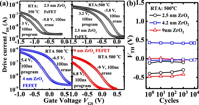
As the P/E pulse width is reduced to 100 ns, the ZrO2 FeFETs still demonstrate the decent MW, as shown in Fig. 7a. Especially, the transistor with 2.5 nm ZrO2 annealed at 350 °C achieves an MW of 0.28 V. Figure 7b plots MW vs. cycle number for the FeFETs with various ZrO2 thicknesses with 100 ns P/E pulse condition. The 4 nm ZrO2 device achieves a significantly improved endurance performance compared to the 2.5 nm and 9 nm ZrO2 FeFETs, which exhibit the obvious wake-up effect and fatigue within 103 cycles.
Fig. 7.
aIDS-VGS curves of the 2.5, 4, and 9 nm-thick ZrO2 FeFETs for the two polarization states with 100 ns P/E pulses. The devices underwent an RTA at 500 °C. b FeFET with 4 nm ZrO2 has an improved endurance compared to the 2.5 and 9 nm ZrO2 transistors
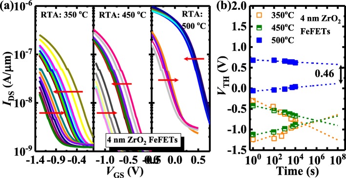
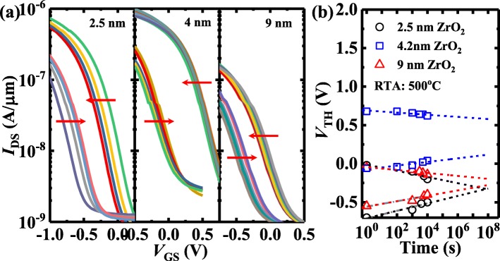
Finally, the retention testing of the ZrO2 FeFETs is characterized and shown in Figs. 8 and 9. Figure 8 a shows the evolution of IDS-VGS curves for the two polarization states of the 4 nm ZrO2 FeFETs underwent RTA at 350, 450, and 500 °C. The charge trapping leads to the reduction of the devices with the time. As shown in Fig. 8b, the retention performance of the devices can be improved with the increase of the RTA temperature. An MW of ~ 0.46 V is extrapolated to be maintained over 10 years. Figure 9 compares the retention characteristics of the FeFETs with different ZrO2 thicknesses. The 4 nm ZrO2 device has an improved retention performance compared to the transistors with 2.5 and 9 nm-thick ZrO2.
Fig. 8.
a The evolution of IDS-VGS curves for the two polarization states of the 4 nm ZrO2 FeFETs with different RTA temperatures. b The 4 nm ZrO2 device annealed at 500 °C has a much better retention performance compared to the transistors with RTA at the lower temperatures
Fig. 9.
a The evolution of IDS-VGS curves for the two polarization states for the 2.5, 4, and 9 nm-thick ZrO2 FeFETs underwent a RTA at 500 °C. b The 4 nm ZrO2 device has an improved retention performance compared to the transistors with 2.5 and 9 nm-thick ZrO2
Conclusions
In summary, amorphous ZrO2 ferroelectric capacitors are experimentally demonstrated, and the ferroelectricity is speculated to be due to the migration of the voltage-driven dipoles formed by the oxygen vacancies and negative charges. FeFETs with 2.5 nm, 4 nm, and 9 nm ZrO2 have the MW above 1 V with 1 μs P/E pulses. The improved fatigue and retention characteristics are obtained in the 4 nm-thick ZrO2 FeFET in comparison with the devices with 2.5 nm and 9 nm ZrO2. The retention test indicates that the 4 nm ZrO2 transistor keeps an extrapolated 10-year MW of ~ 0.46 V.
Acknowledgements
Not applicable.
Abbreviations
- RTA
Rapid thermal anneal
- IL
Interfacial layer
- TaN
Tantalum nitride
- FeFET
Ferroelectric field-effect transistors
- TDMAZr
Tetrakis (dimethylamido) zirconium
- Ge
Germanium
- ZrO2
Zirconium dioxide
- ALD
Atomic layer deposition
- HF
Hydrofluoric acid
- BF2+
Boron fluoride ion
- MW
Memory window
- NVM
Non-volatile memory
- Pr
Remnant polarization
- TEM
Transmission electron microscope
- Ni
Nickel
- Pmax
Maximum polarization
- RTA
Repaid thermal annealing
- Vrange
Sweeping voltage range
Authors’ Contributions
HL and YP carried out the experiments and drafted the manuscript. GQH and YL supported the study and helped to revise the manuscript. NZ and CGD helped to do the polarization measurement. YH provided constructive advice in the drafting. All the authors read and approved the final manuscript.
Funding
The authors acknowledge the support from the National Key Research and Development Project (Grant No. 2018YFB2202800 and 2018YFB2200500) and the National Natural Science Foundation of China (Grant No. 91964202, 61534004, and 61874081).
Availability of Data and Materials
The datasets supporting the conclusions of this article are included in the article.
Competing Interests
The authors declare that they have no competing interests.
Footnotes
Publisher’s Note
Springer Nature remains neutral with regard to jurisdictional claims in published maps and institutional affiliations.
Huan Liu and Yue Peng contributed equally to this work.
Contributor Information
Huan Liu, Email: xin_pzh@163.com.
Yue Peng, Email: 15029994289@163.com.
Genquan Han, Email: hangenquan@gmail.com, Email: gqhan@xidian.edu.cn.
Yan Liu, Email: xdliuyan@xidian.edu.cn.
Ni Zhong, Email: nzhong@ee.ecnu.edu.cn.
Chungang Duan, Email: cgduan@clpm.ecnu.edu.cn.
Yue Hao, Email: yhao@xidian.edu.cn.
References
- 1.Böscke T. S., Müller J., Bräuhaus D., Schröder U., Böttger U. Ferroelectricity in hafnium oxide thin films. Applied Physics Letters. 2011;99(10):102903. doi: 10.1063/1.3634052. [DOI] [Google Scholar]
- 2.Müller J, Böscke T.S, Muller S, Yurchuk E, Polakowski P, Paul J, Martin D, Schenk T, Khullar K, Kersch A, Weinreich W, Riedel S, Seidel K, Kumar A, Arruda T.M, Kalinin S.V, Schlösser T, Boschke R, Bentum R, Schröder U, Mikolajick T (2013) Ferroelectric hafnium oxide: a CMOS-compatible and highly scalable approach to future ferroelectric memories. In: IEDM Tech. Dig. pp 10.8.1-10.8.4
- 3.Varghese Justin, Barth Sven, Keeney Lynette, Whatmore Roger W., Holmes Justin D. Nanoscale Ferroelectric and Piezoelectric Properties of Sb2S3 Nanowire Arrays. Nano Letters. 2012;12(2):868–872. doi: 10.1021/nl2039106. [DOI] [PubMed] [Google Scholar]
- 4.Mukherjee S, Roy A, Auluck S, Prasad R, Gupta R, Garg A. Room temperature nanoscale ferroelectricity in magnetoelectric epitaxial thin films. Phys. Rev. Lett. 2013;111:087601. doi: 10.1103/PhysRevLett.111.087601. [DOI] [PubMed] [Google Scholar]
- 5.Bark C. W., Sharma P., Wang Y., Baek S. H., Lee S., Ryu S., Folkman C. M., Paudel T. R., Kumar A., Kalinin S. V., Sokolov A., Tsymbal E. Y., Rzchowski M. S., Gruverman A., Eom C. B. Switchable Induced Polarization in LaAlO3/SrTiO3 Heterostructures. Nano Letters. 2012;12(4):1765–1771. doi: 10.1021/nl3001088. [DOI] [PubMed] [Google Scholar]
- 6.Peng Y, Xiao WW, Han GQ, Liu Y, Wu JB, Wang K, He ZH, Yu ZH, Wang XR, Xu N, Liu TJK, Hao Y. Nanocrystal-embedded-insulator (NEI) ferroelectric field-effect transistor featuring low operating voltages and improved synaptic behavior. IEEE Electron Device Letters. 2019;40:1933–1936. doi: 10.1109/LED.2019.2947086. [DOI] [Google Scholar]
- 7.Peng Y, Xiao WW, Han GQ, Wu JB, Liu H, Liu Y, Xu N, Liu TJK, Hao Y. Nanocrystal-embedded-insulator ferroelectric negative capacitance FETs with Sub-kT/q swing. IEEE Electron Device Letters. 2019;40:9–12. doi: 10.1109/LED.2019.2947086. [DOI] [Google Scholar]
- 8.Liu Huan, Wang Chengxu, Han Genquan, Li Jing, Peng Yue, Liu Yan, Wang Xingsheng, Zhong Ni, Duan Chungang, Wang Xinran, Xu Nuo, Liu Tsu-Jae King, Hao Yue. ZrO2 Ferroelectric FET for Non-volatile Memory Application. IEEE Electron Device Letters. 2019;40(9):1419–1422. doi: 10.1109/LED.2019.2930458. [DOI] [Google Scholar]
- 9.Liu H, Zheng SY, Han GQ, Xu Y, Liu Y, Wang CX, Wang XS, Yang N, Zhong N, Hao Y (2019) ZrO2 Anti-ferroelectric field effect transistor for non-volatile memory and analog synapse applications. In: Proc. Ext. Abst. SSDM, pp. 379-380
- 10.Zhong X, Rungger I, Zapol P, Nakamura H, Asai Y, Heinonen O. The effect of a Ta oxygen scavenger layer on HfO2-based resistive switching behavior: thermodynamic stability, electronic structure, and low-bias transport. Physical Chemistry Chemical Physics. 2016;18(10):7502–7510. doi: 10.1039/C6CP00450D. [DOI] [PubMed] [Google Scholar]
- 11.Houssa M, Afanas’ev VV, Stesmans A, Heyns MM. Variation in the fixed charge density of SiOx/ZrO2 gate dielectric stacks during postdeposition oxidation. Appl Phys Letters. 2000;77(12):1885–1887. doi: 10.1063/1.1310635. [DOI] [Google Scholar]
- 12.Kojima E, Chokawa K, Shirakawa H, Araidai M, Hosoi T, Watanabe H, Shiraishi K. Effect of incorporation of nitrogen atoms in Al2O3 gate dielectric of wide-bandgap-semiconductor MOSFET on gate leakage current and negative fixed charge. Appl Phys Expr. 2018;11(6):061501. doi: 10.7567/APEX.11.061501. [DOI] [Google Scholar]
- 13.Bersuker G, Gilmer D.C, Veksler D, Yum J, Park H, Lian S, Vandelli L, Padovani A, Larcher L, Mckenna K, Shluger A, Iglesias V, Porti M, Nafría M, Taylor W, Kirsch P.D, Jammy R (2010) Metal oxide RRAM switching mechanism based on conductive filament microscopic properties. In: IEDM Tech Dig, pp 19-6
- 14.Xu N, Gao B, Liu, L.F, Sun B, Liu X.Y, Han R.Q, Kang J.F, Yu B (2008) A unified physical model of switching behavior in oxide-based RRAM. In: VLSI Tech Dig, pp 100-101
Associated Data
This section collects any data citations, data availability statements, or supplementary materials included in this article.
Data Availability Statement
The datasets supporting the conclusions of this article are included in the article.


