Abstract
Developing van der Waals (vdW) homojunction devices requires materials with narrow bandgaps and simultaneously high hole and electron mobilities for bipolar transport, as well as methods to image and study spatial variations in carrier type and associated conductivity with nanometer spatial resolution. Here we demonstrate the general capability of near-field scanning microwave microscopy (SMM) to image and study the local carrier type and associated conductivity in operando by studying ambiploar field effect transistors (FETs) of the 1D vdW material tellurium in 2D form. To quantitatively understand electronic variations across the device, we produce nanometer resolved maps of the local carrier equivalence backgate voltage. We show that the global device conductivity minimum determined from transport measurements does not arise from uniform carrier neutrality, but rather from the continued coexistence of p-type regions at the device edge and n-type regions in the interior of our micron-scale devices. This work both underscores and addresses the need to image and understand spatial variations in the electronic properties of nanoscale devices.
Keywords: Atomic Force Microscope, Microwave, Near-Field Microscopy, Field-Effect Transistor, 2D Materials
Graphical Abstract
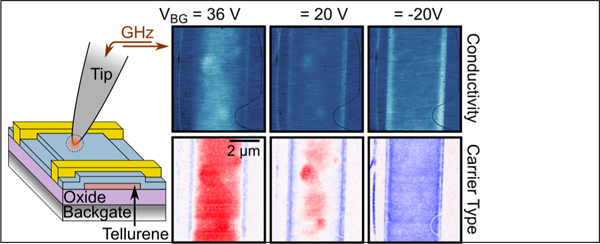
Developing fundamental circuit building blocks such as diodes and transistors 1 based on low-dimensional van der Waals (vdW) materials requires producing and controlling adjoining regions of p-type and n-type transport.2–7 While the broad library or vdW materials offers a range of novel functionalities such as memristors, 8 topologically protected states,9–11 or those based on magnetic12 and other spin-based phenomena, 13 MoS2 and the associated family of transition metal dichalcogenides (TMDs) remain the primary candidates for semiconducting applications. In these materials bipolar transport for homojunction devices can be difficult to achieve,2,14 and difficult-to-fabricate heterostructures remain the primary practical path for pn junctions and other basic semiconducting circuit elements. 7 A key challenge therefore remains the development and discovery of new materials for homojunction devices with the narrow bandgaps and simultaneously high hole and electron mobilities15–17 desired for bipolar transport.
Nanometer thin films of elemental tellurium have recently been demonstrated for device applications.17 Tellurium is a vdW material whose helical 1D atomic chains can be assembled into 1D filaments18 or 2D films (tellurene)17,19 and deposited using solution-based processes. Tellurene in particular exhibits both n- and p-type mobilities as high as 700 cm2/V·s, and the thickness-dependent bandgap as small as 0.4 eV17 readily enables bipolar transport. 20 Unlike black phosphorous, another promising material exhibiting bipolar transport, 15,16 tellurene is stable under ambient conditions and resistant to long-term deterioration. Dopant incorporation is often difficult in 2D vdW materials, and the solution-based synthesis of tellurene further offers an attractive avenue for doping, but successful exploitation of this feature requires a detailed understanding of the resulting local transport properties and their relation to growth conditions. It is thus of critical importance to be able to address and study not only the local carrier density and associated conductivity in functional devices with nanometer spatial resolution, but to be able to do so in a manner that is also sensitive to the carrier type.
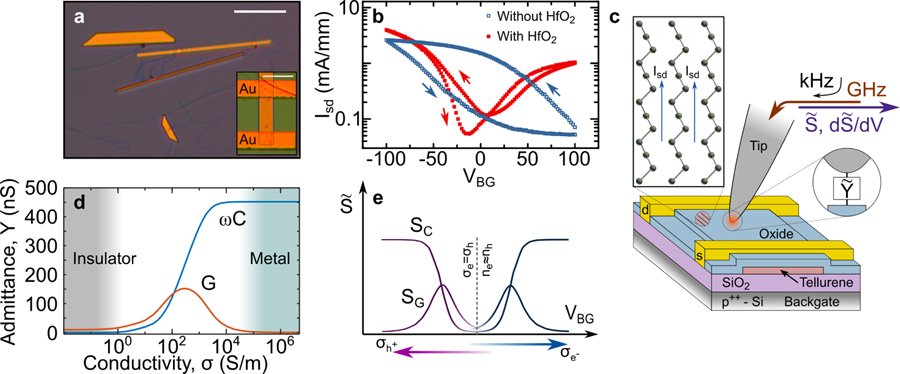
An optical micrograph of representative trapezoidal tellurene flakes deposited on SiO2 is shown in Fig. 1a). Also seen in the optical micrograph are the curved string-like 1D Te filaments that result as a by-product from solution growth. 18 After contact electrodes are fabricated via electron beam lithography, devices are encapsulated in 10 nm of conformal oxide using atomic layer deposition (ALD) of either HfO2 or Al2O3. Shown in Fig. 1b) is the backgate voltage (VBG)-dependent transport characteristic of a tellurene FET before and after ALD deposition, acquired with a source-drain bias of Vsd = 0.05 V. In addition to preventing device failure due to tip-sample conduction, the ALD encapsulation also reduces device hysteresis and enables bipolar transport,20 likely due to oxygen vacancy-induced n-doping.21
Figure 1:
(a) Optical micrograph of solution-grown tellurene crystals showing characteristic trapezoidal shape as well as string-like Te filaments formed during process (scale bar: 20 µm). Inset: Optical micrograph of a tellurene device (scale bar: 8 µm). (b) Transport characteristics of a tellurene FET before and after deposition of a 10 nm conformal HfO2 overcoat. (c) Schematic of the experimental setup illustrating the transport along the direction of the atomic Te chains. (d) Finite element modeling of the complex-valued tip-sample admittance at 17.3 GHz as a function of tellurene conductivity. (e) Illustration of the expected measured microwave signal as a function of VBG for an ambipolar FET showing clear regimes of contrast corresponding to hole- and electron-conductivity.
An illustration of the experimental setup is shown in Fig. 1c) with the scanning microwave microscope (SMM, also called scanning microwave impedance microscopy, sMIM) based on an atomic force microscope (AFM) operating in contact mode that detects the phase-resolved real and imaginary components of the microwave signal . The simulated (COMSOL 4.2*) tip-sample admittance for a unipolar tellurene device is shown in Fig. 1d) with the conductance G and capacitance C as a function of the tellurene conductivity σi = nieµi with the elementary charge e, carrier density ni, and corresponding carrier mobility µi (i = h, e). Assuming (i.e., SG ∝ G and SC ∝ C),22–24 the SMM sensitivity peaks at σ = 300 S/m yet remains sensitive over the range σ ≈ 100 – 104 S/m. Controlling the carrier type and concentration using the global backgate VBG, we expect the measured signal to evolve as schematically illustrated in Fig. 1e) with two distinct regions of sensitivity as the device transitions between the hole and electron transport regimes.
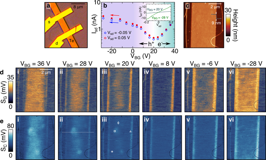
Shown in Fig. 2a) is an optical micrograph of a tellurene FET fabricated on 90 nm SiO2, with source and drain electrodes as indicated and a channel length of 8 µm. Shown in Fig. 2b) is the source-drain current Isd measured at Vsd = ±0.05 V, showing a clear global conductivity minimum (carrier equivalence) point at VBG = 20 V separating the hole and electron transport regimes as indicated.
Figure 2:
(a) Optical micrograph of an Al2O3-encapsulated tellurene device with source and drain electrodes as indicated. (b) Transport characteristics of the device, with the global device carrier equivalence point at VBG = 20 V and electron and hole transport regimes as indicated. Inset: The IV characteristics of the device at VBG as indicated with near-ohmic behavior, though some nonlinearity and increased noise are seen at positive Vsd. (c) Contact mode AFM topography of the device active area (source and drain electrodes are just out of view at image top and bottom). (d) and (e) show SMM images acquired at sequentially decreasing values of VBG as indicated, with the conductance SG and capacitive SC channels, respectively.
The contact-mode AFM topography in Fig. 2c) shows a uniform device with a thickness of ∼9 nm and only small topographic variations. Also visible are co-deposited Te filaments, including one over the device. A sequence of SG and SC images at select voltages are shown in Fig. 2d) and e), respectively (see supporting information for full data set). For large and positive VBG the device is in the electron-transport regime, and the higher signals in both channels indicate that the device interior is more conductive than the device edges. As VBG decreases and approaches the global device carrier equivalence point at VBG = 20 V, the interior of the device becomes less conductive while the edge conductivity increases. When VBG is further decreased and the device transitions into the hole-conduction regime, we see the conductivity in the device interior reach a minimum at VBG = 8 V while the edge conductivity continues to increase monotonically. As VBG is decreased beyond the conductivity minimum of the device interior, the conductivity in this region is seen to increase again, though over the voltage range accessible with this device it does not reach parity with the edges again. Observed differences between SG and SC in high-conductivity regions are expected, as the former does not increase monotonically with conductivity.
Several notable features stand out from the sequence of microwave near-field images. In particular, the device interior does show spatial conductivity variations. The filament also affects the measured signal, although this appears to be limited to reducing the overall signal due to the increased tip-sample spacing, and no electronic effects arise in its vicinity. Most importantly, the discrepancy in VBG-dependent behavior between the device interior and exterior suggests inhomogeneities in the carrier type and we perform additional measurements to better understand this behavior.
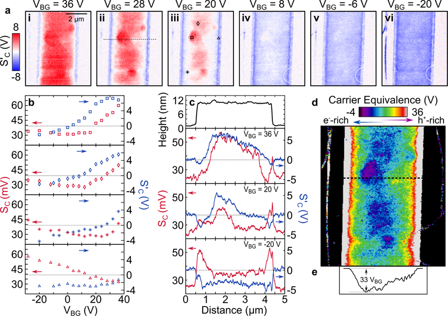
Differential measurements are sensitive to the slope of the conductivity-dependent signal. Shown in Fig. 3a) are the 22,25 images corresponding to the SC images shown in Fig. 2d) and e) (see supporting information for full data set, including ). The sign of directly reflects the carrier type locally present beneath the tip, and gives a direct measure of the local p- or n-type character of the tellurene device. For instance, over a p-type region the positive part of the Vtip modulation cycle locally depletes (repels) p-type carriers and thus reduces the conductivity, giving an out-of-phase response (, blue regions). For the n-type regions the opposite will occur, where the positive portion of the cycle accumulates (attracts) n-type carriers and thus increases conductivity, yielding an in-phase response (, red regions).
Figure 3:
(a) images acquired at VBG as indicated. (b) and SC as a function of VBG acquired at the locations of the corresponding symbols in a)iii) and Fig. 2e)iii). (c) Line cuts across the tellurene device showing the topography (top) and and SC at values of VBG as indicated, taken from the location of the dashed line in a)ii) and Fig. 2e)ii). Dashed lines in b) and c) are a guide to the eye at . (d) Spatially resolved map of the local carrier equivalence voltage. (e) Line cut taken along the dashed line in d) showing a variation of VBG > 33 V across the device.
Together with SC, provides a more comprehensive understanding of these devices. Shown in Fig. 3b) are the VBG-dependent SC and signals at the position of the corresponding symbols in Fig. 2e)iii) and Fig. 3a)iii). For the three positions within the device interior, SC decreases with decreasing VBG, reaches a minimum value at the local carrier equivalence point, and then increases again, while crosses zero (dashed lines) at the same VBG values as the minima of SC, confirming their differential relationship. At the device edge, SC increases monotonically with decreasing VBG while remains negative over the full voltage range as expected.
We next take a closer look at the spatial variations in and SC across the tellurene device. Shown in Fig. 3c) are line cuts taken at the position of the dashed line in Fig. 2e)ii) and Fig. 3c)ii) with the topography (top panel) and corresponding and SC cuts at values of VBG as indicated. At large positive bias the conductivity is highest in the interior of the crystal where the positive reflects the n-type behavior measured by transport while the edges appear weakly conductive with the negative signal, revealing p-type conductivity well above the global carrier equivalence point. At the global device carrier equivalence point we see a clear coexistence between p-type behavior at the edges and spatially inhomogeneous n-type behavior within the device interior. Comparison with SC reveals that the p-type edges are significantly more conductive than most of the device interior at this point, though over a significantly smaller area. Once the device has transitioned to uniform p-type behavior at VBG = −20 V, the conductivity profile is inverted with higher conductivity near the edges, though clear inhomogeneities remain.
The device edge can experience enhanced local electric fields due to fringing and resulting concentration of the fields from the backgate. However, the strong p-type character at the edges cannot be explained by field fringing, where the enhancement of the electric field from the global backgate at the crystal edges would reduce the hole density at positive backgate biases relative to the device interior, contrary to observations. Similarly, modification and enhancement of the tip-sample fields are possible with the tip positioned at the edge of the crystal. Our estimated spatial resolution of <60 nm (see supporting information) provides the lateral distance over which the tip-edge interaction is expected to decay as the tip moves toward the device interior. The edge conductivity variations persist for several 100 nm from the edge and thus originate from material properties rather than effects of local field concentration at the device edges.
In order to fully understand the variations in carrier type we construct a nanometer-resolved carrier equivalence voltage map. To take advantage of the improved contrast of lock-in detection and to avoid uncertainty in the location of the SC minima, we interpolate the VBG-dependent zero crossing of to determine the local carrier equivalence point. Shown in Fig. 3d) is a spatially resolved map of the local carrier equivalence voltage at each spatial pixel in as determined from the full sequence of images (see supporting information).26 This carrier equivalence map reveals the complex variations in carrier type and density across the device. Note that white regions at the device edges have a carrier equivalence point greater than 36 VBG. The line cut along the dashed line in Fig. 3d), shown in Fig. 3e), underscores the degree of spatial inhomogeneity across the device with lateral variation in the local equivalence point of VBG > 33 V.
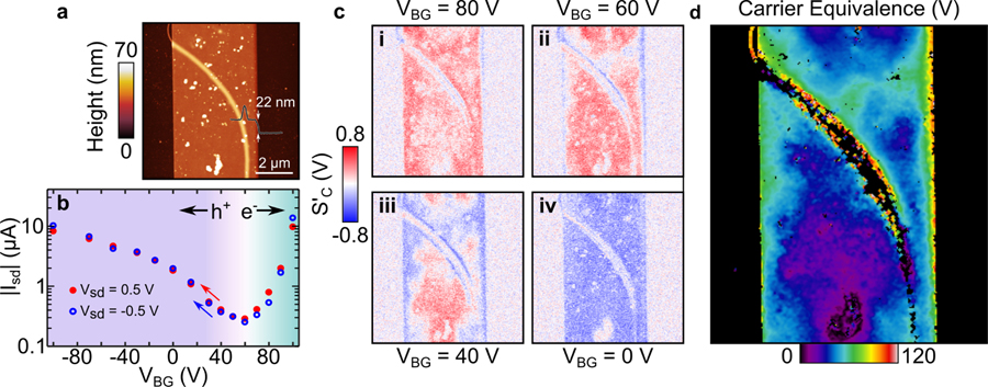
While thin devices are largely uniform along the transport axis (see supporting information for an additional device), large variations in behavior are seen for other devices. Shown in Fig. 4a) is the AFM topography of a device where a tellurene filament is embedded beneath the crystal. This device, encapsulated with HfO2, is deposited on 300 nm of SiO2, which results in a lower backgate efficiency that requires larger voltages up to VBG = ±100 V, and has a global carrier equivalence point of VBG = 60 V as shown in Fig. 4b). The sequence in Fig. 4c) shows the evolution of the conductivity from n-type to p-type, with higher hole density at the device edges and an overall electron-rich interior. However, the embedded filament induces a large degree of spatial inhomogeneity within the crystal, as underscored by the carrier equivalence map shown in Fig. 4d).
Figure 4:
(a) AFM topography of a tellurene device with embedded Te filament. (b) Transport characteristics of the device with a global carrier equivalence point of VBG = 60 V. (c) Sequence of images that illustrates the high degree of spatial inhomogeneity in carrier type and density present in this device as further seen in (d), the extracted carrier equivalence map.
The origin of the spatial variations in conductivity seen across these devices, most notably the significant differences between the edges and interior, is likely associated with several factors. One of the defining features of vdW materials is the capability of the weak interlayer interactions to accommodate the intercalation of dopants,27,28 and growth kinetics may favor incorporation of different types or concentrations of p-dopants later in the growth process when the edge termination is formed. We also observe that all images, including the carrier equivalence maps, show local spatial variations in electronic behavior on 10s of nanometer length scales. While these weakly correlate with structure in the topography (see supporting information), the possible influence of vdW assembly, including molecular alignment and possibly interfacial effects, is hard to discern due to the indistinguishability of underlying crystal features from thickness variations in the ALD overcoat. We note the prevalent strong p-type character and associated high local carrier equivalence voltage within the device interior near the embedded Te filament. This region immediately adjacent to the filament likely experiences significant tensile strain that appears to produce similar electrical characteristics to the edges. This suggests that strain strongly influences the carrier density and type. As the filaments appear to have p-type character, it is also possible that the filament induces local p-doping, although the region immediately on top of the embedded filament as well as the vicinity of filaments on top of devices do not appear p-type. Lastly, although n-type doping due to the ALD overcoat20,21 would be expected to be stronger at the edges where the surface-to-volume ratio is higher, we cannot rule out interfacial impurities and associated fermi-level pinning as contributing factors.
The capability to study and image local variations in conductivity with nanometer spatial resolution has been a long-standing challenge for scanning probe methods. Optical near-field methods can be used to study conductivity variations in highly doped materials, 29 and while related near-field photocurrent microscopy has shown potential for graphene30 its general application has not been explored. In particular, the differential implementations of SMM and closely related scanning capacitance microscopy (SCM) have previously been used to study the local carrier type in model systems. 22,25,31 On the other hand, conventional SMM can be used to study nanoscale devices24,32 but has not yet been applied to ambipolar devices.
Studying devices in operando requires non-destructive probing in a compatible geometry, and AFM-based methods such as kelvin probe force microscopy33,34 or conductive-AFM35 are well suited for such measurements. However, device encapsulation to prevent destructive electrical discharge from the tip precludes the use of these methods. This work is thus enabled by leveraging the subsurface imaging capability of SMM 24,36 and combining for the first time the conductivity sensing capability of the signal and the carrier-specific imaging of to study bipolar transport in active devices.
Here we have shown how the unique capabilities of microwave near-field microscopy can be used to study the spatial variations in electronic properties of ambiploar field effect transistors. In addition to the established capability to image and study spatial variations in sample conductivity, we use differential imaging to determine the local carrier type throughout the backgate voltage-controlled evolution of the device transport properties. We find large variations in our tellurene devices, with strong p-type conductivity observed at the edge of all devices and lower p-type conductivity in the device interior that can readily be switched to n-type behavior at positive backgate biases. Our measurements reveal that global transport measurements belie the nanoscale complexity of the device, where we show that the device-average carrier equivalence point is actually the result of the simultaneous coexistence of p-type and n-type regions that give rise to an overall minimum conductivity rather than true carrier neutrality. We identify significant variations in the local carrier equivalence point across active devices due to structural variations, interfacial effects, as well as the influence of local strain. These results underscore the importance of understanding local variations in carrier density and type, and provide a direct means to evaluate the intercalation of dopants into vdW materials. Our approach can be broadly used to understand and guide the development of low-dimensional semiconducting device architectures and functionalities based on bipolar transport that can be controlled or switched by applied strain or other stressors.
Methods.
Tellurene devices studied here are fabricated as described previously. 17 Tellurene films are grown by a solution-based process and deposited using a Langmuir-Blodgett process onto p++-Si substrates covered by thermally deposited silicon dioxide, and contact electrodes are fabricated via electron beam lithography. Devices are subsequently encapsulated in 10 nm of conformal oxide (HfO2 or Al2O3) using atomic layer deposition. The devices are then mounted to the AFM scanner and the leads wirebonded to enable electrical measurements and backgate voltage control in situ.
The SMM is based on a modified commercial AFM/SMM system (Keysight*) operating in contact mode.22 The microwave signal at ∼17.3 GHz is sourced from a vector network analyzer and delivered via the tip to the sample using a coaxial resonator, and the reflected signal is detected using an IQ mixer (Analog Devices*). A phase controlled reference signal is used to separate the real and imaginary components . Differential measurements are performed by applying an AC tip bias Vtip at a frequency of 50 kHz and an amplitude of Vp−p = 1 V. Lock in detection of the analog output of the IQ mixer yields the differential signals and .22,25
We note that the differential relationship between and suggests that a single measurement would be sufficient and the other data channel can be determined via numerical integration or differentiation at each spatial pixel. However, differential operations performed on a sequence of scans significantly increase the noise and are highly susceptible to sample drift. In principle, if sufficient stability is achieved the higher contrast in could enable integration, though large backgate voltages beyond device breakdown would nevertheless be required to establish the constant of integration.
While these devices are hysteretic, we find that systematic VBG-dependent measurement sequences can yield a high degree of reproducibility. In particular, we achieve this by sequentially acquiring single SMM images at each decreasing value of VBG followed by a current-voltage (IV) sweep. We note that the device global conductivity minimum extracted from the sequence of IV curves corresponds to the condition where σe = σh. However, measurements of both field effect20 and low-temperature Hall mobilities19 suggest that µe ≈ µh along the atomic chains, and theoretical work37 suggests comparable effective masses and thus mobilities for electrons and holes across the atomic chains as well. While the microwave near-field probes transport both across and along the atomic chains, the conductivity minimum thus also corresponds approximately to the carrier equivalence (charge neutrality) point.
The conductivity-dependent microwave signal was simulated using COMSOL 4.2 in an approach previously validated for nanoscale systems in general23 and 2D materials in particular.22,24,36 The AC/DC package was used at a frequency of 17.3 GHz with an axisymmetric geometry with a semi-infinite sample to minimize computation times. The geometry consisted of a metallic parabolic tip with a radius of 20 nm in contact with a 10 nm film of Al2O3 (ϵ = 10) covering a 9 nm thick sample of varying conductivity (Te crystal) that is separated from the conductive Si backgate (σ = 104 S/m) by 90 nm SiO2 (ϵ = 3.9).
Supplementary Material
Acknowledgments
We would like to thank Kevin J. Coakley for valuable discussions. The work at Purdue University is partly supported by NSF grant no. CMMI-1663214 and the Army Research Office under grant nos. W911NF-15-1-0574 and W911NF-17-1-0573
Footnotes
Mention of commercial products is for informational purposes only, it does not imply NIST’s recommendation or endorsement. Contributions of the National Institute of Standards and Technology, not subject to copyright in the United States.
Supporting Information
We provide the full data sets for all scans, data for an additional homogeneous device, and a high-resolution scan of a device. This material is available free of charge via the Internet at http://pubs.acs.org.
References
- (1).Sze S; Ng K Semiconductor Devices; John Wiley & Sons, 2007. [Google Scholar]
- (2).Ross DS; Klement P; Jones AM; Ghimire NJ; Yan J; Mandrus DG; Taniguchi T; Watanabe K; Yao W; Cobden DH; Xu X Nat. Nanotech 2014, 9, 268. [DOI] [PubMed] [Google Scholar]
- (3).Pospischil A; Furchi MM; Mueller T Nat. Nanotechnol 2014, 9, 257. [DOI] [PubMed] [Google Scholar]
- (4).Baugher BWH; Churchill HOH; Yang Y; Jarillo-Herrero P Nat. Nanotechnol 2014, 9, 262. [DOI] [PubMed] [Google Scholar]
- (5).Buscema M; Groenendijk DJ; Steele GA; van der Zant HSJ; Castellanos-Gomez A Nat. Comms 2014, 5, 4651. [DOI] [PubMed] [Google Scholar]
- (6).Duan X; Wang C; Shaw JC; Cheng R; Chen Y; Li H; Wu X; Tang Y; Zhanbg Q; Pan A; Jiang J; Yu R; Huang Y; Duan X Nat. Mater 2014, 9, 1024. [DOI] [PubMed] [Google Scholar]
- (7).Liu Y; Weiss NO; Duan X; Cheng HC; Huang Y; Duan X Nat. Rev. Mater 2016, 1, 16042. [Google Scholar]
- (8).Sangwan VK; Lee HS; Bergeron H; Balla I; Beck ME; Chen KS; Hersam MC Nature 2018, 554, 500. [DOI] [PubMed] [Google Scholar]
- (9).Kou L; Wu a S. C.,; Felser C; Frauenheim T; Chen C; Yan B ACS Nano 2014, 8, 10448. [DOI] [PubMed] [Google Scholar]
- (10).Ju L; Shi Z; Nair N; Lv Y; Jin C; Velasco J Jr.; Ojeda-Aristizabal C; Bechtel HA; Martin MC; Zettl A; Analytis K; Wang F Nature 2015, 520, 650. [DOI] [PubMed] [Google Scholar]
- (11).Zhang H; Liu CX; Qi XL; Dai X; Fang Z; Zhang SC Nat. Phys 2009, 5, 438. [Google Scholar]
- (12).Huang B; Clark G; Klein DR; MacNeill D; Navarro-Moratalla E; Seyler KL; Wilson N; McGuire MA; Cobden DH; Xiao D; Yao W; Jarillo-Herrero P; Xu X Nat. Nanotechnol 2018, 13, 544. [DOI] [PubMed] [Google Scholar]
- (13).Mak KF; McGill KL; Park J; McEuen PL Science 2014, 344, 1489. [DOI] [PubMed] [Google Scholar]
- (14).Chen JW; Lo ST; Ho SC; Wong SS; Vu THY; Zhang XQ; Liu YD; Chiou YY; Chen YX; Yang YC; et al. Nature Comms 2018, 9, 3143. [DOI] [PMC free article] [PubMed] [Google Scholar]
- (15).Das S; Demarteau M; Roelofs A ACS Nano 2014, 8, 11730. [DOI] [PubMed] [Google Scholar]
- (16).Liu H; Neal AT; Zhu Z; Luo Z; Xu X; Tománek T; Ye PD ACS Nano 2014, 8, 4033. [DOI] [PubMed] [Google Scholar]
- (17).Wang Y; Qiu G; Wang R; Huang S; Wang Q; Liu Y; Du Y; Goddard WA III; Kim MJ; Xu X; Ye PD; Wu W Nat. Electron 2018, 1, 228. [Google Scholar]
- (18).Mayers B; Xia Y J. Mater. Chem 2002, 12, 1875. [Google Scholar]
- (19).Du Y; Qiu G; Wang Y; Si M; Xu X; Wu W; Ye PD Nano Lett 2017, 17, 3965. [DOI] [PubMed] [Google Scholar]
- (20).Qiu G; Si M; Wang Y; Lyu X; Wu W; Ye PD High-performance few-layer tellurium CMOS devices enabled by atomic layer deposited dielectric doping technique. 2018 76th Device Research Conference (DRC). 2018; pp 1–2. [Google Scholar]
- (21).Valsaraj A; Chang J; Rai A; Register LF; Banerjee SK 2D Mater 2015, 2, 045009. [Google Scholar]
- (22).Berweger S; Weber JC; John J; Velazquez JM; Pieterick A; Sanford NA; Davydov AV; Brunschwig B; Lewis NS; Wallis TM; Kabos P Nano Lett 2015, 15, 1122. [DOI] [PubMed] [Google Scholar]
- (23).Lai K; Peng H; Kundhikanjana W; Schoen DT; Xie C; Meister S; Ciu Y; Kelly MA; Shen ZX Nano Lett 2009, 9, 1265. [DOI] [PubMed] [Google Scholar]
- (24).Wu D; Li X; Wu X; Li W; Yogeesh MN; Ghosh R; Chu Z; Akinwande D; Niu Q; Lai K Proc. Natl. Acad. Sci 2016, 113, 8583. [DOI] [PMC free article] [PubMed] [Google Scholar]
- (25).Huber HP; Humer I; Hochleitner M; Fenner M; Moertelmaier M; Rankl C; Imtiaz A; Wallis TM; Tanbakuchi H; Hinterdorfer P; Kabos P; Smoliner J; Kopanski JJ; Kienberger F J. Appl. Phys 2012, 111, 014301. [Google Scholar]
- (26).Pollard B; Muller EA; Hinrichs K; Raschke MB Nat. Comms 2014, 5, 3587. [DOI] [PMC free article] [PubMed] [Google Scholar]
- (27).Bediako DK; Rezaee M; Yoo H; Larson DT; Zhao SYF; Taniguchi T; Watanabe K; Brower-Thomas TL; Kaxiras E; Kim P Nature 2018, 558, 425. [DOI] [PubMed] [Google Scholar]
- (28).Xiong F; Wang H; Liu X; Sun J; Brongersma M; Pop E; Cui Y Nano Lett 2015, 15, 6777. [DOI] [PubMed] [Google Scholar]
- (29).Ritchie E; Hill DJ; Mastin TM; Deguzman PD; Cahoon JF; Atkin JM Nano Lett 2017, 17, 6591. [DOI] [PubMed] [Google Scholar]
- (30).Woessner A; Alonso-González P; Lundeberg MB; Gao Y; Barrios-Vargas JE; Navickaite G; Ma Q; Janner D; Watanabe K; Cummings AW; et al. Nat. Comms 2016, 7, 10783. [DOI] [PMC free article] [PubMed] [Google Scholar]
- (31).Edwards H; Ukraintsev VA; San Martin R; Johnson FS; Menz P; Walsh S; Ashburn S; Wills KS; Harvey K; Chang MC J. Appl. Phys 2000, 87, 1485. [Google Scholar]
- (32).Berweger S; Blanchard PT; Brubaker MD; Coakley KJ; Sanford NA; Wallis TM; Bertness KA; Kabos P Appl. Phys. Lett 2016, 108, 073101. [DOI] [PMC free article] [PubMed] [Google Scholar]
- (33).Wagner T; Beyer H; Reissner P; Mensch P; Riel H; Gotsmann B; Stemmer A Beilstein J. Nanotech 2015, 6, 2193. [DOI] [PMC free article] [PubMed] [Google Scholar]
- (34).Koren E; Berkovitch N; Azriel O; Boag A; Rosenwaks Y; Hemesath ER; ; Lauhon L J. Appl. Phys. Lett 2011, 99, 223511. [Google Scholar]
- (35).MacDonald GA; Yang M; Berweger S; Kabos P; Berry JJ; Zhu K; Del-Rio FW Energ. Environ. Sci 2016, 9, 3642. [Google Scholar]
- (36).Gramse G; Kölker A; Lim T; Stock TJZ; Solanki H; Schofield SR; Brincotti E; Aeppli G; Kienberger F; Curson NJ Sci. Adv 2017, 3, e1602586. [DOI] [PMC free article] [PubMed] [Google Scholar]
- (37).Liu Y; Wu W; Goddard W III J. Am. Chem. Soc 2018, 140, 550. [DOI] [PubMed] [Google Scholar]
Associated Data
This section collects any data citations, data availability statements, or supplementary materials included in this article.


