

Abstract
The performance of differential up-conversion passive mixer operating in the 3–5 GHz band for UWB transmitter driven by 25% duty-cycle clocks is studied and analyzed. A reasonably accurate LTI equivalent circuit accounting for harmonics is derived. We have demonstrated that the conversion gain, input and output impedances of the proposed LTI equivalent circuit matches those of the LTV up-conversion passive mixer. The LTI model can be used to define the reachable design space. The mixer input and output impedance can be tuned by varying resistor at the mixer output allowing for impedance match to connected circuits. We have shown how each design parameters impacts critical performance of the up-conversion passive mixer. Simulations of the proposed up-conversion passive mixer show −3.68 dB of conversion gain, 15.9 dBm of OIP3, 116.7dBm of OIP2 and a NF as low as 5.2 dB while consuming 1.5 pW. Furthermore linearity and ports isolation performances due to voltage threshold mismatch variation of ±60 mV shows an OIP3 greater than 15.85dBm and an LO_RF isolation smaller than −51.9 dB.
Keywords: UWB transmitter, Up-conversion passive mixer, LTI equivalent circuit, Linearity, Ports isolation, WBAN
1. Introduction
The standard Wireless Body Area Networks (WBAN) is known to provide efficient, low power and optimized wireless link between implantable and/or wearable devices for continuous and real time physiological signal monitoring [1], [2]. In particular WBAN wearable devices can be used to wirelessly monitor Coronavirus patients without exposing medical staff to the virus, therefore limiting the spread of the virus within the hospital.
The Ultra-wideband (UWB) offers robust performance for WBAN with low complexity transmitter and ultra low power operation. The UWB power spectral density emission limit of –41.3 dBm/MHz provide safe power levels for the human body [3], [4], [5]. The wireless sensor node should be able to operate until ten years under battery energy supply. Passive mixer-based UWB transmitter allows high performance and low power wearable devices implementation, therefore increasing battery life. Unlike passive mixers for receivers, there are only a few works that deal with passive mixers for UWB transmitters. Active mixers have the advantage of having high conversion gain and good baseband-RF ports isolation. Various circuit techniques have been proposed to increase the conversion gain and improve the linearity of active mixers over a wide bandwidth [6], [7].
On the other hand, passive mixers have the following performances which do not exist in active mixers [8], [9], [10], [11]: extremely low power consumption because passive mixer dissipates no DC power, robust linearity, good noise figure performance, the passive mixer-based transmitter occupies a very small chip area, better LO-RF and LO-baseband ports isolation performance [12].
The 50% duty cycle CMOS up-conversion mixer in [13] is based on a chain of switched CMOS inverters for 2.45 GHz and 400 MHz bands. The circuit has similarities with the H-Bridge ring mixer. The up-conversion mixer achieves a conversion gain of −5dB and consumes 23.1mW from 3.3 V supply voltage. In [14] authors studied and analyzed conversion gain and noise performances of 25% duty-cycle passive mixer for IQ direct-conversion transmitters. They made Linear Time Variant (LTV) as well as Linear Time Invariant (LTI) analysis to derive the input/output transfer functions at LO and its harmonics. The transmitter proposed in [15] employs a pseudo double-balanced up-conversion passive mixer with more than 22 dB LO leakage rejection. The power consumption is 14.4mW under 1.2 V supply.
The double-balanced IQ passive mixers with 50% duty cycle are widely used in receivers as down converter [9]. To be able to use this structure in transmitter as up-converter it is necessary to use a duty cycle less than or equal to 25%. Indeed for a duty cycle of 50% the two channels I and Q on the RF sides cannot be shorted together because at any given instant there is a switch from I channel and another from Q channel at the ON state. On the other hand, for a duty cycle less than or equal to 25% there is a single switch in the ON state which eliminates any possible interaction between I and Q channels.
In this paper we present an analysis of a 25% duty cycle up-conversion passive mixer intended to be used in UWB transmitter for WBAN applications.
Section 2 presents transmitter block diagram, modeling details of the 25% duty-cycle up-conversion passive mixer and derives the LTI equivalent circuit. A comparative study between LTI equivalent circuit accounting for harmonics and the LTV up-conversion passive mixer is carried out in Section 3. Implication of LTI equivalent circuit for design of passive mixer-based transmitter is discussed in Section 4. Section 5 concludes the paper.
2. Modeling of the 25% duty-cycle up-conversion passive mixer
The proposed transmitter block diagram front-end is shown in Fig. 1 . The differential baseband (BB) analog signal from the DAC is first filtered with a Low Pass Filter (LPF) to remove image components and quantization noise. The filtered baseband signal are up-converted to UWB RF using a differential double-balanced up-conversion passive mixer. The differential output UWB RF signal is buffered with a high input impedance buffer then converted to single ended signal. The output signal of the driver is typically amplified by a power amplifier (PA). Differential double balanced up-conversion passive mixer can eliminate BB and LO feed through. Voltage mode passive mixer operation was adopted because designing of a voltage buffer is simpler than the current buffer at UWB RF frequency. Current-mode passive mixer is typically used in receivers [14].
Fig. 1.

Block diagram of transmitter front-end.
Fig. 2 depicts the proposed differential double balanced up-conversion passive mixer with 25% LO duty cycle. Transistor switches are biased at Vp via the load resistors RRF. CRF is the input impedance seen from the buffer. The series capacitors (Cbb) isolate the DC bias of the LPF and the mixer. Rlpf is the LPF output resistance. In the following sections we will study and analyze in time domain the proposed time-variant up-conversion mixer circuit.
Fig. 2.

Differential double balanced up-conversion passive mixer with 25% LO duty cycle.
2.1. RF voltages
To analyze the differential double balanced up-conversion passive mixer we begin by presenting its basic operation in the time domain. We assume that the switches are ideal, except that they have non zero ON resistance Ron. Fig. 3 shows the proposed half circuit used to analyze the up-conversion passive mixer. Cpar models the input parasitic capacitor of the NMOS switch. The parasitic capacitors of the switches can be lumped into the baseband impedance. These capacitors are ignored in the following analysis.
Fig. 3.

Equivalent half circuit for Channel I of the up-conversion passive mixer.
The differential baseband input voltage from LPF, Vbb(t) is given by:
| (1) |
where , ( and is the magnitude. Let us define the following periodic functions corresponding to the four LOs.
| (2) |
| (3) |
| (4) |
| (5) |
The output voltage shown in Fig. 3 is given by:
when = 1 and when = 1.
when = 1 and when = 1. In the ON phases, the charge flow Qc into RF capacitor CRF during can be written as:
| (6) |
where and . In the OFF phases the capacitor CRF discharges through RRF and the voltage is given by:
| (7) |
and the discharge of CRF through RRF correspond to equation (8).
| (8) |
Conservation of charge implies from which VM can be computed by:
| (9) |
2.2. Down-converted voltage for the up-conversion passive mixer
Up-conversion passives mixers simultaneously down-converts the RF signals to baseband and up-converts those to RF (transparency property) as reported in [11]. Since the LO phases are not overlapping in time, the down-converted voltage can be written as (10).
| (10) |
LO signals can be represented by their Fourier Series.
| (11) |
| (12) |
| (13) |
| (14) |
| (15) |
Then we can derive (16). For , the voltage is given by (17)
| (16) |
| (17) |
Replacing by its expression (9), the component of the down-converted voltage at the baseband frequency is obtained (18).
| (18) |
| (19) |
2.3. LTI equivalent circuit of the 25% duty cycle up-conversion passive mixer
At baseband frequency the total input current of the up-conversion passive mixer (Fig. 2) is given by (20). According to (19), (20) the input current relation can be determined as shown in the equation (21).
| (20) |
| (21) |
Using (21) the expression between and can be derived as follows:
| (22) |
If . This can be explained by putting an equivalent impedance in parallel with .
If . This means that is in series with . Then we can establish in Fig. 4 the linear time invariant (LTI) equivalent circuit of the differential double balanced up-conversion passive mixer shown in Fig. 2. In this model the weighting factor ρ accounts for the conversion gain and Zs represents an additional power loss due to harmonics down-conversion from RF side to baseband side. From the equivalent circuit of Fig. 4 the voltage is given by (23) where .
| (23) |
| (24) |
Fig. 4.

Linear time invariant equivalent circuit of the 25% duty cycle up-conversion passive mixer.
The factor ρ and the impedance Zs can be computed as shown in (25).
| (25) |
To get maximum power transfer between the LPF and the up-conversion mixer, the input impedance of the mixer should be matched to the output impedance of the LPF. From the equivalent circuit shown in Fig. 4, the input impedance can be determined:
| (26) |
We can notice that in equation (26) the input impedance can be tuned by changing RRF. The range is limited as shown in (27).
| (27) |
This analysis will be confirmed by simulation in the next section.
2.4. Simulation results and comparison to analysis
2.4.1. Switching ON resistance optimization
In order to set the optimal size of NMOS switches that set the switching ON resistance Ron, we made S-parameter simulation of the circuit of Fig. 4 using ADS (Advanced Design System) tool. Fig. 5 (a) shows S22(dB) for swept Ron. From this simulation results we can observe that Ron should be set greater than 34 Ω to have a good match for RF frequency between 4 and 5 GHz. To optimize the value of Ron we run Harmonic Balance simulation on the up-conversion passive mixer to plot output second-order intercept point OIP2 versus VGS. A two-tone generator is applied to the baseband input. One tone at 500.5 MHz and the other at 499.5 MHz. fLO = 4 GHz and the LO duty cycle = 25%. We used 1 ps for the rise and fall time of LO signals. For TSMC 0.18um technology, the dimensions of the NMOS are W = 42.2 µm and L = 0.18 µm. The plot is shown in Fig. 5(b). We can see that the optimum point OIP2 = 116.6dBm is obtained for VGS = 0.76 V, this corresponds to Ron = 38.3 Ω. Fig. 6 (a) shows time domain simulation results of the proposed up-conversion passive mixer with fLO set to 4 GHz, duty-cycle equals to 25% and fbb set to 500Mhz. Vbb, Vd are signals at baseband side and VRF is the up-converted signal at RF side. The mixer output power is set to −41.4dBm for fRF equals to 4.5 GHz. The up-conversion passive mixer output spectrum (VRF_spectrum) and down converted signal spectrum (Vd_spectrum) are given in Fig. 6(b).
Fig. 5.

(a) S22 (dB) for swept Ron and (b) OIP2 versus VGS.
Fig. 6.

(a) Time representation of Vbb, Vd and VRF signals, (b) Up-conversion passive mixer output spectrum (VRF_spectrum) and down converted signal spectrum (Vd_spectrum) in dBm.
The VRF_spectrum contains the RF component of interest at (fLO + fbb = 4.5 GHz), the image component at (fLO- fbb = 3.5 GHz), and the odd high order inter modulation products. Components at (fLO-3fbb = 2.5 GHz and fLO + 3fbb = 5.5 GHz) are 57 dB under the component of interest level. This up-conversion mixer performs good LO feed through rejection (at 4 GHz) with 62 dB. The down-converted voltage spectrum Vd_spectrum contains the baseband component at (fbb = 500 MHz) and both harmonics components at (3.5 GHz + fLO = 7.5 GHz and 4.5 GHz + fLO = 8.5 GHz). So the 25% duty-cycle differential double balanced passive mixer did the up-conversion correctly. Each transistor drain is biased at Vp = 300 mV and without oscillator circuit the up-conversion passive mixer consumes only 5pA.
2.4.2. Input impedance and output impedance versus RRF, CRF and BB_freq
Now we will compare input and output impedances of the LTI equivalent circuit shown in Fig. 4 and the LTV up-conversion passive mixer at LO duty cycle of 25% shown in Fig. 2. For the LTI equivalent circuit, input and output impedances are denoted by Zinequ and Zoutequ respectively. For the LTV up-conversion passive mixer, input and output impedances are denoted by Zinupmix and Zoutupmix respectively. Fig. 7 (a) shows simulation results comparing the magnitude of input and output impedances for swept RRF from 1 Ω to 40 KΩ. Fig. 7(b) presents input and output impedances for both circuit versus BB frequency.
Fig. 7.

Zinequ, Zinupmix, Zoutequ and Zoutupmix (a) for swept RRF (Ω) and (b) versus BB frequency.
We can observe that input and output impedances of the LTI equivalent circuit matches the input and output impedances of the LTV up-conversion passive mixer. This simulation proves that the LTI equivalent circuit can be used to analyze the 25% duty cycle differential up-conversion passive mixer for UWB transmitter. We will study in Section 3 the LTI equivalent circuit accounting for harmonics.
3. The LTI equivalent circuit accounting for harmonics
In the previous analysis, we defined the down-converted voltage Vd only at baseband frequency fbb. However, Fig. 6(b) indicates that Vd contains harmonics at (2fLO ± fbb), (2fLO ± 3fbb), 3fbb,…as well as its fundamental. Therefore, the input current Ibb can be computed:
| (28) |
The first term at fbb represents the current coming from the LPF and the other terms represent the return current due to Vd. Eq. (28) show that the current Ibb decreases compared to the fundamental current used in the previous analysis. Thus, the input impedance Zinupmix will increases. In order to account for the dissipation of power due to these harmonics we multiply the impedances by a factor h as shown in Fig. 8 . This model presents a reasonably accurate LTI equivalent circuit of the up-conversion passive mixer accounting for harmonics.
Fig. 8.

LTI equivalent circuit accounting for harmonics.
A comparison between conversion gain of the 25% up-conversion mixer and its LTI equivalent circuit implies that h = 2 and where .
3.1. Conversion gain, input and output impedances versus RRF and BB_freq
In the context of the above LTI equivalent model, Fig. 9 shows simulation results comparing the conversion gain of the LTI equivalent circuit and the LTV up-conversion passive mixer (denoted by C_Gainequ and C_Gainupmix repectively) versus BB_freq and for swept RRF accounting for harmonics. We can see that C_Gainequ follows closely C_Gainupmix. Fig. 10 shows Zinequ, Zinupmix, Zoutequ and Zoutupmix, versus BB_freq and versus RRF accounting for harmonics. Note that Zoutequ curve follows exactly Zoutupmix for RRF between 1 Ω and 40 KΩ. However this range is limited between 1 KΩ and 40 KΩ for Zinequ and Zinupmix curves. The small difference is due NMOS transistor input parasitic capacitance and the non-zero rise and fall time of rectangular LO signals. This proves that the proposed LTI equivalent model accounting for harmonics can be used to study various design parameters of the up-conversion passive mixer with a duty cycle of 25%. When RRF vary from 1 Ω to 40 KΩ the input impedance of the up-conversion mixer increases from 20 Ω to 133.7 Ω and the output impedance from 0 Ω to 87 Ω.
Fig. 9.

C_Gainequ and C_Gainupmix accounting for harmonics (a) versus BB_freq and (b) for swept RRF.
Fig. 10.

Zinequ, Zinupmix, Zoutequ and Zoutupmix accounting for harmonics, (a) versus BB_freq, (b) versus RRF.
Thus, in order to match the LPF output impedance as well as the buffer input impedance, the mixer input/output impedance can be tuned by varying RRF.
3.2. Noise factor, S11 and S22 for swept Ron accounting for harmonics
In order to reduce noise we need to reduce Ron and increase RRF as shown in Fig. 11 (a) and (b). But this will increasing the size of the transistors and thus will increase the parasitic input capacitor of the NMOS switches. In addition it is recommended to have an impedance matching at the input and output of the up-conversion passive mixer. For this we have made S parameters simulation for several values of Ron as shown in Fig. 11(c) for S11 and Fig. 11(d) for S22. RRF was set to 3KΩ for a noise factor of 3.36. From Fig. 11(c, d), we deduce that Ron must be less than 46 Ω to get impedances matching. In order to reduce parasitic input capacitor of the NMOS switches we choose the same dimensions of the NMOS (W = 42.2 µm and L = 0.18 µm) used in the previous simulation taking into account fundamental components only. We can see also whether these dimensions hold or not if we account for harmonics.
Fig. 11.

(a) Noise factor for swept Ron, (b) Noise factor for swept RRF, (c) S11 and (d) S22 for swept Ron accounting for harmonics.
3.3. Performances of the 25% duty-cycle up-conversion passive mixer
Now we will evaluate the performance of the up-conversion passive mixer using the dimensions of the transistors defined in the previous section. To do this, we start by evaluating OIP2 for different widths of the transistors. In the Fig. 12 (a) we can see that the maximum of OIP2 corresponds to W = 41 µm. This value is very close to the value found in the previous section (W = 42.2 µm). This confirms that the LTI equivalent circuit model accounting for harmonics in Fig. 8 can be used to find the up-conversion passive mixer design parameters. Fig. 12(b) shows the plot of mixer output power (Pout) versus baseband input power (Pbb). The mixer input-referred 1 dB compression point IP1-dB = 8.818 dBm and output-referred 1 dB compression point OP1-dB = 3.912 dBm. To choose the optimized value of the capacitor CRF, the simulation of the conversion gain as a function of CRF was carried out and presented in Fig. 12(c). It is clear that the maximum gain corresponds to CRF equal to 0.18 pF. For this value the up-conversion passive mixer achieves a conversion gain greater than −3.68 dB for any input power lower than 8 dBm.
Fig. 12.

(a) OIP2 versus NMOS width, (b) OP1-dB and (c) Gain versus input power Pbb for swept CRF (pF).
When we studied the up-conversion passive mixer circuit we assumed that all switches exhibit identical characteristics and bias. In reality NMOS transistors used in this up-conversion mixer are not perfectly matched or balanced. They exhibit voltage threshold (Vth) and W/L ratio mismatch caused by wire bonding variation and process tolerance. Vth depends on the doping levels in the channel and the gate, and these levels vary randomly from one transistor to another [16]. Vth mismatch lead to DC offset at the circuit nodes. First this may drive the stages of the circuit into nonlinear operation or saturation. Second this will produce some LO to RF, LO to BB and BB to RF feedthrough. Since this up-conversion mixer is based on identical NMOS transistors connected to achieve a double balanced differential structure, it is important to evaluate its inter modulation distortion performance as well as its isolation between ports in case of voltage threshold mismatch.
Fig. 13 presents the simulation of OIP2 and output third-order intercept point OIP3 as a function of the variation of Vth (Vth_mismatch) of one of the mixer switches. We can see that OIP2 degrades quickly from 116.7dBm to 45.92dBm (for Vth_mismatch = 0.2 V) and to 43dBm (for Vth_mismatch = −0.2 V). On the other hand OIP3 decreases slowly from 15.9dBm to 15.44dBm (for Vth_mismatch = 0.2 V) and to 14dBm (for Vth_mismatch = −0.2 V). Fig. 14 (a) presents the simulation results of leakage between mixer ports without mismatch for an UWB output power of −41.4dBm. The up-conversion passive mixer achieves a BB_RF isolation = −56.4 dB, LO_RF isolation = −106 dB and LO_BB isolation = −154.9 dB. With Vth_mismatch = 60 mV Fig. 14(b) shows the isolation between ports as follow: BB_RF isolation = −45.dB, LO_RF isolation = −51.9 dB and LO_BB isolation = −136.1 dB. The presence of LO component is due to bias mismatch between NMOS gates in the mixer. Therefore the OIP2 and LO_RF isolation of this up-conversion passive mixer are sensitive to Vth variation. But for Vth_mismatch variation of ± 60 mV the OIP3 is almost constant around 15.9dBm, OIP2 is higher than 57dBm and LO_RF isolation is less than −51.9 dB. Those values are good enough for linearity and ports isolation performances of the differential up-conversion passive mixer with duty cycle of 25%. However, LO signals should be designed low phase-noise and a careful balanced layout of the up-conversion mixer must be done to maintain balanced operation.
Fig. 13.
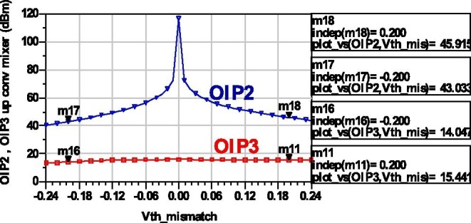
OIP2 and OIP3 versus Vth_mismatch.
Fig. 14.

Isolation between ports (a) without mismatch, (b) with Vth_mismatch = 60 mV.
4. Implication of LTI equivalent circuit for design of passive mixer-based transmitter
The above analysis aims to offer an equivalent LTI circuit as close as possible to a real differential up-conversion passive mixer with LO duty cycle = 25% for UWB transmitter. The accuracy verification of the proposed LTI model was done using the simulation results of input and output impedances as well as the conversion gain shown in Fig. 7, Fig. 9, Fig. 10. The resulting curves matches those found with LTV up-conversion passive mixer which clearly shows that the LTI model is equivalent to the actual circuit. The model proposed in Fig. 8 takes into account LO and BB harmonics, mixer input AC coupling capacitors Cbb, filter output impedance and buffer input impedance. This model is the result of analysis based on time domain equations to capture transient effects. In the simulation we used a nonzero LO rise and fall times. The maximum conversion gain is −3.68 dB. Compared to the study carried out in [14], the authors used a purely capacitive output load, they neglected the effect of input AC coupling capacitors and they assumed the LO clocks are ideal with 25% duty-cycles and zero rise and fall times.
They find a maximum conversion gain of −13 dB. One implication of having this LTI equivalent model is that designers will quickly define the reachable design space from the constraints on the performance of the mixer. Thus allowing to optimize components sizes of the up-conversion passive mixer. Using the simple LTI equivalent circuit, we can see how each design parameters impacts critical performance of the up-conversion passive mixer like input/output matching, linearity, noise and power consumption.
Another implication is that both LTI equivalent circuit of the 25% duty cycle up-conversion passive mixer in Figs. 4 and 8 can be used for different values of BB_freq, RRF, CRF, Rlpf and Ron. For medical applications using devices worn by patients and powered by battery, the transmitter must be low power. For this, the proposed mixer is the best candidate thanks to its negligible power consumption. Table 1 presents the key performances of the proposed differential 25% duty-cycle up-conversion passive mixer and compare them with published works. The proposed up-conversion passive mixer performs higher OIP3 than works in [17], [18], [19], [20], [21] while consuming only 1.5pW. Regarding conversion gain this work obtains −3.68 dB. This value is greater than the gains from passive mixers published in [13], [19]. This up-conversion passive mixer achieves the best ports isolation performances.
Table 1.
Summary of the mixer performances and comparison with reported state of the art designs.
| [13] | [17] | [18] | [19] | [20] | [21] | [22] | This work | |
|---|---|---|---|---|---|---|---|---|
| Frequency (GHz) | 0.402–0.406 | 18–28 | 2.4/5.7 | 0.9 | 10 | 0.434 | 3.1–10.6 | 3–5 |
| Conv-Gain (dB) | −5 | −2; 0.7 | 1.5/−0.2 | −3.7 | 1 | 5.4 | – | −3.68 |
| OIP3 (dBm) | 23 | 3; 5.8 | 12/13 | 13.3 | 13.6 | 7.1 | – | 15.9 |
| OP1-dB (dBm) | – | −7; −5.2 | −10.5/−9 | 5.3 | −6.2 | −0.5 | −21 | 3.912 |
| Noise Figure (dB) | – | – | – | 4 | – | – | 5.2 | |
| Technology | 0.5 µm | 0.13 µm | 0.35 µm | 0.18 µm | 0.032 µm | 0.13 µm | 0.18 µm | 0.18 µm |
| Supply Voltage (V) | 3.3 | 1.2 | 3 | 3.3 | 0.9 | 1.2 | 1.8 | 1.8 |
| Chip area | 0.135 mm2 | 0.47 mm2 | 1.1 mm2 | 0.643 mm2 | 0.086 mm2 | 0.6 mm2 | 0.02 mm2 | – |
| PDC | 23.1 mW | 8 mW | 45 mW | 29.7 mW | 15.4 mW | 0.71 mW (mixer only) | 2.4 mW | 1.5 pW (mixer only) |
| LO-RF Isolation (dB) | −24 | −30 | – | – | – | – | – | −106 |
5. Conclusion
We have presented analysis and simulation of a differential up-conversion passive mixer with 25% duty cycle intended to be used in UWB transmitter for WBAN sensor node. We proposed an equivalent LTI model of this mixer then we studied the implication of this model in the design. After that we analyzed the influence of the different design parameters on linearity, conversion gain and noise figure. We studied the impact of voltage threshold mismatch on linearity and ports isolation performances. Using the results found in this paper, RF circuit designers can quickly optimize the different parameters of the up-conversion passive mixer without going through time consuming transient simulations. This results in a guidance for optimizing low power UWB transmitter performance for WBAN applications. In particular this UWB transmitter can be used to design wireless sensors worn by corona virus patients thereby limiting patient-to-caregiver contact.
Declaration of Competing Interest
The authors declare that they have no known competing financial interests or personal relationships that could have appeared to influence the work reported in this paper.
Contributor Information
Saif Benali, Email: saifbenali.enet@gmail.com.
Hatem Trabelsi, Email: hatem.trabelsi@enis.tn.
References
- 1.IEEE standards association. IEEE Standard for Local and metropolitan area networks - Part 15.6. Wireless Body Area Networks. IEEE Std 802.15.6;(February(2)):2012.
- 2.Ryckaert J., Desset C., Fort A., Badaroglu M., De Heyn V., Wambacq P. Ultra-wideband transmitter for low-power wireless body area networks design and evaluation. IEEE Trans Circuits Syst I. 2005;52(December (12)):2515–2525. [Google Scholar]
- 3.Saputra N., Long J.R. A fully-integrated, short-range, low data rate FM-UWB transmitter in 90 nm CMOS. IEEE J Solid-State Circuits. 2011;46(July(7)):1627–1635. [Google Scholar]
- 4.Trabelsi H., Barraj I., Masmoudi M. A 3–5 GHz FSK-UWB Transmitter For Wireless Personal Healthcare Applications. Int J Electron Commun (AEÜ) 2015;69:262–273. [Google Scholar]
- 5.Ali M., Shawkey H., Zekry A., Sawan M. One Mbps 1 nJ/b 3.5–4 GHz Fully Integrated FM-UWB Transmitter for WBAN Applications. IEEE Trans Circ Syste. 2018;65(June(6)):2005–2014. [Google Scholar]
- 6.Skandar D., Farid T., Mourad L. An RF-LO current-bleeding doubly balanced mixer for IEEE 802.15.3a UWB MB-OFDM standard receivers. Int J Electron Commun (AEÜ) 2008;62:490–495. [Google Scholar]
- 7.Neda S., Abdolreza N. Design of an active CMOS subharmonic mixer with enhanced transconductance. Int J Electron Commun (AEÜ) 2017;73:98–104. [Google Scholar]
- 8.Andrews C, Molnar AC. A passive-mixer-first receiver with baseband-controlled RF impedance matching, 6 dB nf, and 27 dBm wideband IIP3. In IEEE Int. Solid-State Circuits Conf., 2010; 2010, p. 46–7.
- 9.Mirzaei A., Darabi H., Leete J., Chen X., Juan K., Yazdi A. Analysis and optimization of current-driven passive mixers in narrowband direct-conversion receivers. IEEE J Solid-State Circuits. 2009;44(October(10)):2678–2688. [Google Scholar]
- 10.Mirzaei A., Darabi H., Leete J., Chang Y. Analysis and optimization of direct-conversion receivers with 25 duty-cycle current-driven passive mixers. IEEE Trans Circuits Syst I. 2010;57(September(9)):2353–2366. [Google Scholar]
- 11.Andrews C., Molnar A.C. Implications of passive mixer transparency for impedance matching and noise figure in passive mixer-first receivers. IEEE Trans Circuits Syst I. 2010;57(December(12)):3092–3103. [Google Scholar]
- 12.He X., Sinderen J. A low-power, low-EVM, SAW-less WCDMA transmitter using direct quadrature voltage modulation. IEEE J Solid-State Circuits. 2009;44(December(12)):3448–3458. [Google Scholar]
- 13.Abraham Sánchez Gaspariano L., Annema A.-J., Muniz Montero C. Díaz Sánchez A. CMOS upconversion mixer with filterless carrier feedthrough cancelation and output power tuning. Int J Electron Commun (AEÜ) 2014;68:1224–1230. [Google Scholar]
- 14.Mirzaei A., Murphy D., Darabi H. Analysis of Direct-Conversion IQ Transmitters With 25% Duty-Cycle. Passive Mixers IEEE Trans Circuits Syst I. 2011;58(October(10)):2318–2331. [Google Scholar]
- 15.Ying Y., Bai X., Lin F. A 1-Gb/s 6–10-GHz, Filterless, Pulsed UWB Transmitter With Symmetrical Waveform Analysis and Generation. IEEE Trans Very Large Scale Integr (VLSI) Syst. 2018;26(June(6)):1171–1182. [Google Scholar]
- 16.Razavi B. Design of Analog CMOS Integrated Circuits. McGraw-Hill Series in Electrical and Computer Engineering; 2001, p. 463–81 [Chapter13, Section 13.2].
- 17.Verma A., Kenneth K.O., Lin J. A low-power up-conversion CMOS mixer for 22–29-GHz ultra-wideband applications. IEEE Trans Microw Theory Tech. 2006;54(August(8)):3295–3300. [Google Scholar]
- 18.Syu J.S., Meng C. 2.4/5.7 GHz dual-band high linearity Gilbert up-converter utilizing bias offset TCA and LC current combiner. IEEE Microw Wirel Compon Lett. 2007;17(December(12)):876–878. [Google Scholar]
- 19.Choi K., Yoo S., Kim M., Kim H., Ryu S., Kang S. CMOS DSB Transmitter With Low TX Noise for UHF RFID Reader System-on-Chip. IEEE Trans Microw Theory Tech. 2010;58(December(12)):3467–3474. [Google Scholar]
- 20.Li J., Jane Gu Q. Harmonic-based nonlinearity factorization of switching behavior in up-conversion mixers. IEEE Trans Circ Syst. 2019;66(July(7)):2468–2476. [Google Scholar]
- 21.De Xing L., Suhaidi S., Harikrishnan R., Gim Heng T. Low power upconversion mixer for medical remote sensing. Sci World J. 2014:1–5. [Google Scholar]
- 22.Baolin W., Tian C., Chao L., Weilin X., Yuanzhi Z., Xueming W. An all-digital frequency tunable IR-UWB transmitter with an approximate 15th derivative Gaussian pulse generator. Integr VLSI J. 2019;69:301–308. [Google Scholar]