

Abstract
Owing to their unique electrical and optical properties, two-dimensional transition metal dichalcogenides have been extensively studied for their potential applications in biosensing. However, simultaneous utilization of both optical and electrical properties has been overlooked, yet it can offer enhanced accuracy and detection versitility. Here, we demonstrate a dual-mode optoelectronic biosensor based on monolayer molybdenum disulfide (MoS2) capable of producing simultaneous electrical and optical readouts of biomolecular signals. On a single platform, the biosensor exhibits a tunable photonic Fano-type optical resonance while also functioning as a field-effect transistor (FET) based on a optically transparent gate electrode. Furthermore, chemical vapor deposition grown MoS2 provides a clean surface for direct immobilization of a water-soluble variant of the μ-opioid receptor (wsMOR), via a nickel ion-mediated linker chemistry. We utilize a synthetic opioid peptide to show the operation of the electronic and optical sensing modes. The responses of both modes exhibit a similar trend with dynamic ranges of four orders of magnitude and detection limits of <1 nM. Our work explores the potential of a versatile multimodal sensing platform enabled by monolayer MoS2, since the integration of electrical and optical sensors on the same chip can offer flexibility in read-out and improve the accuracy in detection of low concentration targets.
Keywords: transition metal dichalcogenides, molybdenum disulfide, multimodal biosensor, photonic crystal, field-effect transistor, mu-opioid receptor
1. Introduction
Two-dimensional materials such as graphene and transition metal dichalcogenides (TMDCs) have been widely studied as promising functional materials in various sensing devices [1–5]. Among these, as a naturally available material, MoS2 stands out as a versatile candidate due to its unique properties, namely the relatively high carrier mobility, suppressed off-state current due to a large electronic bandgap, and structural and chemical stability at ambient temperatures [6, 7]. In light of these properties, great efforts have been devoted to developing MoS2-based nanoelectronic biosensors for detecting a variety of biomolecular interactions, including DNA [8], prostate specific antigen (PSA) [2, 3, 9], and glucose [4]. Most of these biosensors operate in a single mode, particularly in a field-effect transistor (FET) configuration, utilizing the changes in channel conductivity and consequently the tranduced electrical output as a result of binding or adsorption of target molecules. These binding events occuring near the surface also produce perturbations in the local dielectric permittivity enabling detection via electromagnetic means, which have been elusive. To this end, by coupling MoS2 with a nanostructure exhibiting photonic resonances [ 10–12], one can realize a versatile multimodal sensor capable of interrogating biomolecular interactions with simultaneously transduced electrical and optical signals in one single device platform.
Multimodal biosensors can potentially improve the overall accuracy of detection by comparing results from different mechanisms, obtaining multiple characteristics of a biomolecular binding event, and providing flexibility for operation in different situations. Previous works have incorporated the two modes by fabricating plasmonic nanostructures on a TMDC surface [13], such that the device exhibits a photonic resonance that spectrally shifts upon attachment of target molecules [14, 15]. The integration of graphene [14] or carbon nanotubes [15] into traditional devices have been demonstrated to enable parallel transduction of electronic, optical, and even mechanical signals. However, 2D materials in these devices merely act as a transparent substrate in the optical mode, playing no active role in optical transduction.
Here, we experimentally demonstrate a dual-mode biosensor as shown schematically in figures 1(a) and (b). By integrating MoS2 monolayers on a dielectric photonic crystal (PhC) slab with an optically transparent gate electrode, MoS2 takes an active part in both electrical and optical detection of DAMGO ([D-Ala2, N-MePhe4, Gly-ol]-enkephalin), a synthetic opioid peptide and specific MOR agonist. We choose CVD-grown MoS2 as the active material because the large (>50 μm lateral size) and dense crystals make it suitable for large scale fabrication of devices [16, 17]. In this device, monolayer MoS2 plays critical roles as a functionalization layer for nanophotonic sensing and FET channel for nanoelectronic sensing.
Figure 1.
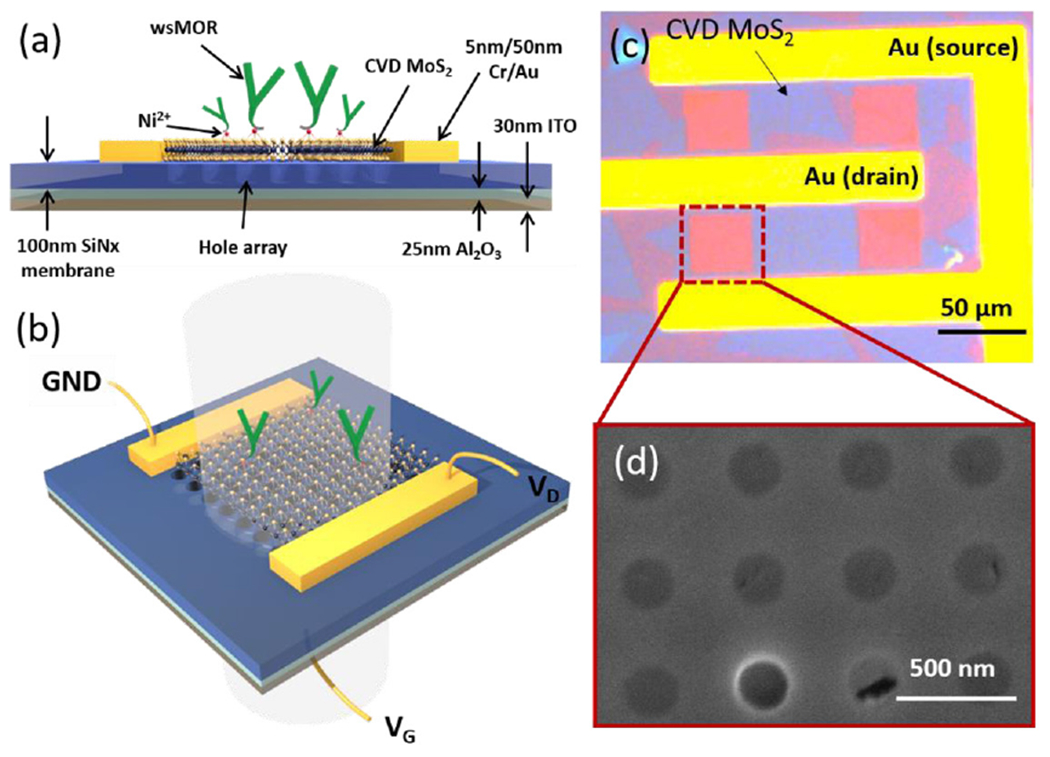
Device structure and sensing scheme. (a) The biosensor was fabricated on a freestanding 100 nm-thick SiN membrane supported by a Si frame. On the backside of the membrane are 25 nm Al2O3 and 30 nm ITO. Photonic crystal slabs were fabricated directly on the SiN membrane between two Cr/Au electrodes. Large CVD MoS2 flakes were transferred over the two electrodes and photonic crystals to create an FET and optical modulator on the same platform. (b) Sensing scheme of the dual-mode sensor with VG and VD connected to the gate and drain electrode, respectively, with the source electrode as a common ground. The nanohole arrays have a period of 440 nm and hole radius of 120 nm, giving rise to a Fano resonance at ~700 nm for refractive index sensing. (c) Microscope image of a device. Purple-ish blue regions are the overlaying CVD MoS2. (d) SEM of a PhC hole array with the superimposing monolayer CVD MoS2.
MoS2 can be directly functionalized with a synthetic water soluble μ-opioid receptor, wsMOR [18], via Ni2+ linkers [19]. Monolayer MoS2 exhibits a pristine surface with no dangling bonds, making direct functionalization difficult. Yet, proximity of binding events to the active surface is one of the factors that determines the sensitivity of a biosensor. Most MoS2-based biosensors rely on a silanized top dielectric layer (e.g. APTES functionalization), such as Al2O3 and HfO2 films [1, 3, 9], to bind protein probes. This limits the probe-target interactions to occur several nanometers away from the active MoS2 surface, reducing the expected device sensitivity. The direct functionalization method used here utilizes Ni2+ ions adsorbed on the MoS2 surface to bind to the histidine tag on the wsMOR protein [20]. This allows the receptor-target interactions to take place very close to the surface of monolayer MoS2.
As shown in figure 1(c), CVD-grown MoS2 flakes are placed over an array of nanoholes on a 100 nm thick suspended silicon nitride (SiN) membrane. Figure 1(d) shows a scanning electron micrograph (SEM) of a MoS2-integrated square lattice hole array that makes up a PhC slab patterned lithographically between two electrodes. This PhC nanostructure exhibits optical Fano resonances which are characterized by their asymmetric line shape observable in the transmission spectra [21]. The spectral position of these Fano resonances are highly sensitive to small changes in the local permittivity in the surrounding medium. This enables sensitive optical detection of biomolecular interactions via refractive index modulation [22]. On this device, the accumulation of target molecules on monolayer MoS2 induces an effective increase in the refractive index surrounding the PhC slab, causing the Fano resonance peak to redshift by Δλ. We employ this spectral shift in the optical transmission spectra to quantify the concentration of target molecules.
Simultaneously, bound molecules modify the in-plane conductivity via electrostatic gating effects, which can be detected as a change in the channel source-drain current (ΔIDS). Figure 1(c) shows a mechanically transferred MoS2 monolayer covering the drain and source electrodes, creating a semiconducting channel. To enable nanoelectronic sensing, 25 nm alumina (Al2O3) and 30 nm indium tin oxide (ITO) films are deposited on the backside of the SiN PhC slab as optically transparent dielectric and back gate electrode, respectively. These crucially enable the device to support two independent modes of sensing on the same chip. Since the PhC hole arrays are etched through the SiN slab, the underlying Al2O3 film maintains physical and electrical isolation between MoS2 and the ITO back gate. As a result, the device exhibits field-effect characteristics while remaining optically transparent to allow transmission measurements.
2. Results and discussions
Having described the physical mechanisms involved in our sensor, we illustrate in figure 1(b) the dual-mode operation of the device. In the FET or nanoelectronic mode, two electrical sourcemeters (Keithley 2400) were connected, respectively, to the back-gate (VG) and drain (VD) electrodes with the source electrode acting as the common ground. We first verified that the presence of the nanoholes on the SiN membrane did not have a significant effect on the FET characteristics. To do this, we fabricated two devices, one with PhC hole arrays etched through the SiNx membrane and one without. We then measured the gate-source current (IGS, through ITO/Al2O3/SiN/MoS2) as a function of VG as shown in figure 2(a). The two devices displayed similar IGS dependence on VG, indicating that the hole arrays etched into the SiN dielectric layer did not inhibit the nanoelectric operation. The thin Al2O3 layer here is the key component in providing excellent electrical insulation between regions of MoS2 suspended over nanoholes and bottom ITO back gate electrode. Without the Al2O3 layer, suspended monolayers can sag and come into contact with ITO under bias, which leads to electrical shorting through the structure. While this multilayer dielectric configuration provides electrical insulation on par with SiN, we still need to determine the range of voltages for which there is no dielectric breakdown for reliable operation of the dual-mode sensor. Experimental results in figure 2(a) show that the leakage current IGS increases exponentially when VG is larger than 10 V indicating the onset of electrical breakdown. For VG > 20 V, the capacitor structure can experience irreversible dielectric breakdown [23]. Therefore, for device characterization and sensing experiments, we limit the operation of the dual-mode sensor to gate voltages between VG = −2 V and 5 V.
Figure 2.

Optoelectronic device characterization. (a) Comparison between IGS–VG curves for the device with and without PhC hole arrays. (b) IGS–VD and (c) IDS–VD characteristics for the MoS2-based FET. (d) Simulated FDTD transmission spectra of MoS2 on an unpatterned (red) and patterned (blue) substrate. The substrate is a 100 nm-thick suspended SiN slab with 25 nm Al2O3 and 30 nm ITO layers on the backside. The red curve shows a slowly varying Fabry–Perot resonance due to the slab substrate. Small peaks at 650 nm and 610 nm are due to the absorption of A- and B-excitons, respectively. Patterned substrate consists of a rectangular array of nanoholes etched only through the SiN slab. The blue curve shows peaks at 690 nm and 600 nm corresponding to the first and second order Fano resonances, respectively. These resonances arise from the hybridization of 2nd order grating scattering from the nanohole array and the Fabry–Perot transmission background. (e) Measured transmission spectra for the fabricated structure. Additional peaks are attributed to nonuniformities in the fabrication process.
Next, we examined the transfer characteristics, IDS–VG and IDS–VD, of the MoS2 FET. As shown in the IDS–VG curve in figure 2(b), we swept VG from −2 V to 5 V at 1 V sℒ1 while keeping VD constant, and measured IDS across the electrodes. As expected, IDS increased exponentially with VG when the device is in the on-state and increasing VD increases the channel current IDS. In figure 2(c), we fixed VG to obtain a relationship between IDS and VD. Device drain current IDS increased linearly with VD in the linear region and plateaued when the FET entered the saturation region at higher VD bias. The IG–VDS and ID–VDS characteristics of our device is in good agreement with those of the previosly reported MoS2-based FETs [24–26].
In the optical or nanophotonic mode, the presence of hole arrays on a suspended SiN slab gives rise to Fano guided mode resonances that can be observed via transmission measurements. Upon illumination on a SiN PhC slab, a portion of the incident light is transmitted through the uniform slab, generating a slowly varying Fabry–Perot background (red line in figure 2(d)). This hybridizes with the remaining portion of light that excites the in-plane narrow-band guided resonance, produced by a periodic modulation in the dielectric constant over the square lattice hole array. As a result of this interference, we observe sharp Fano-type resonances in the transmission spectra characterized by their asymmetric spectral lineshapes [27]. The spectral positions of these Fano resonances can be tuned by varying the geometric parameters of the photonic crystal, such as the period and diameter of the holes.
We designed the photonic crystal to exhibit a Fano resonance at ~700 nm, spectrally away from the MoS2 A-exciton absorption peak at 650 nm in order to minimize optical losses. Figure 2(d) shows the finite difference time domain (FDTD) method simulated transmission spectrum of a PhC consisting of a square array of holes with a radius of 120 nm and array period of 440 nm. The structure exhibits a Fano resonance at 690 nm with a theoretical quality (Q)-factor of about 60. The small spectral dip at ~650 nm corresponds to the A-exciton absorption peak of MoS2 [28]. For transmission spectrum measurements, a collimated white light source was incident on the PhC and the transmitted light was collected through a microscope objective. Figure 2(e) shows the measured transmission spectra for the fabricated structure having the same PhC parameters, with and without the MoS2 monolayer. The spectral peaks here are in good agreement with the FDTD simulations, with the A-exciton peak at 650 nm and the first and second Fano resonances at ~700 nm and 600 nm, respectively. Additional peaks in the measured spectra are attributed to nonuniformities introduced by the fabrication process.
To demonstrate the nanoelectric and nanophotonic sensing operation in this work, we utilized a histidine-tagged water soluble variant of the μ-opioid peptide receptor (MOR) and synthetic target opioid peptide analogue to encephalin. The native MORs are a class of opioid receptors that possess a high affinity for endogenous ligands such as enkephalin and beta-endorphin [29]. Enkephalin is a neuropeptide which serves as an important signaling molecule in the brain [30]. Sensitive detection of opioid peptides is useful in drug discovery and development [19].
To achieve a clean surface for functionalization, a low temperature transfer method was employed as described in the methods section. This allows the PMMA layer to readily dissolve in acetone without leaving any residues on the MoS2 surface. Atomic force microscope (AFM) images of MoS2 surfaces before and after transfer in are shown figure S1 (supplementary information (stacks.iop.org/TDM/7/014004/mmedia)). These confirm that the low temperature method yields a clean MoS2 surface with very few residues. If a significant number of residues was present, functionalization would result in a lower density of immobilized probes available for detection, which would deteriorate the linear range, sensitivity, and limit of detection of the biosensor [31]. PMMA residues can also induce unintentional doping effects and scattering loss in the nanoelectronic and nanophotonic operation, respectively, which would further degrade the detection sensitivity of the sensor [32].
Figure 3(a) illustrates the functionalization scheme for wsMOR on MoS2 via Ni2+ linkers. To functionalize MoS2, we first placed droplets of 5 mM NiCl2 solution onto the device and let incubate for 1 h. In this step, Ni2+ ions formed coordinate bonding with sulfer atoms on the surface of MoS2. The sample was immersed in a water bath for 5 min followed by another water bath for 20 min to remove any excess Ni2+ ion. Next, droplets of 10 μM wsMOR in a buffer solution were placed on the device array for 1 h, allowing the histidine tag to bind to Ni2+. Finally, the sample was left in a water bath for 5 min to wash off unbound receptors and blown dry.
Figure 3.

MoS2 functionalization. (a) Schematic for the linker chemistry for direct functionalization. The red atom represents Ni2+ that is bound to the sulfur atoms on MoS2 via coordinate bonds. The white region on wsMOR represents the histidine tag that binds preferentially to the Ni2+ ions. (b) SEM of wsMOR-functionalized MoS2. (c) AFM topographic image of unfunctionalized transferred CVD MoS2 on SiO2, (d) wsMOR-functionalized MoS2 on SiO2. (e) and (f) Height profiles of the line scan shown in (c) and (d), respectively.
After functionalization, the immobilization of wsMOR was verified via atomic force microscopy. An SEM of a functionalized MoS2 monolayer is shown in figure 3(b). Figures 3(c) and (d) show the surface morphology of MoS2 flakes before and after functionalization, respectively, indicating uniform protein coverage. The surface of transferred MoS2 was uniform and relatively flat. The flake thickness was about ~1 nm (figure 3(e)) which agrees well with the reported AFM measurements of CVD-grown monolayer MoS2 [16, 33, 34]. After functionalization with Ni2+ and wsMOR protein, the thickness of MoS2 flakes uniformly increased to ~3 nm (figure 3(f)). This change is consistent with the 46 kDa size of wsMOR [20]. The surface of the substrate remained flat and featureless which indicates specific attachment of wsMOR on MoS2 surface only. This mechanism of protein attachment on MoS2 allows binding of target molecules to occur very close to the sensing surface.
As a result of wsMOR functionalization, the drain current of the device increased by ~8 times, indicating an increase in channel conductance (figure 4(a)). The hysteretic behavior between the forward and backward voltage sweeps are attributed to adsorption of ambient molecules on the surface of MoS2 and charge trapping between the monolayer and substrate [35]. We note that the functionalization process may either increase or decrease MoS2 channel conductance depending on the quality and initial doping of the MoS2 flakes. Meanwhile, the Fano resonance red-shifted by 3 nm due to the increased refractive index surrounding the MoS2-integrated PhC slab (figure 5(a)).
Figure 4.

Nanoelectronic sensing. (a) IDS–VG characteristics of the sensor pre-functionalization (black), after functionalization with wsMOR (red), and after exposure to 10 μM DAMGO (blue). VD = 0.1 V. (b) Electronic response reported as percentage change in IDS with respect to the IDS of wsMOR-functionalized device, extracted from IDS–VG curve at VG = 2.5 V. Error bars represent the standard deviation of the mean between three repeated measurements. The experimental data was fitted by the Langmuir–Hill isotherm to obtain the sensor calibration curve for the nanoelectronic mode (red). (c) Normalized electronic response of three different devices.
Figure 5.

Nanophotonic sensing. (a) Transmission spectra of the sensor pre-functionalization (black), after functionalization with wsMOR (red), and after exposure to 10 μM DAMGO (blue). (b) Optical response reported as resonance wavelength shift with respect to the resonance peak position of wsMOR-functionalized device. Error bars represent the standard deviation of the mean between three repeated measurements. The experimental data was fitted by the Langmuir-Hill isotherm to create the sensor calibration curve for the nanophotonic mode (blue). (c) Normalized optical response of three devices.
Dual-mode sensing experiments were carried out with target DAMGO synthetic opioid peptide diluted in deionized water. To test the sensor response, we exposed the device to target DAMGO in DI water at different concentrations, ranging from 0.1 nM to 10 μM. For each concentration, droplets of target DAMGO solution were placed on the device for 30 min. Then the device was rinsed in a DI water bath for 2 min and blown dry with a nitrogen gun. We note that we do not expect the target DAMGO to bind to the Ni2+ linkers as they do not contain histidine residues (Ni2+ binding sites) as in the histidine-tagged wsMOR [36]. Therefore, a blocking agent was not necessary to deactivate the linker ions.
Current and transmission measurements were carried out sequentially at each concentration to obtain the dual-mode sensor responses. The dual-mode sensing responses as a function of DAMGO concentration are presented in figures 4(b) and 5(b), respectively, as a percent change in channel current, ΔIDS/I0, and resonance peak shift, Αλ, with respect to responses of the functionalized device. For nanoelectronic sensing, we swept VG from −2 V to 5 V at 1 V s−1 and a constant VD of 0.1 V. This small value of VD were used to keep the channel current small in order to avoid any heating effects. The current responses for different DAMGO concentrations were extracted at VG = 2.5 V, half way between the turn on voltage and maximum voltage applied. For nanophotonic sensing, the measured transmission spectra were first fitted near the first Fano resonance. The peak positions were then obtained from the fit for each DAMGO concentration. Both curves were fitted by the Langmuir-Hill equation
where θ = ΔIDS/IDS,0 or Δλ is the sensor response representing the fraction of wsMOR that is bound to DAMGO, [C] is the DAMGO concentration, Ka is the DAMGO concentration that produces half of the maximum response, A is the maximum response, Z is the offset response, and n is the Hill coefficient. The dissociation constant describing binding affinity is described as Kd = (Ka)n.
Responses in both modes exhibit similar trend as they scale with the fraction of conjugated wsMOR on MoS surface. The electrical response in figure 4(b) is fitted with Ka = 1.2 nM, A = 145 and n = 0.87, and the optical response in figure 5(b) with Ka = 1.0 nM, A = 1.86, and n = 0.91. Figures 4(c) and 5(c) show normalized response of three devices. We extracted averaged fitting parameters to be Ka = 1.5 ± 0.4 nM and n = 0.87 ± 0.01 for the nanoelectronic response, and Ka = 1.2 ± 0.2 nM and n = 0.89 ± 0.02 for the nanophotonic response. These yield the dissociation constants, Kd, for DAMGO-wsMOR interaction of 3.6 ± 0.5 nM and 2.5 ± 0.8 nM as obtained via electronic and optical modes, respectively. These values are also in good agreement with previously reported Kd, of MOR for DAMGO [37, 38]. Despite using different transduction mechanisms, we found the two Kd values to be remarkably close. This evidently demonstrates the independent operation of the two systems, allowing us to consistently probe biomolecular binding events via two distinct physical mechanisms on the same device.
For both modes, the limit of detection is about 0.1 nM as limited by electrical noise and the spectral resolution of the instrument. Since the sensor responses both scale with surface coverage of the target peptide, the linear range of the sensor is approximately 0.1–10 nM for both modes of operations. The sensitivity of the sensor is extracted from the slope of the fit in the linear range, yielding the sensitivity as a percent change of drain current per unit target concentration of 10.5% nM−1, and spectral displacement per unit concentration of 0.15 nm nM−1. We also note that the sensing area and photonic crystal design on this device can be independently optimized further to improve the sensitivity while maintaining dual-mode operation. The combination of two sensing modes can further improve the accuracy of detection by reducing the margin of errors in the individual sensor responses, and provide great flexibility in modes of operation.
3. Conclusion
In summary, we demonstrate here a dual-mode optoelectronic biosensor based on CVD-grown monolayer MoS2 as an active multifunctional element. The device is composed of a MoS2-based FET fabricated on a SiN PhC slab exhibiting an optical Fano resonance. ITO back gate electrode and Al2O3 dielectric layer keep the device transparent for transmission measurements, and prevent electrical shorting through the nanoholes. These allow the device to support two modes of sensing simultaneously. The monolayer MoS2 acts as a protein immobilization surface, active functionalization layer for nanophotonic refractive index sensing via Fano resonance tuning, and FET channel for nanoelectronic sensing. With our present design, the percent yield of working devices is about 70%, due to the flakes having to both bridge two electrodes and cover a photonic crystal hole array. We note that a different device layout could increase the yield further. Our previous work demonstrated a large scale production of similar FET biosensors using CVD-grown MoS2, achieving a yield of over 90% [20]. Therefore our proof-of-concept demonstration of the dual mode sensor can readily be extended to large area fabrication with reasonably high yield in the future. To demonstrate dual-mode operation, the sensor was functionalized with wsMOR, and used to determine the affinity of DAMGO as a function of concentration via electrical and optical measurements. The sensor responses were read out in terms of percent change in drain current IDS and wavelength shift for the Fano resonance in the nanoelectronic and nanophotonic modes, respectively. Both responses agreed well with the Langmuir–Hill model for ligand-receptor binding and exhibited binding constants within the same range as those previously reported in literature using radio-active materials. This approach not only avoids using radio-active materials, but also combining two readouts can increase the accuracy of results by reducing uncertainty that arises from each individual mode, such as calibration and systematic errors. The design can potentially be optimized to provide extensive measurements of biomolecular processes, improved dynamic sensing range and sensitivity and flexibility in mode of operation. Our work shows that the unique physical, chemical, electronic and optical properties of monolayer MoS2 can open up new opportunities for the design of multimodal biosensors.
4. Methods
4.1. Device fabrication
An array of devices were fabricated on a freestanding 100 nm-thick silicon nitride membrane (Norcada), which provided a transparent substrate for transmission measurements. First, 20 nm Al2O3 was grown on the backside of the substrate by atomic layer deposition (ALD) at 200 °C. This was followed by deposition of 30 nm ITO by RF sputtering. Next, we used photolithography to pattern electrodes on the front side of the substrate; 5 nm Cr and 50 nm Au were deposited via electron-beam evaporation and lifted off to form electrodes. Hole arrays were patterned in between electrodes on the SiN membrane via electron-beam lithography. The holes were formed by dry etching through the SiN slab via reactive ion etching (RIE) with O2 and CHF3 gases with Al2O3 layer on the back side acting as an etch stop layer.
4.2. CVD MoS2 transfer
After the electrodes and hole arrays were fabricated, flakes of CVD-grown MoS2 were transferred onto the devices by wet transfer. We first spin-coated PMMA (500 nm–1 μm thick) on as-grown MoS2 flakes on a SiO2/Si substrate. Next, the sample was left floating in a bath of 0.1 M NaOH to etch SiO2, releasing the PMMA film from the underlying substrate. The floating PMMA film was carefully scooped up with a glass slide and released in three sequential DI water baths to wash off any NaOH. The PMMA film was then scooped up from the last water bath with the patterned SiN membrane chip, and the sample was blown dry with a N2 gun until the water droplets visually disappeared. Then the sample was left to further dry in a dessicator for at least 2 h. To remove PMMA, the sample was submerged in an acetone bath for 30 min, followed by a second acetone bath for 1 h. Finally, the sample was placed in an IPA bath for 10 min to remove acetone and blown dry. The finished device underwent a current annealing process prior to measurements. With constant VG = 10 V, VD was slowly increased from 0.1 V to 3 V and left for 2 min. Prior to sensing experiments, transferred MoS2 flakes on the device were functionalized with wsMOR as described in main text.
Supplementary Material
Acknowledgments
This work was supported by NSF under the NSF 2-DARE Program (EFMA-1542879), and NIH R01 (1R01GM111421, PI, RL).
Footnotes
Supplementary material for this article is available online
References
- [1].Sarkar D, Liu W, Xie X, Anselmo AC, Mitragotri S and Banerjee K 2014. MoS2 field-effect transistor for next-generation label-free biosensors ACS Nano 8 3992–4003 [DOI] [PubMed] [Google Scholar]
- [2].Lee J, Dak P, Lee Y, Park H, Choi W, Alam MA and Kim S 2015. Two-dimensional layered MoS2 biosensors enable highly sensitive detection of biomolecules Sci. Rep 4 7352. [DOI] [PMC free article] [PubMed] [Google Scholar]
- [3].Wang L, Wang Y, Wong JI, Palacios T, Kong J and Yang HY 2014. Functionalized MoS2 nanosheet-based field-effect biosensor for label-free sensitive detection of cancer marker proteins in solution Small 10 1101–5 [DOI] [PubMed] [Google Scholar]
- [4].Shan J, Li J, Chu X, Xu M, Jin F, Wang X, Ma L, Fang X, Wei Z and Wang X 2018. High sensitivity glucose detection at extremely low concentrations using a MoS2-based field-effect transistor RSC Adv. 8 7942–8 [DOI] [PMC free article] [PubMed] [Google Scholar]
- [5].Radisavljevic B, Radenovic A, Brivio J, Giacometti V and Kis A 2011. Single-layer MoS2 transistors Nat. Nanotechnol 6 147–50 [DOI] [PubMed] [Google Scholar]
- [6].Wang QH, Kalantar-Zadeh K, Kis A, Coleman JN and Strano MS 2012. Electronics and optoelectronics of two-dimensional transition metal dichalcogenides Nat. Nanotechnol 7 699–712 [DOI] [PubMed] [Google Scholar]
- [7].Jariwala D, Sangwan VK, Lauhon LJ, Marks TJ and Hersam MC 2014. Emerging device applications for semiconducting two-dimensional transitional metal dichalcogenides ACS Nano 8 1102–20 [DOI] [PubMed] [Google Scholar]
- [8].Mei J, Li YT, Zhang H, Xiao MM, Ning Y, Zhang ZY and Zhang GJ 2018. Molybdenum disulfide field-effect transistor biosensor for ultrasensitive detection of DNA by employing morpholino as probe Biosens. Bioelectron 110 71–7 [DOI] [PubMed] [Google Scholar]
- [9].Park H et al. 2017. Label-free and recalibrated multilayer MoS2 biosensor for point-of-care diagnostics ACSAppl. Mater. Interfaces 9 43490–7 [DOI] [PubMed] [Google Scholar]
- [10].Zhang W, Ganesh N, Block ID and Cunningham BT 2008. High sensitivity photonic crystal biosensor incorporating nanorod structures for enhanced surface area Sens. Actuators B 131279–84 [Google Scholar]
- [11].Guo Y, Ye JY, Divin C, Huang B, Thomas TP, Baker JR Jr. and Norris TB 2010. Real-time small molecule binding detection using a label-free photonic crystal biosensor Anal. Chem. proceeding 82 5211–8 [DOI] [PMC free article] [PubMed] [Google Scholar]
- [12].Inan H, Poyraz M, Inci F, Lifson MA, Baday M, Cunningham BT and Demirci U 2017. Photonic crystals: emerging biosensors and their promise for point-of-care applications Chem. Soc. Rev 46 366–88 [DOI] [PMC free article] [PubMed] [Google Scholar]
- [13].Butun S, Palacios E, Cain D, Liu Z, Dravid VP and Aydin K 2017. Quantifying plasmon-enhanced light absorption in monolayer WS2 films ACS Appl. Mater. Interfaces 9 15044–51 [DOI] [PubMed] [Google Scholar]
- [14].Zhu AY, Yi F, Reed JC, Zhu H and Cubukcu E 2014. Optoelectromechanical multimodal biosensor with graphene active region Nano Lett. 14 5641–9 [DOI] [PubMed] [Google Scholar]
- [15].Oh J, Chang YW, Kim HJ, Yoo S, Kim DJ, Im S, Park YJ, Kim D and Yoo KH 2010. Carbon nanotube-based dual-mode biosensor for electrical and surface plasmon resonance measurements Nano Lett. 10 2755–60 [DOI] [PubMed] [Google Scholar]
- [16].Lee Y-H et al. 2012. Synthesis of large-area MoS2 atomic layers with chemical vapor deposition Adv. Mater 24 2320–5 [DOI] [PubMed] [Google Scholar]
- [17].Smithe KKH, Suryavanshi SV, Muñoz Rojo M, Tedjarati AD and Pop E 2017. Low variability in synthetic monolayer MoS2 devices ACS Nano 11 8456–63 [DOI] [PubMed] [Google Scholar]
- [18].Zhao X, Perez-Aguilar JM, Matsunaga F, Lerner M, Xi J, Selling B, Johnson ATC, Saven JG and Liu R 2014. Characterization of a computationally designed water-soluble human μ-opioid receptor variant using available structural information Anethesiology 121 866–75 [DOI] [PMC free article] [PubMed] [Google Scholar]
- [19].Lerner MB et al. 2014. Scalable production of highly sensitive nanosensors based on graphene functionalized with a designed G protein-coupled receptor Nano Lett. 14 2709–14 [DOI] [PMC free article] [PubMed] [Google Scholar]
- [20].Naylor CH, Kybert NJ, Schneier C, Xi J, Romero G, Saven JG, Liu R and Johnson ATC 2016. Scalable production of molybdenum disulfide based biosensors ACS Nano 10 6173–9 [DOI] [PMC free article] [PubMed] [Google Scholar]
- [21].Limonov MF, Rybin MV, Poddubny AN and Kivshar YS 2017. Fano resonances in photonics Nat. Photon 11 543–54 [Google Scholar]
- [22].Wu C, Khanikaev AB, Adato R, Arju N, Yanik AA, Altug H and Shvets G 2011. Fano-resonant asymmetric metamaterials for ultrasensitive spectroscopy and identification of molecular monolayers Nat. Mater 11 69–75 [DOI] [PubMed] [Google Scholar]
- [23].Yi F, Shim E, Zhu AY, Zhu H, Reed JC and Cubukcu E 2013. Voltage tuning of plasmonic absorbers by indium tin oxide Appl. Phys. Lett 102 221102 [Google Scholar]
- [24].Tong X, Ashalley E, Lin F, Li H and Wang ZM 2015. Advances in MoS2-based field effect transistors (FETs) Nano-Micro Lett. 7 203–18 [DOI] [PMC free article] [PubMed] [Google Scholar]
- [25].Xie X, Sarkar D, Liu W, Kang J, Marinov O, Deen MJ and Banerjee K 2014. Low-frequency noise in bilayer MoS2 transistor ACS Nano 8 5633–40 [DOI] [PubMed] [Google Scholar]
- [26].Schmidt H et al. 2014. Transport properties of monolayer MoS2 grown by chemical vapour deposition Nano Lett. 14 1909–13 [DOI] [PubMed] [Google Scholar]
- [27].Huang M, Yanik AA, Chang T and Altug H 2009. Sub-wavelength nanofluidics in photonic crystal sensors Opt. Express 17 24224–33 [DOI] [PubMed] [Google Scholar]
- [28].Splendiani A, Sun L, Zhang Y, Li T, Kim J, Chim C, Galli G and Wang F 2010. Emerging photoluminescence in monolayer MoS2 Nano Lett. 10 1271–5 [DOI] [PubMed] [Google Scholar]
- [29].Ping J, Vishnubhotla R, Xi J, Ducos P, Saven G, Liu R and Johnson ATC 2018. All-electronic quantification of neuropeptide-receptor interaction using a bias-free functionalized graphene microelectrode ACS Nano 12 4218–23 [DOI] [PMC free article] [PubMed] [Google Scholar]
- [30].Frederickson RC 1977. Enkephalin pentapeptides—a review of current evidence for a physiological role in vertebrate neurotransmission Life Sci. 21 23–42 [DOI] [PubMed] [Google Scholar]
- [31].Chen T, Thi P, Loan K, Hsu C, Lee Y, Wang JT, Wei K, Lin C and Li L 2013. Label-free detection of DNA hybridization using transistors based on CVD grown graphene Biosens. Bioelectron 41 103–9 [DOI] [PubMed] [Google Scholar]
- [32].Liang J, Xu K, Toncini B, Bersch B, Jariwala B, Lin Y-C, Robinson J and Fullerton-Shirey SK 2019. Impact of post-lithography polymer residue on the electrical characteristics of MoS2 and WSe2 field effect transistors Adv. Mater. Interfaces 6 1801321 [Google Scholar]
- [33].He G et al. 2015. Conduction mechanisms in CVD-grown monolayer MoS2 transistors: from variable-range hopping to velocity saturation Nano Lett. 15 5052–8 [DOI] [PubMed] [Google Scholar]
- [34].Wang S, Rong Y, Fan Y, Pacios M, Bhaskaran H, He K and Warner JH 2014. Shape evolution of monolayer MoS2 crystals grown by chemical vapor deposition Chem. Mater 26 6371–9 [Google Scholar]
- [35].Late DJ, Liu B, Matte HSSR, Dravid VP and Rao CNR 2012. Hysteresis in single-layer MoS2 field effect transistors ACS Nano 6 5635–41 [DOI] [PubMed] [Google Scholar]
- [36].Bornhorst J A and Falke JJ 2000. [16] Purification of proteins using polyhistidine affinity tags Methods Enzymol. 326 245–54 [DOI] [PMC free article] [PubMed] [Google Scholar]
- [37].Chen ZR, Irvine RJ, Somogyi AA and Bochner F 1991. Mu receptor binding of some commonly used opioids and their metabolites Life Sci. 48 2165–71 [DOI] [PubMed] [Google Scholar]
- [38].Volpe DA, Mcmahon GA, Mellon RD, Katki AG, Parker RJ, Colatsky T, Kropp TJ and Verbois SL 2011. Uniform assessment and ranking of opioid Mu receptor binding constants for selected opioid drugs Regul. Toxicol. Pharmacol 59 385–90 [DOI] [PubMed] [Google Scholar]
Associated Data
This section collects any data citations, data availability statements, or supplementary materials included in this article.