

Abstract
Band-to-band tunneling field-effect transistors (TFETs)1–7 have emerged as promising candidates to replace conventional metal-oxide-semiconductor field-effect transistors (MOSFETs) for low-power integration circuits and have been demonstrated to overcome the thermionic limit, that results intrinsically in subthreshold swings of at least 60 mV/dec at room temperature1,5,6. Here we demonstrate TFETs based on few-layer black phosphorus, in which multiple top gates create electrostatic doping in the source and drain regions. By electrically tuning the doping types and levels in the source and drain regions, the device can be reconfigured to allow for TFET or MOSFET operation and can be tuned to be n-type or p-type. Full band atomistic quantum transport simulations of the fabricated devices agree quantitatively with the I-V measurements which gives credibility to the promising simulation results of ultra-scaled phosphorene TFETs8,9. Using atomistic simulations, we project substantial improvements in the performance of the fabricated TFETs when channel thicknesses and oxide thicknesses are scaled down.
In recent years, two-dimensional (2D) semiconducting materials have attracted attention as channel material for next-generation transistors10–15, as the ultra-thin body allows for ideal electrostatic control of the channel potential, addressing problems in conventional devices related to channel length scaling16–18. However, regardless of the actual channel material, in conventional MOSFETs the current flowing below threshold is always controlled by thermionic emission over the gate controlled barrier between source and drain, which fundamentally limits the subthreshold swing (SS) to about 60 mV/dec at room temperature. Among other things, this hinders scaling down the supply voltage and prevents further, urgently needed, reduction in power dissipation. Therefore, apart from new materials for transistor applications in general, novel devices based on alternative switching mechanisms are required to break the thermal limit and to achieve ultra-low-power device operation. Band-to-band tunneling (BTBT) field-effect transistors (TFETs)1,2,4 have been proposed and demonstrated as promising candidates for achieving steep-slope devices. Combining this concept with using 2D materials as the active channel in TFETs allows benefitting from the ultra-thin body thickness aspect of 2D, which leads to short tunneling distances. Small tunneling distances in turn result in both, high ON-state currents (ION) and steep SS values19–21. Various research articles on building TFETs using 2D materials have been published over the last years. Most of this work focused on 2D vertical heterojunctions, such as germanium (Ge)/bilayer molybdenum disulfide (MoS2)6, tin diselenide (SnSe2)/BP22 and SnSe2/tungsten diselenide (WSe2)23. Some19,24,25 studied homojunction TFETs based on WSe2, a 2D material intensively evaluated for TFET applications19,20. However all these tunneling devices suffer from low current levels. To evaluating the on-current ION for TFETs, it is instructive to take a look at the transmission probability T, that describes charge transport through the BTBT barrier, based on the Wentzel–Kramer–Brillouin (WKB) approximation26,27:
| (1) |
where Eg is the bandgap, m* is the tunneling effective mass, and λ is the screening length. In order to achieve a high transmission probability, Eg and m* need to be minimized by choosing a suitable material and λ needs to be reduced by improving the electrostatics in the device. TFETs built from WSe2 exhibit thus unavoidably low ION-values, since the large bandgap28 (1.0 eV to 1.5 eV) and high effective masses14 (me* = 0.34 m0, mh* = 0.44 m0) of WSe2 give rise to a low transmission probability. On the other hand, black phosphorus (BP) as channel material is characterized by a tunable small bandgap15 (0.3 eV to 1.5 eV) and low effective mass29 (0.15 m0) and can thus be expected to be a better material choice for high on-current TFET applications8,30. Based on few-layer BP, here we report experimental results on a lateral TFET, with BTB tunneling occurring at electrostatically defined p/n (or n/p) homojunctions that can be controlled by means of multiple gates, and that we call correspondingly Reconfigurable-Electrostatically-Doped Tunneling Field-Effect Transistor (BP RED-TFET).
Figure 1a and 1b show the schematic and a scanning electron microscopy (SEM) image (false-colored for clarity) of a BP RED-TFET. A few-layer BP flake is located on top of Au source/drain contacts, and two top-gates overlapping with the source and drain electrodes, G1 and G2, can be used to induce the desired electrostatic doping in the source and drain portions (next to the contact electrodes) of the BP, while the middle top-gate G controls the channel region. Devices employed in this study have varying flake thicknesses as measured by AFM between 8nm and 13nm. Figure 1c shows a representational cross-section high-angle annular dark field (HAADF) scanning transmission electron microscopy (STEM) image of the BP RED-TFET cross-section cut along the A-A’ line depicted in Figure 1b. The triple-gate structure of the device is clearly visible in the low-magnification image; the high-magnification details (images below) show the interface of BP with the gate oxide and the crystalline structure of BP. Note that there are amorphous-like layers both on the top and on the bottom of the BP layer, presumably POx (Supplementary Figures S1d–S1g). These unexpected layers not only reduce the thickness of the active BP layer as discussed in the simulation section but also change the actual electrostatics and gate dielectric film thicknesses (see Supplementary Section 1). Owing to the electrostatic doping approach implemented here, the doping profile along the source/channel/drain regions is electrically tunable, as shown in Figure 1d, which enables reconfiguring the device to different operation modes: (1) n-type TFET with a p/i/n profile; (2) n-type MOSFET with an n/i/n profile; (3) p-type TFET with an n/i/p profile and (4) p-type MOSFET with a p/i/p profile.
Figure 1 |. Black phosphorus RED-TFET.
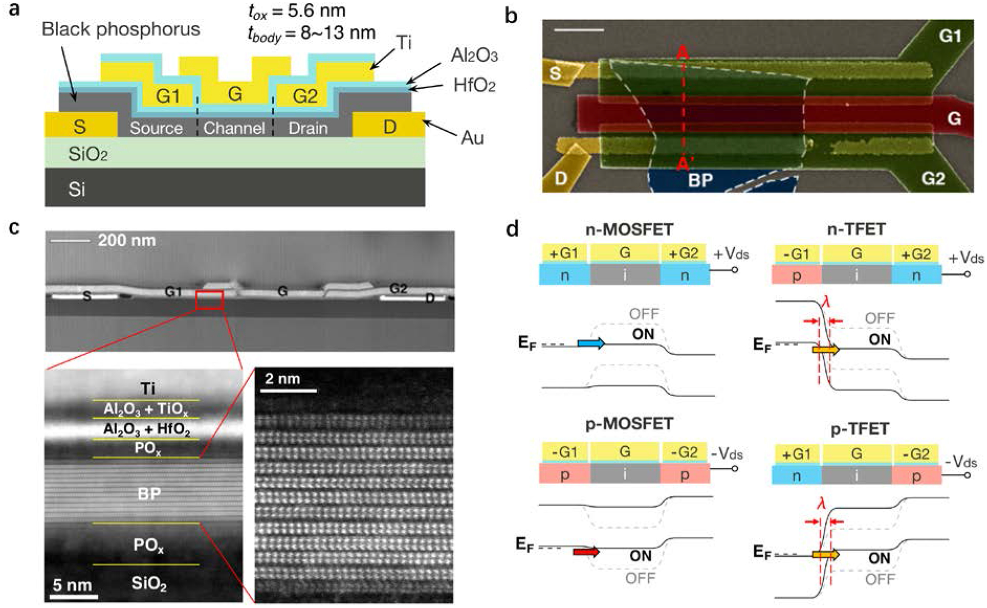
a, Schematic of the BP RED-TFET. b, Representative false-colored SEM image of the BP RED-TFET. Scale bar: 1 μm. c, Representative cross-section HAADF-STEM image of the BP RED-TFET along A-A’ in b, showing the triple top-gate structure, the interface of BP and gate oxide, and crystal structure of BP. d, Schematic illustration of the bands through the BP channel when reconfiguring the RED-TFET in the four operation modes, enabled by electrostatic doping as controlled by Vg1 and Vg2.
Depending on the operation mode, the device is characterized by different carrier injection mechanisms. As shown in Figure 1d, in the n-type (or p-type) MOSFET mode, by applying a positive (or negative) gate bias VG to the middle gate G, the bands in the “i” channel region are moved downwards (or upwards) to allow electrons (or holes) to be thermally injected from the source into the channel, turning the device from OFF to ON. On the other hand, in the n-type (or p-type) TFET mode, applying a positive (or negative) VG opens up a band-to-band tunneling window at the source-to-channel junction (Figure 1d), turning the device from OFF to ON. In the TFET modes, a thin gate dielectric thickness (tox) and a thin body thickness (tbody) together enable ideal electrostatics and ensure the abruptness of the tunneling junction through a small λ-value, which is essential to achieving steep subthreshold slopes and high tunneling currents.
Figure 2a shows the transfer (Ids − Vg) characteristics of a BP RED-TFET as a function of Vg1 in n-type configuration, i.e. for positive Vds and Vg2 (Vds = 0.8 V, Vg2 = 0.8 V). To illustrate the reconfigurability of our devices, first, a positive bias is applied to G1 (Vg1 = 1.1 V), resulting in an effective n-doping of both, the source and the drain region – the device thus exhibits an n/i/n doping profile across the BP flake – and operates in the n-type MOSFET mode. When Vg1 decreases progressively until Vg1 = −0.3 V, the n-doping level in the source region becomes lower and electron injection from the source metal contact into the source region is gradually suppressed, as shown in the band diagram in Figure 2b, resulting in steadily decreasing current levels as indicated by the solid black arrow in Figure 2a.
Figure 2 |. Transfer characteristics and reconfiguration of the BP RED-TFET.
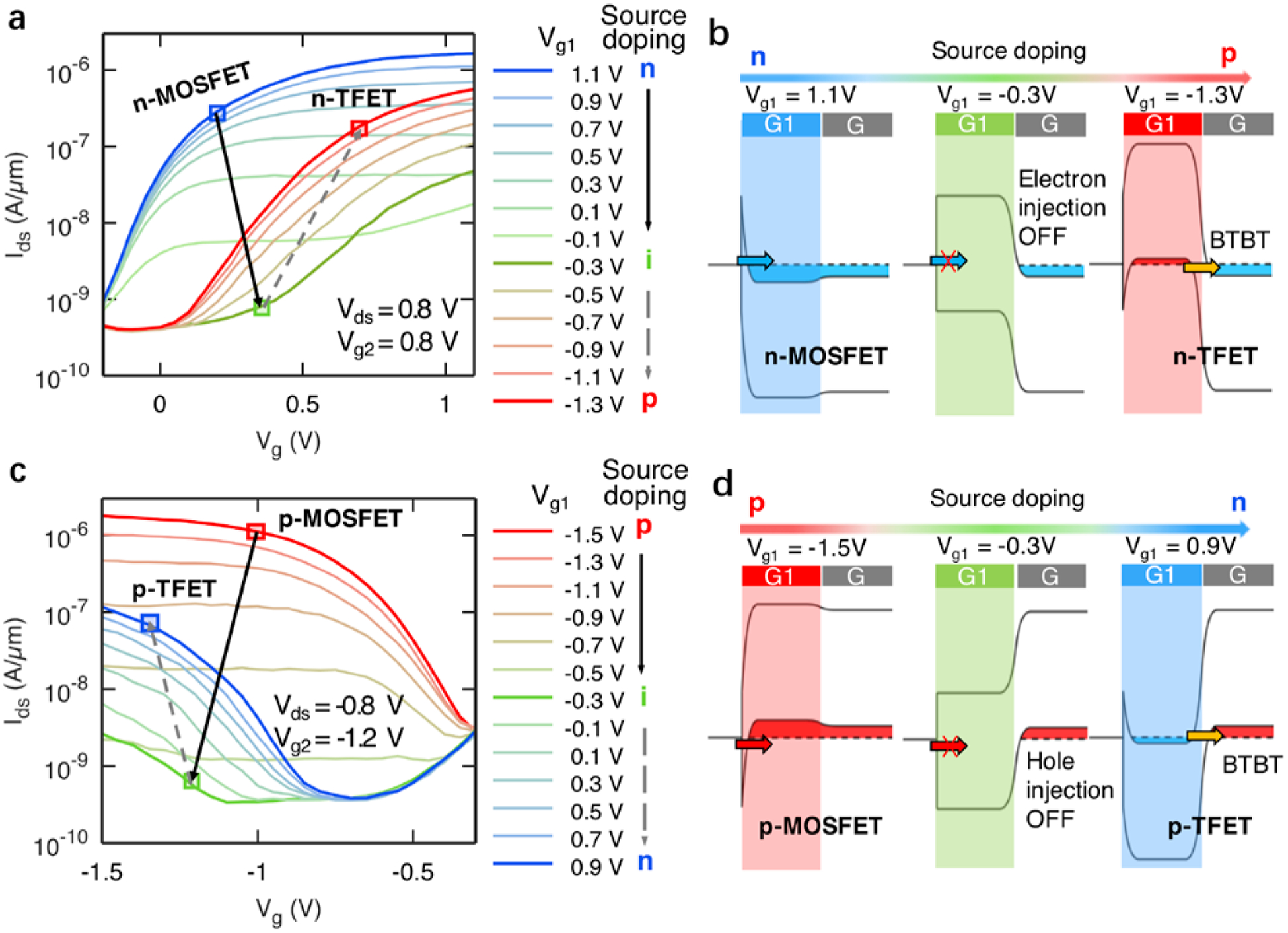
a, c, Transfer characteristics of the BP RED-TFET in (a) n-type and (c) p-type configurations under different source doping conditions, showing the transition from the MOSFET mode to the TFET mode. b, d, Band diagrams of the RED-TFET in (b) n-type and (d) p-type configurations corresponding to different source doping conditions in a, c respectively.
Next, when the G1 voltage is further decreased beyond Vg1 = −0.3 V, the doping in the source region becomes p-type. Under these conditions, current level start increasing again, indicated by the dashed gray arrow in Figure 2a. This at a first glance surprising non-monotonic trend occurs, since when the source doping is made effectively p-type, the device changes from a conventional n-type MOSFET with an n/i/n doping profile to an n-type TFET with a p/i/n doping profile and a BTBT window at the source-to-channel junction is opened, as shown in Figure 2b. As Vg1 is further decreased, the source region becomes even more substantially p-doped, and the BTBT window is enlarged, resulting in further increased current levels, as illustrated by the dashed gray arrow in Figure 2a. This non-monotonic trend of current level change with Vg1, or equivalently source doping level, is an unambiguous evidence for our claim of BTB tunneling in the device. Moreover, reconfigurable operation of our BP RED-TFET from the MOSFET mode to the TFET mode by tuning the source doping is demonstrated in this way for the first time. Similarly, transfer characteristics of a BP RED-TFET as a function of Vg1 in p-type configuration, i.e. for negative Vds and Vg2 (Vds = −0.8 V, Vg2 = −1.2 V) are shown in Figure 2c. When the source doping is changed from p-type to n-type by sweeping the G1 bias from Vg1 = −1.5 V to Vg1 = 0.9 V, one observes a similar non-monotonic trend of current level change as in Figure 2a and reconfiguration from the p-type MOSFET mode to the p-type TFET mode. The band diagrams of our BP RED-TFET changing from the p-type MOSFET mode to the p-type TFET mode are shown in Figure 2d.
The output characteristics (Ids - Vds) of the BP RED-TFET configured in (a) the p-type and n-type MOSFET mode and (b) the p-type and n-type TFET mode are displayed in Figure 3. Output saturation is observed for all four operation modes, indicating a good electrostatic control of the channel by the gate. Note that in the TFET modes, Ids increases nonlinearly with Vds for small Vds (Figure 3b). While nonlinear output characteristics are often seen as a sign for Schottky-barrier contacts, this explanation does not apply in our case. In fact, if the non-linearity would indeed be caused by the contacts, the device operating in the MOSFET modes with the same source doping configurations would also exhibit non-linearity in the output characteristics, which is clearly not the case in Figure 3a. Instead, the observed nonlinear increase in Ids originates from drain-induced-barrier-thinning (DIBT) of the BTBT barrier4, which is a consequence of the relatively large quantum capacitance of the black phosphorus channel. Therefore, it is exclusive to TFETs and not observed in MOSFETs where BTB tunneling barriers are absent. DIBT can be suppressed in the quantum capacitance limit31 and linear output characteristics can be recovered4. Transfer characteristics of the BP RED-TFET in n-type configuration under different temperatures are shown in Figure 4a. It is apparent that lowering the temperature results in reduced OFF current levels, due to suppressed thermionic injection from the drain (see inset of Figure 4a). Figure 4b shows a comparison of temperature-dependent Ids - Vg characteristics for a device operating in the n-type MOSFET mode and in the n-type TFET mode. The device shows distinctly different temperature-dependences when operating in these two modes due to different injection mechanisms. In the MOSFET mode, the carriers are thermally injected into the channel, therefore Ids - Vg has a strong dependence on temperature. By contrast, the carrier injection mechanism is BTB tunneling in the TFET mode, and Ids - Vg displays a much weaker dependence on temperature1, as shown in Figure 4b. Note that the increasing minimum OFF current with temperature in case of the TFET is due to an increase in thermionic injection at higher temperatures over the drain barrier biased at positive Vg2-values. Figure 4c compares SS-values versus temperature for the same device operating in the MOSFET mode and in the TFET mode. SS-values are extracted at a constant current of 5 nA, in order to avoid the impact of the temperature-dependent thermionic current cut-off (dashed orange lines in Figure 4a) on the SS-extraction. As expected, SS-values increase with temperature in case of the MOSFET mode while remaining constant in the TFET mode. Also note that the minimum SS-value at room temperature for band-to-band tunneling is 178 mV/dec, well above 60 mV/dec. This is in part due to the choices of flake thickness and gate dielectrics as discussed below but also related to the fact that the steepest slopes in case of TFETs occur at the lowest current levels. In fact, when analyzing the green curve at Vg1=−0.1V at 100K, an SS-value of 84 mV/dec is extracted. Note that BTBT is largely temperature independent and that this number would have thus been expected also at 300K, if the same minimum OFF-current would have been achievable.
Figure 3 |. Output characteristics of the BP RED-TFET.
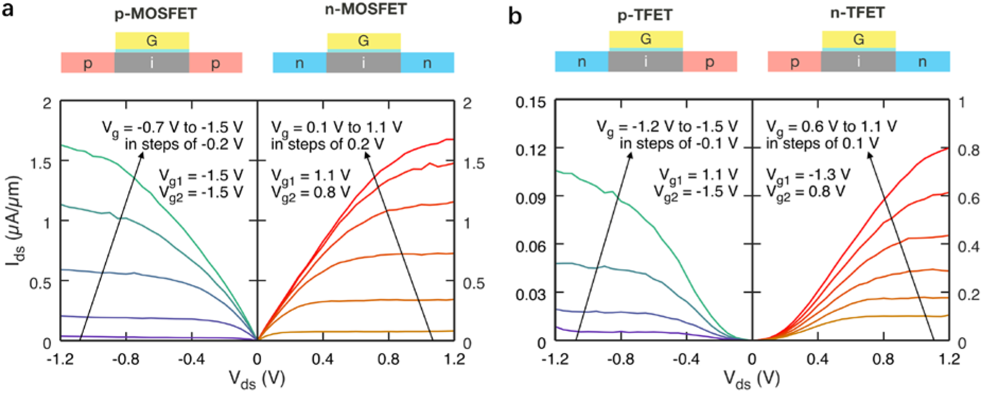
a, Output characteristics of the BP RED-TFET in the p-type and n-type MOSFET mode. The saturation behavior indicates a good gate control on the channel. b, Output characteristics of the BP RED-TFET in the p-type and n-type TFET mode. Non-linear output onsets are observed due to drain-induced-barrier thinning (DIBT) effect.
Figure 4 |. Temperature-dependent measurements.
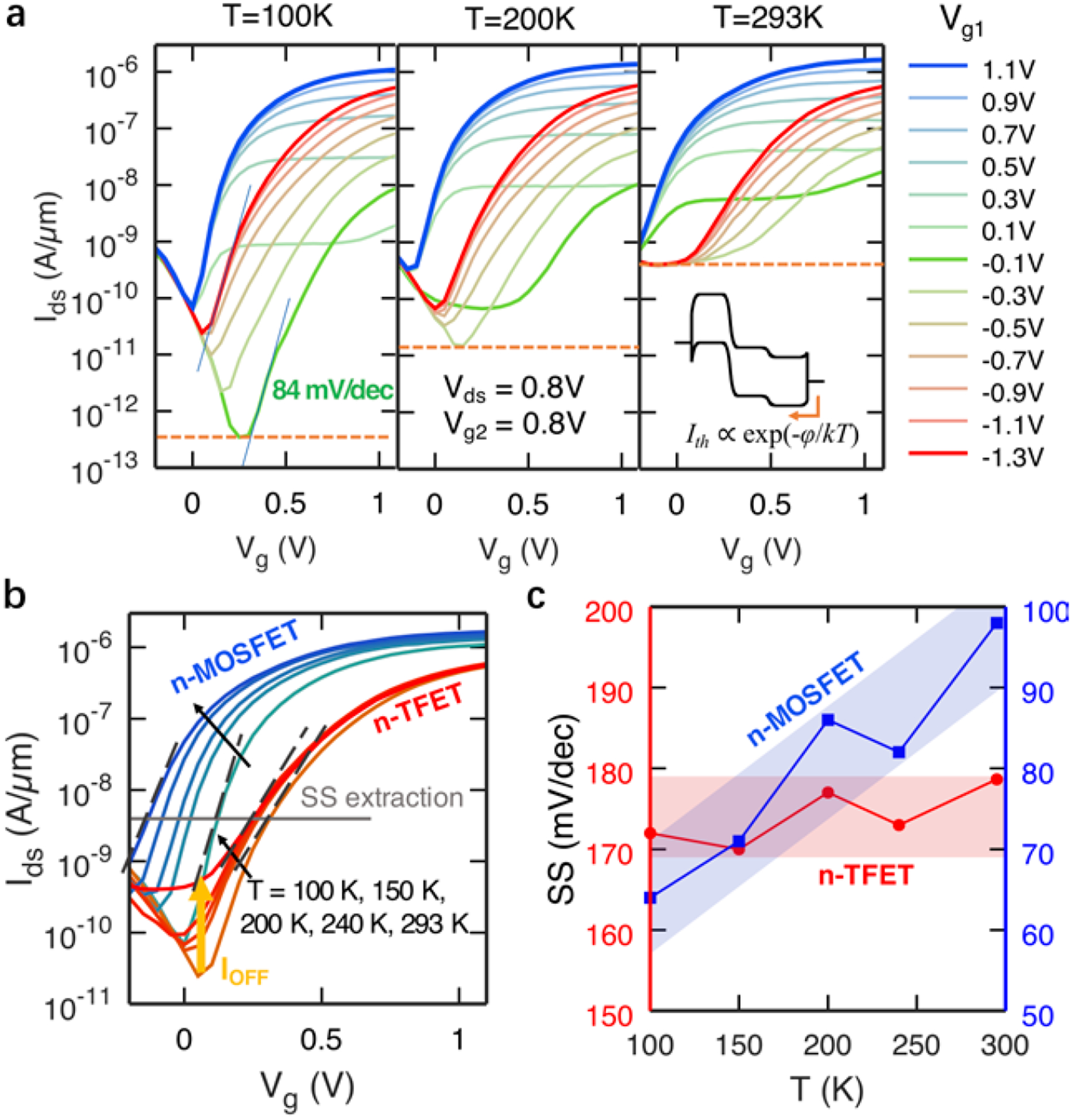
a, Comparison of transfer characteristics of the BP RED-TFET at 100K, 200K and 293K, showing increasing OFF-current levels at elevated temperatures. Dashed orange lines indicate thermionic current cut-off limits. The inset shows a band diagram explaining the impact of thermionic injection from the drain at higher temperatures. b, Comparison of transfer characteristics of the BP RED-TFET in the n-type MOSFET mode and the n-type TFET mode at different temperatures. In the n-TFET mode, the transfer characteristics show a weaker temperature dependence compared with the operation in the n-MOSFET mode, except for a rise in the minimum OFF current level due to thermal injection. c, Comparison of experimental subthreshold swing (SS) values versus temperature for the BP RED-TFET operating in the n-type MOSFET mode and the n-type TFET mode.
In order to boost the performance of BP TFETs further, channel body and oxide thicknesses need to be aggressively scaled down20. As one can see from equation (1), the performance of a TFET not only depends on material parameters such as Eg and m*, but in particular also on the screening length λ, which in turn depends on tox and tbody. In order to make quantitative projections about the potential performance improvement of 2D BP TFETs with scaled down tox and tbody, self-consistent atomistic simulations are first performed using NEMO5 toolsets32,33 to match the experimental data obtained in this study. Figure 5a shows a comparison of simulated Ids − Vg and measured TFET characteristics, showing good agreement between simulation and experimental data. Note that to achieve this matching we made use of our findings from Figure 1c. To describe the experimental results (Exp. 1) for a device with a nominal thickness of tbody=8.3 nm and tox=5.6 nm properly, t’body=3 nm and a t’ox=7.5 nm were assumed in the simulations to account for formation of the above mentioned POx layers (see Supplementary Section 1). Under these assumptions, both, the inverse subthreshold slope as well as the actual current levels are properly reproduced (see Figure 5a). Moreover, when performing a similar comparison for a device from a slightly thicker BP flake, a t’body=7 nm and a t’ox=8.1 nm in the simulation nicely match the experimental results for the nominal values of tbody=12.8 nm and a tox=6.2 nm (Exp. 2 in Figure 5a). All simulations are performed with transport direction along the armchair direction of BP (see Supplementary Section 6). With this calibration in place, we are in a position to carry out projections based on simulations for aggressively scaled BP TFETs. Figure 5b shows simulated Ids − Vg of a BP TFET when scaling down the oxide to an EOT = 0.5 nm while keeping the same channel thickness of t’body=3 nm and etching the spacers between separate gates to achieve better electrostatic conditions34 (black line). This approach results in significant improvements in the steepness of the subthreshold region and ON-current levels. Moreover, further scaling down the channel thickness to a single mono-layer (blue line) results in ION = 800 μA/μm and SS = 12 mV/dec values, clearly highlighting the potential of BP TFETs in future applications.
Figure 5 |. Projections for BP TFET performance.
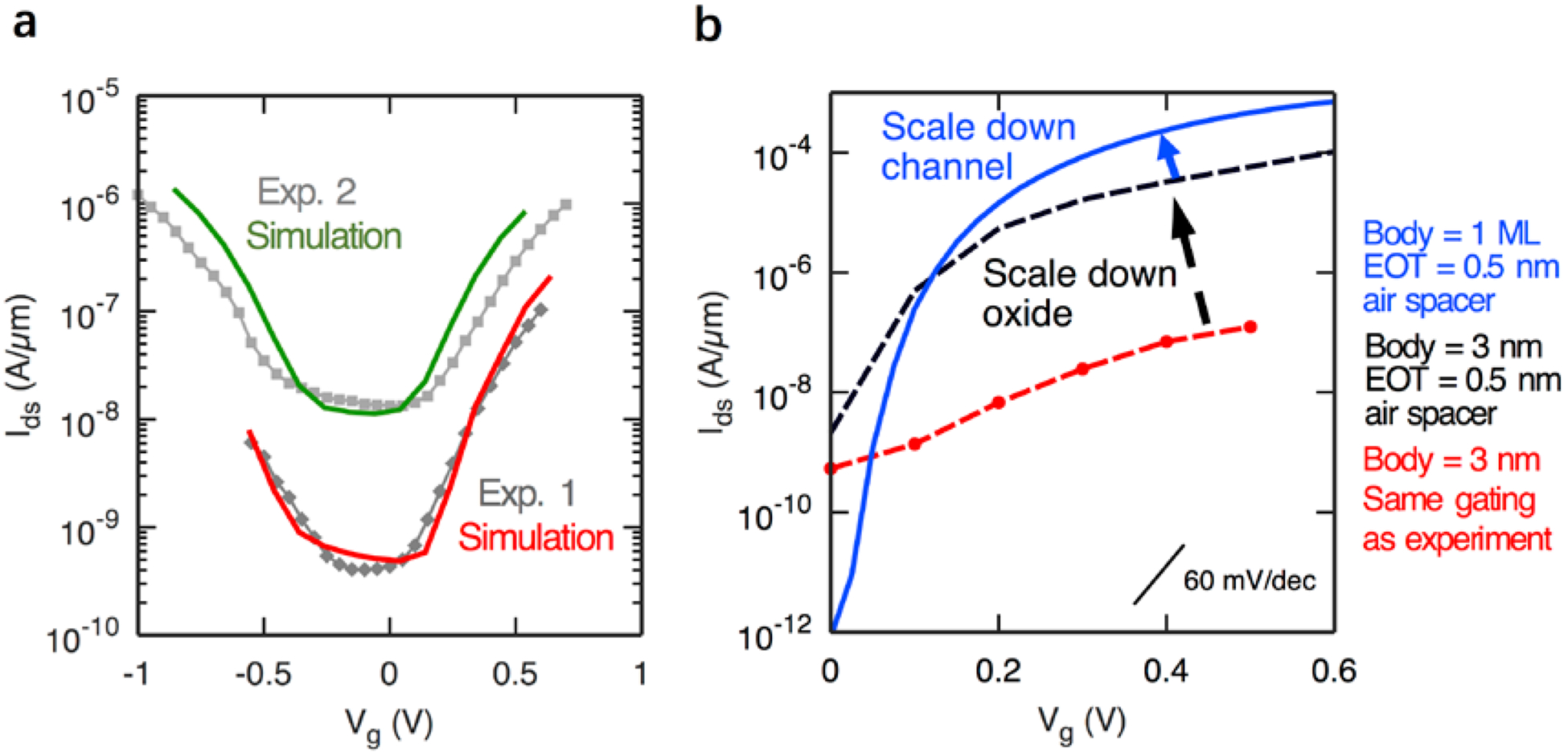
a, Atomistic simulations, solid lines, of Ids - Vg for the BP TFET, showing good agreement with experimental data (gray dots). Exp. 1 refers to measurements performed on a device as shown in Figure 1 with a nominal 8.3 nm body and with gate G1 and G2 having configurations (−1.3 V, 0.8 V). The simulation has been performed with a smaller BP thickness of 3 nm and a thicker oxide to account for the oxidation (see Supplementary Section 1). Exp. 2 is a measurement of an earlier prototype device with a thicker BP flake of 12.8 nm that has been simulated with 7 nm to account for the oxidation. b, Simulation of the fabricated BP TFET shown in blue. Improving the electrostatics by using HfO2 with an EOT = 0.5 nm and etching the spacer is expected to significantly improve steepness and current levels as shown in black. Further improvements can be achieved by scaling down the channel into a mono-layer (ML) BP as shown in blue.
In conclusion, we have demonstrated reconfigurable BP TFETs. The TFETs exhibit ON-currents of up to 0.6 μA/μm and subthreshold swings of 170 mV/dec at room temperature for Vds = 0.8 V. The device can be reconfigured to behave as an n/p-type TFET and as an n/p-type MOSFET owing to electrostatic doping control of three separate top gates. Atomistic simulations predict that the performance of BP TFETs can be further improved towards ION = 800 μA/μm and SS = 12 mV/dec with scaled down channel and oxide thicknesses. Our BP RED-TFET provides a guide for energy-efficient tunneling devices based on 2D materials.
Methods
Device fabrication and electrical characterization
Ti/Au (10 nm/20 nm) contacts were deposited onto a silicon substrate with 90 nm of silicon dioxide (SiO2) on top and patterned using e-beam lithography and lift-off process. BP flakes were exfoliated onto the Au contacts from bulk crystals using mechanical exfoliation. A thin layer of Al was e-beam evaporated on top of BP, which formed a 1.3 nm thick aluminum oxide upon exposure to air and acted as seeding layer for the subsequent ALD process. A bilayer dielectric stack composed of 0.8 nm of HfO2 and 2.2 nm of Al2O3 was deposited by a thermal ALD process at 200 °C to form gate dielectrics for G1 and G2. Next, G1 and G2 were defined by subsequent e-beam lithography and e-beam evaporation of 40 nm Ti. The sample is annealed in forming gas for 3 hrs at 300 °C to improve the quality of the gate dielectric. To achieve proper isolation between gates G1/G2 and G, while maintaining relatively thin dielectric thicknesses for gate G, the Al2O3 between the G1 and G2 regions was removed by wet etching, with G1 and G2 metals as masks and HfO2 as etch stop layer. A second ALD process was performed to deposit another 3.5 nm Al2O3 layer as gate dielectric for G, as well as to ensure isolation between G1/G2 and G. The total oxide thickness for gate G is 5.6 nm. The device fabrication is finalized by depositing 40 nm Ti to form gate G. Room-temperature and low-temperature electrical characterization of the device was performed in a LakeShore FWPX Cryogenic Probe Station at a vacuum level below 10−5 Torr using an Agilent 4156C Parameter Analyzer.
Atomistic simulation
The atomistic quantum transport simulation results have been obtained from a self-consistent solution of the 3D-Poisson equation and by employing the Non-Equilibrium Green’s Functions (NEGF) method using the Nanoelectronics modeling tool NEMO532,33. The Poisson equation provides the potential for the NEGF method and takes the free charge in return. The tight-binding Hamiltonian of phosphorene used in NEGF calculations employs a 10 bands sp3d5s* 2nd nearest neighbor model. More details on the Poisson equation with anisotropic dielectric tensor and NEGF equations can be found in our previous works8,9.
Transmission electron microscopy (TEM) characterization
An FEI Nova NanoLab 600 DualBeam (SEM/FIB) was employed to prepare cross-sectional TEM samples. Carbon was deposited on top of the device to protect the surface. To reduce Ga-ions damage, in the final step of preparation the TEM samples were thinned with 2 kV Ga-ions using a low beam current of 29 pA and a zero-degree incident angle. An FEI Titan 80–300 probe-corrected scanning transmission electron microscope (STEM) equipped with monochromator and GIF Tridiem electron energy loss spectrometer (EELS) system was employed to acquire atomic-resolution high-angle annular dark field (HAADF) images and EELS based spectrum-images. HAADF images were acquired with the detector semi-angular collection range of 35 – 195 mrad. The spectrum-images were acquired with a condenser aperture convergence semi-angle of 13 mrad and a spectrometer entrance aperture collection semi-angle of 14 mrad.
Supplementary Material
Acknowledgements
This work was supported in part by the Center for Low Energy Systems Technology (LEAST), one of the six SRC STARnet Centers, sponsored by MARCO and DARPA. This work used the Extreme Science and Engineering Discovery Environment (XSEDE)35, which is supported by National Science Foundation grant number ACI-1548562. nanoHUB.org computational resources were used for the atomistic simulations. Operated by the Network for Computational Nanotechnology funded by the US National Science Foundation under grants EEC-1227110, EEC-0228390, EEC-0634750, OCI-0438246, and OCI-0721680. H. Z. acknowledges support from the U.S. Department of Commerce, National Institute of Standards and Technology under the financial assistance awards 70NANB15H025 and 70NANB17H249. A. V. D. acknowledges the support of Material Genome Initiative funding allocated to NIST. Disclaimer: certain commercial equipment, instruments, or materials are identified in this paper in order to specify the experimental procedure adequately. Such identification is not intended to imply recommendation or endorsement by the National Institute of Standards and Technology.
Footnotes
Competing financial interests.
The authors declare no competing financial interests.
References:
- 1.Appenzeller J, Lin Y-M, Knoch J & Avouris P, Band-to-band tunneling in carbon nanotube field-effect transistors. Phys. Rev. Lett 93, 196805 (2004). [DOI] [PubMed] [Google Scholar]
- 2.Appenzeller J et al. , Comparing carbon nanotube transistors-the ideal choice: a novel tunneling device design. IEEE Trans. Electron Devices 52, 2568–2576 (2005). [Google Scholar]
- 3.Ionescu AM & Riel H, Tunnel field-effect transistors as energy-efficient electronic switches. Nature 479, 329 (2011). [DOI] [PubMed] [Google Scholar]
- 4.Knoch J & Appenzeller J, Tunneling phenomena in carbon nanotube field-effect transistors. physica status solidi (a) 205, 679–694 (2008). [Google Scholar]
- 5.Memisevic E, Svensson J, Hellenbrand M, Lind E & Wernersson L-E, Vertical InAs/GaAsSb/GaSb tunneling field-effect transistor on Si with S = 48 mV/decade and Ion = 10 μA/μm for Ioff = 1 nA/μm at Vds = 0.3 V, in IEEE Int. Electron Devices Meet. (IEEE, 2016). [Google Scholar]
- 6.Sarkar D et al. , A subthermionic tunnel field-effect transistor with an atomically thin channel. Nature 526, 91 (2015). [DOI] [PubMed] [Google Scholar]
- 7.Seabaugh AC & Zhang Q, Low-voltage tunnel transistors for beyond CMOS logic. Proc. IEEE 98, 2095–2110 (2010). [Google Scholar]
- 8.Ameen TA, Ilatikhameneh H, Klimeck G & Rahman R, Few-layer phosphorene: An ideal 2D material for tunnel transistors. Sci. Rep 6, 28515 (2016). [DOI] [PMC free article] [PubMed] [Google Scholar]
- 9.Ilatikhameneh H, et al. Saving Moore’s law down to 1 nm channels with anisotropic effective mass. Sci. Rep 6, 31501 (2016). [DOI] [PMC free article] [PubMed] [Google Scholar]
- 10.Radisavljevic B, Radenovic A, Brivio J, Giacometti i. V. & Kis A, Single-layer MoS2 transistors. Nature Nanotech. 6, 147–150 (2011). [DOI] [PubMed] [Google Scholar]
- 11.Das S & Appenzeller J, WSe2 field effect transistors with enhanced ambipolar characteristics. Appl. Phys. Lett 103, 103501 (2013). [Google Scholar]
- 12.Li L et al. , Black phosphorus field-effect transistors. Nature Nanotech. 9, 372–377 (2014). [DOI] [PubMed] [Google Scholar]
- 13.Liu H et al. , Phosphorene: An Unexplored 2D Semiconductor with a High Hole Mobility. ACS Nano 8, 4033–4041 (2014). [DOI] [PubMed] [Google Scholar]
- 14.Das S, Chen H-Y, Penumatcha AV & Appenzeller J, High performance multilayer MoS2 transistors with scandium contacts. Nano Lett. 13, 100–105 (2013). [DOI] [PubMed] [Google Scholar]
- 15.Penumatcha AV, Salazar RB & Appenzeller J, Analysing black phosphorus transistors using an analytic Schottky barrier MOSFET model. Nature Commun. 6 (2015). [DOI] [PMC free article] [PubMed] [Google Scholar]
- 16.Wang H et al. , Integrated circuits based on bilayer MoS2 transistors, Nano Lett. 12, 4674–4680 (2012) [DOI] [PubMed] [Google Scholar]
- 17.Choi Y-K et al. , Ultra-thin body SOI MOSFET for deep-sub-tenth micron era, in IEEE Int. Electron Devices Meet. (IEEE, 1999) [Google Scholar]
- 18.Skotnicki T, Hutchby JA, King T-J, Wong H-S & Boeuf F, The end of CMOS scaling: toward the introduction of new materials and structural changes to improve MOSFET performance. IEEE Circuits and Devices Magazine 21, 16–26 (2005) [Google Scholar]
- 19.Das S, Prakash A, Salazar R & Appenzeller J, Toward low-power electronics: tunneling phenomena in transition metal dichalcogenides. ACS Nano 8, 1681–1689 (2014). [DOI] [PubMed] [Google Scholar]
- 20.Ilatikhameneh H et al. , Tunnel field-effect transistors in 2-D transition metal dichalcogenide materials. IEEE J. Explor. Solid-State Computat. Devices Circuits 1, 12–18 (2015). [Google Scholar]
- 21.Ilatikhameneh H, Salazar RB, Klimeck G, Rahman R & Appenzeller J, From Fowler--Nordheim to nonequilibrium Green’s function modeling of tunneling. IEEE Trans. Electron Devices 63, 2871–2878 (2016). [Google Scholar]
- 22.Yan R et al. , Esaki diodes in van der Waals heterojunctions with broken-gap energy band alignment. Nano Lett. 15, 5791–5798 (2015). [DOI] [PubMed] [Google Scholar]
- 23.Li MO, Yan R, Jena D & Xing HG, Two-dimensional heterojunction interlayer tunnel FET (Thin-TFET): From theory to applications, in IEEE Int. Electron Devices Meet . (IEEE, 2016). [Google Scholar]
- 24.Müller MR et al. , Gate-Controlled WSe2 Transistors Using a Buried Triple-Gate Structure. Nanoscale Research Lett. 11, 512 (2016). [DOI] [PMC free article] [PubMed] [Google Scholar]
- 25.Seabaugh A et al. , Steep subthreshold swing tunnel FETs: GaN/InN/GaN and transition metal dichalcogenide channels, IEEE Int. Electron Devices Meet . (IEEE, 2015). [Google Scholar]
- 26.Sze SM & Ng KK, Physics of Semiconductor Devices (John wiley & sons, 2006). [Google Scholar]
- 27.Knoch J, Mantl S & Appenzeller J, Impact of the dimensionality on the performance of tunneling FETs: Bulk versus one-dimensional devices. Solid-State Electronics 51, 572–578 (2007). [Google Scholar]
- 28.Prakash A & Appenzeller J, Bandgap Extraction and Device Analysis of Ionic Liquid Gated WSe2 Schottky Barrier Transistors. ACS Nano 11, 1626–1632 (2017). [DOI] [PubMed] [Google Scholar]
- 29.Qiao J, Kong X, Hu Z-X, Yang F & Ji W, High-mobility transport anisotropy and linear dichroism in few-layer black phosphorus. Nature Commun. 5 (2014). [DOI] [PMC free article] [PubMed] [Google Scholar]
- 30.Wu P, Prakash A & Appenzeller J, First Demonstration of Band-to-Band Tunneling in Black Phosphorus, in 75th Device Research Conference (2017) [Google Scholar]
- 31.Knoch J, Reiss W & Appenzeller J, Outperforming the conventional scaling rules in the quantum-capacitance limit. IEEE Electron Device Lett. 29, 372–374 (2008). [Google Scholar]
- 32.Steiger S, Povolotskyi M, Park H-H, Kubis T & Klimeck G, NEMO5: A Parallel Multiscale Nanoelectronics Modeling Tool. IEEE Trans. Nanotech 10, 1464–1474 (2011). [Google Scholar]
- 33.Fonseca JE et al. , Efficient and realistic device modeling from atomic detail to the nanoscale. J. Comput. Electron 12, 592–600 (2013). [Google Scholar]
- 34.Ilatikhameneh H, et al. , Dielectric engineered tunnel field-effect transistor. IEEE Electron Device Lett. 3, 1097–1100 (2015). [Google Scholar]
- 35.Towns J et al. , XSEDE: Accelerating Scientific Discovery. Computing in Science & Engineering. 16, 62–74 (2014) [Google Scholar]
Associated Data
This section collects any data citations, data availability statements, or supplementary materials included in this article.