Abstract
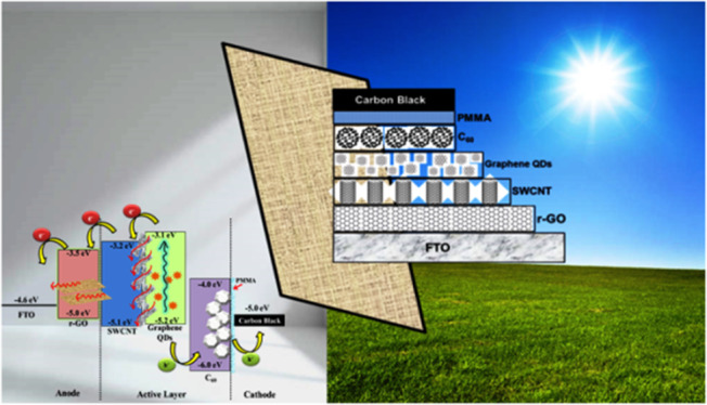
The self-assembling characteristics allow carbon nanomaterials to be readily explored, environmentally benign, solution-processed, low-cost, and efficient solar light-harvesting materials. An effort has been made to replace the regular photovoltaic device’s electrodes by different carbon allotrope-based electrodes. Sequential fabrication of carbon solar cells (SCs) was performed under ambient conditions, where FTO/graphene/single-walled carbon nanotubes/graphene quantum dots-fullerene/carbon black paste layers were assembled with poly(methyl methacrylate) (PMMA) as an encapsulating layer. The PMMA layer provides significant improvement toward the entry of water vapor, hence leading to stability up to 1000 h. The photoconversion efficiency of the PMMA-encapsulated carbon SC has been increased by ∼105% and the stability decreased by only ∼10% after 1000 h of exposure to environmental moisture. Besides, the building integrated photovoltaic window properties achieved using this carbon SC were also investigated by using the color rendering index and the correlated color temperature, which can have an impact on the buildings’ occupants’ comfort. This study leads to an extensive integration to improve carbon-based materials because of their effective and useful but less-explored characteristics suitable for potential photovoltaic applications.
1. Introduction
To meet our energy demands, solar energy stands out as the most viable choice among all the other renewable energy options.1,2 To obtain the best solution for this, new solar-to-electric power conversion strategies are under development. New nanostructured material designing for next-generation solar cell (SC) development has been an extensive area of research. Photovoltaic (PV) SCs made of organic compounds would offer a variety of advantages over the traditional SCs in terms of their low-cost and simpler manufacturing. Recently, carbon has gained considerable attention because of its cost-effectiveness, environmental superiority, abundancy, and excellent photoelectrochemical catalytic activity toward the redox species. A wide variety of insulator (diamond) to metallic/semimetallic (graphite) and conducting/semiconducting (fullerenes and carbon nanotubes) compounds that have distinct chemical, electronic, and physical properties similar to carbon can be arranged to produce carbon-based devices.3,4 In addition, collective implementation of all-carbon materials could create novel optoelectronic properties. Carbon-based structures were already established as a superior candidate for the modern field of renewable energy (such as photovoltaics, photoelectrochemical devices, energy storage, and so forth) and environmental science (water purification, desalination, waste treatment, etc.).5,6 At the same time, these materials can be treated readily using solution processes. Owing to its unique structure and physicochemical properties, various forms of carbon generate a great deal of interest in energy conversion and storage.7−10 Inclusion of different carbon materials in PV cells, especially in organic SCs, dye-sensitized SCs (DSSCs), and perovskite SCs (PSCs) is widely studied in the popular PV research field. With the extensive study on graphene-based materials, it has been realized that the fast electron transfer is essential for good optoelectronic properties to solve many concerns that are common in DSSC- and PSC-related research.11−13 The carbon allotropes are directly assembled as a layered structure in the form of films or fibers obtained by colloidal synthesis and fabrication methods. All these features make carbon-based devices a potential candidate for next-generation electronics. Fullerenes were first reported as an excellent material for SC fabrication by Koltun et al. (1996).14 After that, not much research has been conducted using carbon-based materials for the PV sector. Later on, Ramuz et al. (2012) reported the all-carbon SC fabrication.15 Similarly, Lee et al. (2012) described an all-carbon counter electrode for DSSCs.16 An efficient way to develop fiber-shaped DSSCs based on an all-carbon electrode was reported by Cai et al. (2012).17 However, the stability of these cells is yet to be studied for practical implementation. Compared to traditional DSSCs and PSCs, graphene photoanodes have indeed demonstrated improved performance. Therefore, it is anticipated that a combination of single-walled carbon nanotubes (SWCNTs), which possess efficient carrier transport ability, and graphene oxide (GO) having the electron blocking ability should function as an efficient carrier transport layer.18 Besides, because of higher photon absorption and faster charge extraction, graphene quantum dots (GQDs) may behave like a sensitizer.19 Fullerene-C60 acts as a good hole-transporting material in the case of organic SCs or PSCs.20 Therefore, the combination of all these carbon materials and their synergistic effect can potentially lower the cost of traditional photovoltaic cells. However, it is difficult to proceed with solution-based carbon materials because of limited solvent availability that can disperse or dissolve graphitic nanostructures, and accordingly they are required to modify their surfaces with various polymeric or surfactant-induced processes. The mechanisms for different allotropes of carbon in photovoltaic applications are yet to be completely perceived and require necessary justification for further investigation toward the use of carbon-based DSSCs and PSCs. The main barrier for the commercial use of these SCs is the poor device stability. For carbon-based SCs, device instability from photodegradation is an issue, which needs to be rectified. Encapsulation by employing a material or layer that require against oxygen and moisture has been recognized as one of the holistic approaches to address this instability issue and enhance the device stability.21 Polymethyl methacrylate (PMMA) has the ability to protect the core active layer of the cell from oxygen and moisture by forming a compact layer using cross-linked carbon nanomaterials.22−26 This cost-effective, nonhazardous polymer layer contributes to improved photoconversion efficiency (PCE) as well as stability to the device. The PV technology integrated into buildings is another novel approach, where PV devices replace the traditional building envelopes (the window, roof, and wall). Introduction of PV into buildings not only generates power but also controls the transmitted light into the building interior. Thus, semitransparent nature is the precondition for this type of PV cell.27 Herein, we report the facile preparation and emerging photovoltaic applications of different carbon allotropes, where the incorporated PMMA layer acts as an encapsulating layer for moisture to improve the device efficiency as well as stability. Integration of this cell technology in a building in the form of a building integrated photovoltaic (BIPV) window can concomitantly offer clean microenergy generation and occupant comfort. Along with the fundamental function of benign electricity generation, the BIPV also enhances the building envelope design and offers economic advantages, which in turn also reduce the environmental issues.28−30 Therefore, BIPV window properties realized using this carbon SC were also investigated.
2. Materials and Methods
2.1. Preparation of Carbon-Based SCs
Fabrication of carbon-based SC has been inspired by the literature.15 In detail, reduced GO (rGO) preparation involved the addition of 1 mL of hydrazine hydrate (Fisher Scientific) to a typical 10 mL of a commercial GO (2 mg/mL, dispersion in H2O, Sigma-Aldrich) solution in a glass vial. The solution was stirred continuously for 30 min at 70 °C to precipitate down completely, and the solution turned black. Next, the rGO solution was spin-coated at 1000 rpm for 1 min on an etched fluorine-doped tin oxide (FTO) glass (2.0 cm × 2.0 cm, 7 Ω/cm2). At 100 °C, the substrates were annealed by keeping it on a hot plate for 1 h. Ice water bath sonication was performed for 30 min with an aqueous solution of single-walled carbon nanotubes (SWCNTs) (Sigma-Aldrich) in N-methyl-2-pyrrolidone (Sigma-Aldrich). The solution was then centrifuged for 30 min at 10,000 rpm to remove any excess contamination or agglomeration of the SWCNT bundle. The decanted solution was spin-coated for 1 min at 1500 rpm on top of the rGO-coated FTO photoanode layer and dried at 100 °C for 30 min. Furthermore, 100 μL of GQDs (Sigma-Aldrich, 1 mg/mL in water) solution was spin-coated and air-dried. Next, commercially available Fullerene-C60 (sublimed, Sigma-Aldrich) was thermally deposited under vacuum (5 × 10⁵ Torr) at 0.05 nm/s. Poly(methyl methacrylate) or PMMA (40 mg/mL in chlorobenzene) was sequentially spin-coated on the C60 layer at a rotation speed of 4000 rpm for 30 s, followed by drying for 30 min at 70 °C. Similarly, on top of the PMMA layer, carbon paste (Solaronix, 45411) was evaporated under 5 × 10⁵ Torr vacuum pressure at 0.05 nm/s (using an evaporator from Thermionics Laboratory, Inc.). Figure 1a illustrates the sequential fabrication process of a solution-processed carbon SC.
Figure 1.
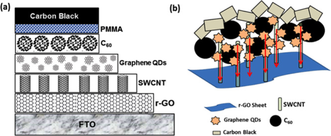
Schematic diagram of the (a) sequential fabrication of carbon SC using different allotropes of carbon and (b) probable arrangement of different allotropes used during the sequential fabrication of carbon SCs.
2.2. Material Characterization and Device Performance Evaluation
PV performances of this carbon-based SC device were explored by using an AAA standard continuous Wacom solar simulator (model no: WXS-210S-20) under 1000 W/m2 of light intensity and AM 1.5G illumination. An EKO MP-160i I–V tracer recorded the I–V data for the PV cells. The active area of the device was 0.16 cm2. An Autolab frequency analyzer equipped with an Autolab PGSTAT 10 measured the electrochemical impedance, while the same indoor solar simulator was employed with the frequency range between 0.1 and 100 kHz. All the devices were measured at their corresponding open circuit voltage. The device microstructural analysis and PMMA encapsulation imaging were done by field-emission scanning electron microscopy (FESEM) on a Tescan Vega3 equipped with an Oxford Instruments Elemental Analyzer. An Ossila contact angle goniometer recorded the water contact angle image of the device to understand the device stability under moist ambient conditions. A PerkinElmer Lambda 1050 UV/vis/NIR spectrophotometer measured the device transparency, where bare refers to blank FTO without any carbon coating. The infrared (IR) transmission before and after PMMA encapsulation was determined using an Fourier transform infrared (FTIR) spectroscopy setup (Bruker V80). The atomic force microscopy (AFM) studies were performed using a Bruker Innova AFM before and after PMMA encapsulation in the device.
The external quantum efficiency (EQE) of the carbon-based devices was recorded using a monochromatic light from 300 to 1100 nm using a Bentham PVE300 system. Theoretical short-circuit current density values were obtained by integrating the AM 1.5G solar spectrum with the product of the EQE spectrum and matching with the measured short circuit current density (JSC) to within the limit of 5%. The internal quantum efficiency (IQE) spectra were obtained by the division of the EQE by the reflectance of the device, as recorded using a Lambda 1050 UV/vis/NIR spectrophotometer from PerkinElmer.
2.3. Proposed Carbon-Based SC Architecture
The proposed idea of using different allotropes of carbon is schematically described in Figure 1b. Different carbon allotropes could generate improved ion conductance by shortening the ion pathway in terms of their morphology and band gap tuning. The layer formation was executed by the electrostatic interactions between the positively charged SWCNTs and the negatively charged nanosheets of rGO. Furthermore, the quenched emission of GQDs strongly indicates the successful attachment of SWCNTs.31 The carbon paste has been used as an effective substitute for costly noble metals featuring a similar work function like them.32 Therefore, the selected allotropes can be suitable for their size-tunable optical response and superiority of large optical absorptivity resulting in efficient multiple carrier generation. All carbon composites using a simpler solution process enable stacking of layers in a conventional configuration.
3. Results and Discussion
3.1. Microstructural and Optical Analyses
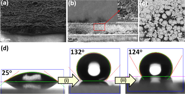
The microstructural investigation was performed by SEM before depositing the carbon black layer, as shown in Figure 2a–c. The SEM cross-sectional image of the carbon SC exhibited a rough surface, as shown in Figure 2a,b, and the average thickness of the overall cell was found to be ∼10 μm. Nearly uniform thickness was revealed for the electrodes from the microstructural analysis, which is influential to obtain a high photovoltaic efficiency. Figure 2c shows the top view microstructural image of the GQDs and the C60 assembled layer. Agglomeration of particles may have resulted in the formation of a sheet-like continuous layer of carbon materials.
Figure 2.
(a,b) Cross-sectional FESEM images of the carbon SC before addition of the carbon paste layer, (c) top-view FESEM image of GQDs and the fullerene layer of the carbon SC, and (d) WCA measurement digital images of the carbon-based devices with and without PMMA.
Using hydrophobic hole-transport layers (HTLs) can serve as one of the most promising approaches.33 Mostly, the HTL rests between the absorber layer and the top electrodes, which can act as a secondary vapor retardation layer that prohibits moisture from reaching the absorber layer. PMMA has the ability to create an intercross-linked network-based compact layer to provide protection from oxygen and moisture, improve the air stability, and give mechanical strength. As a result, restriction of oxygen and moisture inside the device passivates a smooth electron flow and delivers an improved lifetime. The result of moisture protection has been recorded using water contact angle (WCA) measurements. The as-prepared carbon SC exhibits hydrophobic nature, which shows the WCA value of ∼25°. After depositing the PMMA layer, the WCA value tremendously increased to 132° (step i), and after 1000 min, there is a minor decrement of the WCA value to 124° (step ii). This result clarifies the importance of the PMMA layers in vapor protection.
3.2. PV Performance
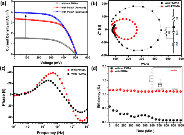
An evaluation of the photovoltaic performances of the fabricated carbon-based devices was done under 1 sun 1.5 AM. The performances of the current density versus voltage (J–V) characteristic plot of the carbon devices with and without PMMA are shown in Figure 3a to understand the effect of PMMA on the photovoltaic performance. The PMMA-based carbon device exhibited a maximum PCE of 1.15% with a short circuit current density (JSC) of 3.93 mA/cm2, an open circuit voltage (VOC) 0.60 V, and a fill factor (FF) of 0.61. On the contrary, without PMMA-based carbon devices exhibited a PCE of 0.31%, with a JSC of 2.89 mA/cm2, a VOC of 0.56 V, and an FF of 0.56. The recorded J–V characteristic parameters are further compared in Table 1. As a result, using the PMMA layer, the corresponding device exhibits ∼105% higher efficiency than the device without a PMMA layer. This outcome is quite competitive than the previously published PMMA-incorporated SC. Electrochemical impedance analysis was performed through Nyquist and Bode plots under 1000 W/m2 illumination and a bias of 0.6 V for both the devices, as shown in Figure 3a,b, respectively. Similar interfacial charge transfer processes can be seen for both the devices, as obtained from the results. The Nyquist plots (Figure 3a) derived from the impedance data revealed a clear difference between the two devices. Both the devices manifest two arcs because of different accumulation capacitances of different allotropes of carbon, which have collapsed into an arc below the real impedance axis Z′ and thus attributed to the presence of a negative capacitance. The charge exchange process at the C60/PMMA/carbon black interface is represented by the first semicircle in the high-frequency region, while low frequencies represent the rGO/SWCNTs/graphene QDs interface. Negative capacitance appeared because of the presence of a recombination pathway at a high forward bias for one of the interfaces in the low-frequency region.34 In the high-frequency region, PMMA-based carbon reveals a smaller semicircle (Figure 3b), which is a clear indication of the lowest charge transfer resistance at the C60/PMMA/carbon black interface. This result implies that film addition of PMMA plays an important role in device electron recombination. RS represents the series resistance; RCT is the charge transfer resistance; and CP represents the capacitance, as mentioned in the fitted circuit diagram, as shown in the inset of Figure 3b. All the measured parameters are tabulated in Table 1. The RS of carbon-based SCs with PMMA is less than the device without PMMA, which suggests that the hole extraction process at the carbon electrode with C60 is more efficient. Maintaining a similar efficiency for a longer period of time is possible by using PMMA-based devices. The PMMA-based SC had a stable efficiency of 10% up to 1000 h, as shown in Figure 3d. Whereas the efficiency of the without PMMA device was reduced drastically, as observed up to 1000 h (Figure 3d). The error for the efficiency measurement of the devices was calculated by putting the estimated error values for a period of 1000 h, as shown in the inset of Figure 3d. The rate of error percentage was reduced in the case of PMMA encapsulation for the carbon-based SC device, as shown in the inset of Figure 3d. This result indicates that the incorporation of a PMMA layer in the carbon SC enhances not only the PCE but also maintained the device stability. The PMMA layer offers excellent resistance toward the entry of moisture and oxygen, which is beneficial to get improved device stability.35 The inclusion of PMMA on the top of the fullerene layer enables it to work as a plasticizer and also increases the free volume among the polymer chains, which enables controlling the polymer’s refractive index.36 Hence, the insulating PMMA layer prevents the carrier transport efficiently to the anode from the GQD sensitizer layer. Still, there is scope to ameliorate the performance of carbon-based SCs because of the availability of many carbon materials and their featured characteristics with their untapped potential application in photovoltaics.6,37−39
Figure 3.
(a) Current–density vs voltage characteristic plot, (b) EIS spectra along with the fitted circuit diagram in the inset, (c) corresponding Bode plot, and (d) stability measurement plot up to 1000 h along with the corresponding error bar plot in the inset for with and without (w/o) PMMA-encapsulated carbon-based SCs, respectively.
Table 1. PV and Electrochemical Impedance Parameter of Carbon-Based SCs.
| cell | VOC (mV) | JSC (mA·cm–2) | FF | PCE ± 0.05 (%) | RS (Ω·cm–2) | RCT (Ω·cm–2) |
|---|---|---|---|---|---|---|
| without PMMA | 500 | 1.54 | 0.56 | 0.56 | 74 | 300 |
| with PMMA (front) | 510 | 3.42 | 0.61 | 0.94 | 87 | 170 |
| with PMMA (rear) | 506 | 3.93 | 0.59 | 1.15 |
3.3. IQE and EQE Measurements
The EQE represents the ratio of the number of free electrons in the external circuit produced by an incident photon of a given wavelength.40 Whereas, the IQE value is determined by the formula IQE = EQE/(1 – R), where R represents the reflectance (%) of the device.41
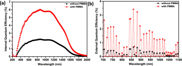
In the case of without PMMA encapsulation, the carbon-based device exhibits the maximum IQE value of ∼2% at a wavelength of 880 nm, which is massively improved to 6% upon encapsulation of PMMA, as shown in Figure 4a. Besides, the EQE was measured for devices with and without PMMA encapsulation, which exhibited a maximum EQE of 0.7 and 3.5%, respectively, at a wavelength of 880 nm in the NIR region, as shown in Figure 4b. The obtained EQE results are comparable to the previously published carbon-based SC-related works.15,42 The results demonstrate that taking advantage of the PMMA encapsulation in the device can be a promising strategy to improve the IQE and EQE and further enhance the overall efficiency of the device. It can be predicted that the semiconducting CNTs might be efficiently dissociated by forming a planar heterojunction between CNT-wrapped C60 molecules that resulted in efficient dissociation of photogenerated excitons in the CNTs and the subsequent collection of free electrons and holes.42 The possible reasons for this type of EQE characteristics for the loss mechanism that may result in <100% efficiency are: (1) wrapping around the surface of the CNTs which may behave as a tunnel barrier that decreases the rate of electron transfer from the CNTs to the C60 molecules, (2) excess PMMA embedded in the film might also function as an electron barrier, and (3) defects associated with the CNT can accelerate the photogenerated electron–hole pair recombination. All these factors thus retard sufficient electron mobility and result in exciton recombination prior to dissociation and electron transfer.43,44 However, a much deeper understanding is required for this type of EQE signals. Further work is underway to understand the role of PMMA in interfacial energy alignment, interfacial electronic structure, and charge transfer (carrier-collection) processes in our system.
Figure 4.
(a) IQE plots of the optimized device at the wavelength of 200–2000 nm and (b) EQE plots of the optimized device in the NIR region for carbon-based SCs with and without PMMA encapsulation.
3.4. Proposed Mechanism of Carbon-Based SCs
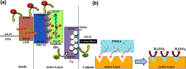
Figure 5a exhibits a schematic band energy diagram of carbon-based SCs. The cells’ construction supported the highest occupied molecular orbital (HOMO) and the lowest unoccupied molecular orbital (LUMO) of different carbon allotropes to extract and collect holes to the external circuit, respectively.45 On sunlight illumination, the GQDs are responsible for the electron–hole separation, and the SWCNT architecture facilitates the electron transport in the SC. Also, this kind of SC may exhibit an energetic relationship between the HOMO and the LUMO, resulting in donor–acceptor charge transfer resonance theory. By utilizing this donor–acceptor sensitization, the carbon materials became capable of generating photocurrents. This kind of cell can be responsible to form a type I heterojunction, which allows the exciton dissociation process.15,46 Besides, as we have mentioned earlier, the PMMA encapsulation protects the cathode interface and ambient deterioration of the active layer by restricting moisture and oxygen diffusion. The role of PMMA is also to fill out the unwanted voids that originated from the solution-processed layer deposition in the cell. These voids can act as a trapped state to disrupt the electron mobility (Figure 5b). In order to eliminate these voids, the PMMA layer penetrates the gaps between active layers, which retard the moisture or oxygen penetration (Figure 5b). Therefore, the PCE is improved because of the reduction of charge loss. The improvement made by carbon materials in the device stability arises from two aspects such as the “barrier effect” provided by the carbon electrode and the “tolerance effect” against moisture and oxidation corrosion.15
Figure 5.
Schematic representation of (a) various carbon allotropes’ band alignment and (b) probable effect of PMMA layer encapsulation on the active layer for the proposed carbon-based SC.
3.5. Study of PMMA Encapsulation Effect
In order to find out the effect of PMMA encapsulation on these cells, the FTIR measurements were conducted with only PMMA (before encapsulation) and after PMMA encapsulation in the cell, as shown in Figure 6a. The FTIR spectrum of PMMA before encapsulation, as shown in Figure 6a, was used to identify the functional groups present in PMMA. The strong band appearing at 1733 cm–1 in the spectrum of the pure PMMA sample can be attributed to the carbonyl (C=O) group and it shifts to 1722 cm–1 at lower intensities and becomes sharper after encapsulation. The band that appeared within the zone of 1100–1600 cm–1 corresponds to the different vibrational modes of the polycyclic aromatic hydrocarbon bond, and the band at 2951 cm–1 is assigned to the C–OH group in the PMMA molecule before encapsulation. There is a distinctive unsymmetrical splitting along with shifting of these characteristic bonds, which portrays evidence for the occurrence of miscibility of the PMMA layer after encapsulation. This may indicate a possible interruption of the PMMA molecule within the interatomic interaction of the device’s active layer causing promising changes in the vibrational modes.25,47,48 This result supports the passivation from the Lewis-base characteristics of the oxygen atoms present in the carbonyl (C=O) groups of PMMA.
Figure 6.
(a) FTIR spectra of the carbon-based SC before and after PMMA encapsulation. AFM images acquired (b) before and (c) after PMMA encapsulation, respectively.
AFM measured the surface roughness in the active layer of the device both in the absence (shown in Figure 6b) and in the presence (shown in Figure 6c) of the PMMA layer. The active layer before PMMA encapsulation exhibited a greater roughness (Figure 6b) than that after encapsulation (Figure 7c). The AFM image and the corresponding height profile of the active layer before and after encapsulation of PMMA clearly show grain boundaries with a typical size of about 5–10 nm. The roughness factor of the active layer without PMMA was 32.0 ± 1.5 nm and after addition of PMMA was 15.6 ± 1.2 nm, which clearly show the reduction of roughness for the inclusion of PMMA. This result indicates that the solution-processed PMMA filled the voids and active layers’ boundaries, which are key parameters affecting the device performance.
Figure 7.
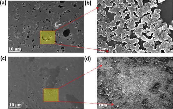
FESEM microstructural images of (a,b) without PMMA and (c,d) with PMMA-encapsulated carbon-based SCs at different magnifications.
The FESEM images (Figure 7a,b) unfold the presence of a substantial number of voids in the SCs without a PMMA layer. In addition, with the PMMA layer, the stability of the device has been improved by reducing the number of voids, as shown in Figure 7c,d. It is worth noting the homogeneous surface coverage of the PMMA layer on the active layer of the cell, and this is expected to favor a direct conduction pathway for rapid electron transport and boosting the photocurrent. As a result, superior encapsulation of PMMA has enhanced the overall device performance compared to the device without encapsulation.
Table 2 indicates the comparative performance from the other published report on carbon-based cell performance. An improvement trend in the photovoltaic performance was found for conjugated polymers based on polystyrene, polythiophene, and so forth compared to other regular forms of carbon allotropes. The obtained results of this work are competitive than the previously published results of the all-carbon-based SCs (Table 2).
Table 2. Reported Performance of Carbon-Based SCs with an Active Area of <0.2 cm2a.
| sl. no. | device architecture | PCE (%) | reference |
|---|---|---|---|
| 1. | ITO-PEDOT/CNTs-C60/Ag rGO/P3DDT/CNTs | 0.46 | (15) |
| 4.71 × 10⁻³ | |||
| 2. | C70/SWCNTs/rGO + e-C70 | 0.85 | (6) |
| 3. | PC70BM/SWCNTs/rGO | 1.3 | (37) |
| 4. | Graphene/PEN/PMMA/P3HT:PCBM/CNTs | 0.63 | (49) |
| 5. | DWNTs/n-Si | 0.82 | (50) |
| 6. | ITO/NTs/C60/BCP/Ag | 0.60 | (51) |
| 7. | P3HT/C60-SWCNTs | 0.57 | (52) |
| 8. | CNTs-P3OT/n-Si | 0.18 | (53) |
| 9. | FTO/rGO/SWCNTs/Graphene QDs/C60/PMMA/Carbon Black | 1.15 | current work |
ITO: indium-doped tin oxide, SWCNTs: single-walled carbon nanotubes, P3DDT: poly(3-dodecylthiophene-2,5-diyl), PEDOT: poly(3,4-ethylenedioxythiophene), PCMB: phenyl-C61-butyric acid methyl ester, P3OT: poly(3-octylthiophene), P3HT: poly(3-hexylthiophene), BCP: bathocuproine.
3.6. Thermal and Visual Comfort Analyses Using Carbon-Based SCs
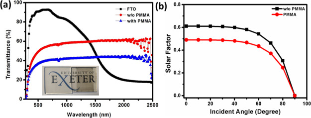
It is also interesting to notice the transmittance spectra of the fabricated films. The effective performance can satisfy the compromise between the efficiency and the transparency of the cell. As per Figure 8a, the carbon cell shows the transparency of ∼50% in the visible region (380–780 nm). The digital image of the fabricated carbon-based cell was also given before the deposition of PMMA and the carbon black layer along with the bare FTO in the inset of Figure 8a. Realization of the semitransparent SC is possible by band gap tuning of SC materials, which maintains the trade-off between the cell transparency and efficiency. Therefore, the recommended transparency value has been observed for both the visible transparency and solar transparency cases for this cell, which has been applied in BIPV applications.
Figure 8.
(a) Transmittance spectra of carbon-based devices with and without (w/o) PMMA addition compared with the bare FTO glass (inset: corresponding digital images) and (b) solar factor plot for the carbon-based SC with and without PMMA.
For BIPV window applications using this carbon-based SC, visual comfort and solar factor evaluations are essential. The vertically mounted carbon SC window transmits the solar energy into the building interior, which has a diurnal nature and changes with the incident angle. According to the European standard, the solar factor can be evaluated from eq 1.28−30,54
| 1 |
At a normal incident angle, devices without PMMA and with PMMA have 0.61 and 0.41 solar factors, respectively, as shown in Figure 8b. Thus, ∼32% reduction is achievable when enhanced PMMA encapsulation is employed. For hot climatic areas, this reduction can save a considerable amount of building’s air condition load.
When carbon materials are present, penetration of daylight through a carbon-based BIPV window may create different light spectra in indoor space. Variation of this spectrum may cause an impact on the building occupants’ comfort. Visual comfort is analyzed by evaluating the color properties, which include the color rendering index (CRI) and the correlated color temperature (CCT), as described in eqs 2 and 3, respectively.55,56 An allowable CCT should have temperatures between 3000 and 7500 K, which is equivalent to that of a blackbody source. CRI values above 90 are considered acceptable, while CRI above 95 and close to 100 are considered to have an outstanding visual quality.57,58 For these cells with and without PMMA, the CRI values are 90 and 95, respectively. Table 3 lists the essential BIPV window parameters.
| 2 |
| 3 |
Table 3. Comparative Study of Color Properties and Transmittance for Carbon SCs.
| device | CRI | CCT | SF | visible transmittance (%) | solar transmittance (%) |
|---|---|---|---|---|---|
| without (w/o) PMMA | 96 | 5799 | 0.61 | 51 | 56 |
| with PMMA | 95 | 5937 | 0.49 | 38 | 41 |
Adopting a greener strategy by using carbon nanostructures can limit the negative environmental impact (reduce the use of toxic organic solvents), and at the same time, the degree of contamination of these carbon materials. The demonstration of light-enhanced ion migration between the layers in the device is also important and will be interesting to study for further research.
Thus, implementation of different carbon allotropes exhibits some added benefit for their widespread applications of SCs because of the identifying functionality of the surface, different morphologies, tuning band gap, and low-cost mass fabrication. All these combinations, therefore, imply a new family of semiconductor devices suitable for various optoelectronic applications. Although there is an important trade-off between the efficiency and the transparency of the device, a more extensive study is further needed for a better understanding.
4. Conclusions
In conclusion, solution-processed sequential fabrication of an FTO/r-GO/SWCNTs/GQDs/C60/carbon black-based device was performed, and their photovoltaic performance was studied. Incorporation of the PMMA layer exhibited a maximum PCE of 1.15% compared to that without the PMMA device (0.56%). Moreover, it is evident that the PCE of the PMMA-based carbon SC device decreased by only about 12% after 1000 h of exposure under moisture ambient conditions. The PMMA layer acts as an encapsulation to the carbon cell, which provides enhanced efficiency and stability to the device. Added benefits such as low-cost materials and a solution-based manufacturing route are therefore expected to integrate the carbon allotropes for carbon-based SCs. This carbon SC showed 38% visible transmittance that made them suitable for future BIPV window applications. Furthermore, the occupant’s comfort of this device was explored by performing visual and thermal comfort analyses. CCT and CRI were close to the limit to offer visual comfort for buildings’ occupants. This work strongly encourages employing solution-processed photovoltaic material fabrication. An effort has been made to utilizing carbon nanostructures to process and inspire a new solution-processing strategy for the futuristic development of organic electronics.
Acknowledgments
The authors acknowledge “Joint UK-India Clean Energy Centre (JUICE)”, which is funded by the RCUK’s Energy Programme (contract no: EP/P003605/1). This work was conducted as part of the JUICE research project. The project funders were not directly involved in the writing of this article.
The authors declare no competing financial interest.
Notes
In support of open access research, all underlying article materials can be accessed upon request via email to the corresponding author.
References
- Turner J. A. A Realizable Renewable Energy Future. Science 1999, 285, 687–689. 10.1126/science.285.5428.687. [DOI] [PubMed] [Google Scholar]
- Kannan N.; Vakeesan D. Solar energy for future world: - A review. Renew. Sustain. Energy Rev. 2016, 62, 1092–1105. 10.1016/j.rser.2016.05.022. [DOI] [Google Scholar]
- Tiwari S. K.; Kumar V.; Huczco A.; Oraon R.; Adhikary A. D.; Nayak G. C. Magical Allotropes of Carbon: Prospects and Applications. Crit. Rev. Solid State Mater. Sci. 2016, 41, 257–317. 10.1080/10408436.2015.1127206. [DOI] [Google Scholar]
- Dresselhaus M. S.; Dresselhaus G.; Saito R.. Nanotechnology in Carbon Materials; Springer: New York, 1999. [Google Scholar]
- Titirici M.-M.; White R. J.; Brun N.; Budarin V. L.; Su D. S.; del Monte F.; Clark J. H.; MacLachlan M. J. Sustainable Carbon Materials. Chem. Soc. Rev. 2015, 44, 250–290. 10.1039/c4cs00232f. [DOI] [PubMed] [Google Scholar]
- Tung V. C.; Huang J.-H.; Kim J.; Smith A. J.; Chu C.-W.; Huang J. Towards Solution Processed All-Carbon Solar Cells: A Perspective. Energy Environ. Sci. 2012, 5, 7810–7818. 10.1039/c2ee21587j. [DOI] [Google Scholar]
- Zhu H.; Wei J.; Wang K.; Wu D. Applications of Carbon Materials in Photovoltaic Solar Cells. Sol. Energy Mater. 2009, 93, 1461–1470. 10.1016/j.solmat.2009.04.006. [DOI] [Google Scholar]
- Brennan L. J.; Byrne M. T.; Bari M.; Gun’ko Y. K. Carbon Nanomaterials for Dye-Sensitized Solar Cell Applications: A Bright Future. Adv. Energy Mater. 2011, 1, 472–485. 10.1002/aenm.201100136. [DOI] [Google Scholar]
- Badenhorst H. A Review of the Application of Carbon Materials in Solar Thermal Energy Storage. Sol. Energy 2019, 192, 35–68. 10.1016/j.solener.2018.01.062. [DOI] [Google Scholar]
- Chen M.; Shao L.-L. Review on the Recent Progress of Carbon Counter Electrodes for Dye-Sensitized Solar Cells. Chem. Eng. J. 2016, 304, 629–645. 10.1016/j.cej.2016.07.001. [DOI] [Google Scholar]
- Tune D. D.; Flavel B. S. Advances in Carbon Nanotube-Silicon Heterojunction Solar Cells. Adv. Energy Mater. 2018, 8, 1703241. 10.1002/aenm.201703241. [DOI] [Google Scholar]
- Ferguson V.; Silva S. R. P.; Zhang W.; Zhang W. Carbon Materials in Perovskite Solar Cells: Prospects and Future Challenges. Energy Environ. Mater. 2019, 2, 107–118. 10.1002/eem2.12035. [DOI] [Google Scholar]
- Meng F.; Liu A.; Gao L.; Cao J.; Yan Y.; Wang N.; Fan M.; Wei G.; Ma T. Current Progress in Interfacial Engineering of Carbon-Based Perovskite Solar Cells. J. Mater. Chem. A 2019, 7, 8690–8699. 10.1039/c9ta01364d. [DOI] [Google Scholar]
- Koltun M.; Faiman D.; Goren S.; Katz E. A.; Kunoff E.; Shames A.; Shtutina S.; Uzan B. Solar Cells from Carbon. Sol. Energy Mater. Sol. Cell. 1996, 44, 485–491. 10.1016/s0927-0248(96)00051-7. [DOI] [Google Scholar]
- Ramuz M. P.; Vosgueritchian M.; Wei P.; Wang C.; Gao Y.; Wu Y.; Chen Y.; Bao Z. Evaluation of Solution-Processable Carbon-Based Electrodes for All-Carbon Solar Cells. ACS Nano 2012, 6, 10384–10395. 10.1021/nn304410w. [DOI] [PubMed] [Google Scholar]
- Lee B.; Buchholz D. B.; Chang R. P. H. An All Carbon Counter Electrode for Dye Sensitized Solar Cells. Energy Environ. Sci. 2012, 5, 6941–6952. 10.1039/c2ee02950b. [DOI] [Google Scholar]
- Cai X.; Hou S.; Wu H.; Lv Z.; Fu Y.; Wang D.; Zhang C.; Kafafy H.; Chu Z.; Zou D. All-Carbon Electrode-Based Fiber-Shaped Dye-Sensitized Solar Cells. Phys. Chem. Chem. Phys. 2012, 14, 125–130. 10.1039/c1cp22613d. [DOI] [PubMed] [Google Scholar]
- Novaes F. D.; Rurali R.; Ordejón P. Electronic Transport between Graphene Layers Covalently Connected by Carbon Nanotubes. ACS Nano 2010, 4, 7596–7602. 10.1021/nn102206n. [DOI] [PubMed] [Google Scholar]
- Zhu Z.; Ma J.; Wang Z.; Mu C.; Fan Z.; Du L.; Bai Y.; Fan L.; Yan H.; Phillips D. L.; Yang S. Efficiency Enhancement of Perovskite Solar Cells through Fast Electron Extraction: The Role of Graphene Quantum Dots. J. Am. Chem. Soc. 2014, 136, 3760–3763. 10.1021/ja4132246. [DOI] [PubMed] [Google Scholar]
- Völker S. F.; et al. Fullerene-Based Materials as Hole-Transporting/Electron-Blocking Layers: Applications in Perovskite Solar Cells. Chem.—Eur J. 2018, 24, 8524–8529. 10.1002/chem.201801069. [DOI] [PubMed] [Google Scholar]
- Jørgensen M.; Norrman K.; Gevorgyan S. A.; Tromholt T.; Andreasen B.; Krebs F. C. Stability of Polymer Solar Cells. Adv. Mater. 2012, 24, 580–612. 10.1002/adma.201104187. [DOI] [PubMed] [Google Scholar]
- Ali U.; Karim K. J. B. A.; Buang N. A. A Review of the Properties and Applications of Poly (Methyl Methacrylate) (PMMA). Polym. Rev. 2015, 55, 678–705. 10.1080/15583724.2015.1031377. [DOI] [Google Scholar]
- Yang F.; et al. Roles of Polymer Layer in Enhanced Photovoltaic Performance of Perovskite Solar Cells via Interface Engineering. Adv. Mater. Interfaces 2018, 5, 1701256. 10.1002/admi.201701256. [DOI] [Google Scholar]
- Ahmad J.; Bazaka K.; Anderson L. J.; White R. D.; Jacob M. V. Materials and Methods for Encapsulation of OPV: A Review. Renew. Sustain. Energy Rev. 2013, 27, 107–117. 10.1016/j.rser.2013.06.027. [DOI] [Google Scholar]
- Wang F.; Shimazaki A.; Yang F.; Kanahashi K.; Matsuki K.; Miyauchi Y.; Takenobu T.; Wakamiya A.; Murata Y.; Matsuda K. Highly Efficient and Stable Perovskite Solar Cells by Interfacial Engineering Using Solution-Processed Polymer Layer. J. Phys. Chem. C 2017, 121, 1562–1568. 10.1021/acs.jpcc.6b12137. [DOI] [Google Scholar]
- Han G. S.; Yoo J. S.; Yu F.; Duff M. L.; Kang B. K.; Lee J.-K. Highly Stable Perovskite Solar Cells in Humid and Hot Environment. J. Mater. Chem. A. 2017, 5, 14733–14740. 10.1039/c7ta03881j. [DOI] [Google Scholar]
- Saifullah M.; Gwak J.; Yun J. H. Comprehensive Review on Material Requirements, Present Status, and Future Prospects for Building-Integrated Semitransparent Photovoltaics (BISTPV). J. Mater. Chem. A. 2016, 4, 8512–8540. 10.1039/c6ta01016d. [DOI] [Google Scholar]
- Roy A.; Ghosh A.; Bhandari S.; Selvaraj P.; Sundaram S.; Mallick T. K. Color Comfort Evaluation of Dye-Sensitized Solar Cell (DSSC) Based Building-Integrated Photovoltaic (BIPV) Glazing after 2 Years of Ambient Exposure. J. Phys. Chem. C 2019, 123, 23834–23837. 10.1021/acs.jpcc.9b05591. [DOI] [Google Scholar]
- Ghosh A.; Selvaraj P.; Sundaram S.; Mallick T. K. The Colour Rendering Index and Correlated Colour Temperature of Dye-Sensitized Solar Cell for Adaptive Glazing Application. Sol. Energy 2018, 163, 537–544. 10.1016/j.solener.2018.02.021. [DOI] [Google Scholar]
- Ghosh A.; Bhandari S.; Sundaram S.; Mallick T. K. Carbon counter electrode mesoscopic ambient processed & characterised perovskite for adaptive BIPV fenestration. Renew. Energy 2020, 145, 2151–2158. 10.1016/j.renene.2019.07.119. [DOI] [Google Scholar]
- Shafran E.; Mangum B. D.; Gerton J. M. Energy Transfer from an Individual Quantum Dot to a Carbon Nanotube. Nano Lett. 2010, 10, 4049–4054. 10.1021/nl102045g. [DOI] [PubMed] [Google Scholar]
- Bhandari S.; Roy A.; Ghosh A.; Mallick T. K.; Sundaram S. Performance of WO3-Incorporated Carbon Electrodes for Ambient Mesoscopic Perovskite Solar Cells. ACS Omega 2020, 5, 422–429. 10.1021/acsomega.9b02934. [DOI] [PMC free article] [PubMed] [Google Scholar]
- Leijtens T.; Giovenzana T.; Habisreutinger S. N.; Tinkham J. S.; et al. Hydrophobic Organic Hole Transporters for Improved Moisture Resistance in Metal Halide Perovskite Solar Cells. ACS Appl. Mater. Interfaces 2016, 8, 5981–5989. 10.1021/acsami.5b10093. [DOI] [PubMed] [Google Scholar]
- Ebadi F.; Taghavinia N.; Mohammadpour R.; Hagfeldt A.; Tress W. Origin of Apparent Light-Enhanced and Negative Capacitance in Perovskite Solar Cells. Nat. Commun. 2019, 10, 1574. 10.1038/s41467-019-09079-z. [DOI] [PMC free article] [PubMed] [Google Scholar]
- Kundu S.; Kelly T. L. Improving the Moisture Stability of Perovskite Solar Cells by Using PMMA/P3HT Based Hole-Transport Layers. Mater. Chem. Front. 2018, 2, 81–89. 10.1039/c7qm00396j. [DOI] [Google Scholar]
- Tang B. Z.; Leung S. M.; Peng H.; Yu N.-T.; Su K. C. Direct Fullerenation of Polycarbonate via Simple Polymer Reactions. Macromolecules 1997, 30, 2848–2852. 10.1021/ma961731f. [DOI] [Google Scholar]
- Bernardi M.; Lohrman J.; Kumar P. V.; Kirkeminde A.; Ferralis N.; Grossman J. C.; Ren S. Nanocarbon-Based Photovoltaics. ACS Nano 2012, 6, 8896–8903. 10.1021/nn302893p. [DOI] [PubMed] [Google Scholar]
- Luo Q.; Ma H.; Hou Q.; Li Y.; Ren J.; Dai X.; Yao Z.; et al. All-Carbon-Electrode-Based Endurable Flexible Perovskite Solar Cells. Adv. Funct. Mater. 2018, 28, 1706777. 10.1002/adfm.201706777. [DOI] [Google Scholar]
- Zhu H.; Wei J.; Wang K.; Wu D. Applications of Carbon Materials in Photovoltaic Solar Cells. Sol. Energy Mater. Sol. Cell. 2009, 93, 1461–1470. 10.1016/j.solmat.2009.04.006. [DOI] [Google Scholar]
- Cao Y.; Parker I. D.; Yu G.; Zhang C.; Heeger A. J. Improved Quantum Efficiency for Electroluminescence in Semiconducting Polymers. Nature 1999, 397, 414–417. 10.1038/17087. [DOI] [PubMed] [Google Scholar]
- Thouti E.; Sharma A. K.; Sardana S. K.; Komarala V. K. Internal Quantum Efficiency Analysis of Plasmonic Textured Silicon Solar Cells: Surface Plasmon Resonance and Off-Resonance Effects. J. Phys. D: Appl. Phys. 2014, 47, 425101. 10.1088/0022-3727/47/42/425101. [DOI] [Google Scholar]
- Arnold M. S.; Zimmerman J. D.; Renshaw C. K.; Xu X.; Lunt R. R.; Austin C. M.; Forrest S. R. Broad Spectral Response Using Carbon Nanotube/Organic Semiconductor/C60 Photodetectors. Nano Lett. 2009, 9, 3354–3358. 10.1021/nl901637u. [DOI] [PubMed] [Google Scholar]
- Peumans P.; Yakimov A.; Forrest S. R. Small Molecular Weight Organic Thin-Film Photodetectors and Solar Cells. Appl. Phys. Lett. 2003, 93, 3693. 10.1063/1.1534621. [DOI] [Google Scholar]
- Peumans P.; Bulović V.; Forrest S. R. Efficient Photon Harvesting at High Optical Intensities in Ultrathin Organic Double-Heterostructure Photovoltaic Diodes. Appl. Phys. Lett. 2000, 76, 2650–2652. 10.1063/1.126433. [DOI] [Google Scholar]
- Wang Z.; Dong F.; Shen B.; Zhang R. J.; Zheng Y. X.; Chen L. Y.; et al. Electronic and Optical Properties of Novel Carbon Allotropes. Carbon 2016, 101, 77–85. 10.1016/j.carbon.2016.01.078. [DOI] [Google Scholar]
- Zhou C.; Lin S. Carbon-Electrode Based Perovskite Solar Cells: Effect of Bulk Engineering and Interface Engineering on the Power Conversion Properties. Sol. RRL 2020, 4, 1900190. 10.1002/solr.201900190. [DOI] [Google Scholar]
- Peng J.; Khan J. I.; Liu W.; Ugur E.; Duong T.; Wu Y.; Shen H.; et al. A Universal Double-Side Passivation for High Open-Circuit Voltage in Perovskite Solar Cells: Role of Carbonyl Groups in Poly(methyl methacrylate). Adv. Energy Mater. 2018, 8, 1801208. 10.1002/aenm.201801208. [DOI] [Google Scholar]
- Uddin A.; Upama M. B.; Yi H.; Duan L. Encapsulation of Organic and Perovskite Solar Cells: A Review. Coatings 2019, 9, 65. 10.3390/coatings9020065. [DOI] [Google Scholar]
- Zhang Z.; Lv R.; Jia Y.; Gan X.; Zhu H.; Kang F. All-Carbon Electrodes for Flexible Solar Cells. Appl. Sci. 2018, 8, 152. 10.3390/app8020152. [DOI] [Google Scholar]
- Wei J.; Jia Y.; Shu Q.; Gu Z.; Wang K.; Zhuang D.; et al. Double-Walled Carbon Nanotube Solar Cells. Nano Lett. 2007, 7, 2317–2321. 10.1021/nl070961c. [DOI] [PubMed] [Google Scholar]
- Bindl D. J.; Wu M.-Y.; Prehn F. C.; Arnold M. S. Efficiently Harvesting Excitons from Electronic Type-Controlled Semiconducting Carbon Nanotube Films. Nano Lett. 2011, 11, 455–460. 10.1021/nl1031343. [DOI] [PubMed] [Google Scholar]
- Li C.; Mitra S. Processing of Fullerene-Single Wall Carbon Nanotube Complex for Bulk Heterojunction Photovoltaic Cells. Appl. Phys. Lett. 2007, 91, 253112. 10.1063/1.2827189. [DOI] [Google Scholar]
- Somani S. P.; Somani P. R.; Umeno M. Carbon Nanotube Incorporation: A New Route to Improve the Performance of Organic-Inorganic Heterojunction Solar Cells. Diam. Relat. Mater. 2008, 17, 585–588. 10.1016/j.diamond.2008.01.084. [DOI] [Google Scholar]
- EN 410: Glass in Building—Determination of Luminous and Solar Characteristics of Glazing; NSAI Standards, 2011.
- McCamy C. S. Correlated Color Temperature as an Explicit Function of Chromaticity Coordinates. Color Res. Appl. 1992, 17, 142–144. 10.1002/col.5080170211. [DOI] [Google Scholar]
- de l’Eclairage, CIE . Spectral Luminous Efficiency Function for Photopic Vision. CIE 086-1990; CIE: 1988 2°, 1990. [Google Scholar]
- Ghosh A.; Norton B. Interior colour rendering of daylight transmitted through a suspended particle device switchable glazing. Sol. Energy Mater. Sol. Cell. 2017, 163, 218–223. 10.1016/j.solmat.2017.01.041. [DOI] [Google Scholar]
- Ghosh A.; Mallick T. K. Evaluation of colour properties due to switching behaviour of a PDLC glazing for adaptive building integration. Renewable Energy 2018, 120, 126–133. 10.1016/j.renene.2017.12.094. [DOI] [Google Scholar]


