

Abstract
A high-performance, wide dynamic range, fully-integrated neural interface is one key component for many advanced bidirectional neuromodulation technologies. In this paper, to complement the previously proposed frequency-shaping amplifier (FSA) and high-precision electrical microstimulator, we will present a proof-of-concept design of a neural data acquisition (DAQ) system that includes a 15-bit, low-power Delta-Sigma analog-to-digital converter (ADC) and a real-time spike processor based on one exponential component-polynomial component (EC-PC) algorithm. High-precision data conversion with low power consumption and small chip area is achieved by employing several techniques, such as opamp-sharing, multi-bit successive approximation (SAR) quantizer, two-step summation, and ultra-low distortion data weighted averaging (DWA). The on-chip EC-PC engine enables low latency, automatic detection and extraction of spiking activities, thus supporting closed-loop control, real-time data compression and/or neural information decoding. The prototype chip was fabricated in a 0.13/μm CMOS process and verified in both bench-top and In-Vivo experiments. Bench-top measurement results indicate the designed ADC achieves a peak signal-to-noise and distortion ratio (SNDR) of 91.8dB and a dynamic range of 93.0dB over a 10kHz bandwidth, where the total power consumption of the modulator is only 20μW at 1.0V supply, corresponding to a figure-of-merit (FOM) of 31.4fJ/conversion-step. In In-Vivo experiments, the proposed DAQ system has been demonstrated to obtain high-quality neural activities from a rat’s motor cortex and also greatly reduce recovery time from system saturation due to electrical microstimulation.
Keywords: data acquisition, electrical microstimulation, dynamic range, high precision, Delta-Sigma ADC, EC-PC spike processor
I. Introduction
NOWADAYS, bidirectional neuromodulation technologies with simultaneous recording and stimulation are urgently demanded in both neuroscience research and neurobiological disease treatment, such as brain-machine-interface (BMI) experiments, stroke rehabilitation, Parkinson’s disease, epilepsy, and severe depression [1]–[11]. Some recent neural recording experiments show that extracellular spikes are from several μV to several hundreds of μV, local field potentials (LFPs) or power line interferences are at a range of mV, and motion artifacts reach tens of mV [12]–[14]. Thus, a wide system dynamic range is required to simultaneously record LFPs, extracellular spikes, motion artifacts, and power line interferences without saturating circuits. The requirement on system dynamic range is further pushed when supporting more sophisticated neuroscience experiments and clinical applications, where electrical microstimulation is used for probing neural circuitry and identifying networks of neurons. However, large amplitude stimulation artifacts (>100mV) that frequently appear in the experiments/applications [15], [16] will saturate the recording systems. Thus, one key challenge is how to reduce recovery time from system saturation due to electrical microstimulation.
Our previous research works have been carried out step-by-step to solve this problem. In [17]–[19], we have proposed a new frontend neural amplifier structure called frequency-shaping amplifier (FSA), which can inherently reject electrode offset, support full-spectrum recording, and extend system dynamic range by 4.5-bit. In [16], we have developed a high-precision electrical microstimulator with multi-level charge-balanced techniques to reduce residual voltage on the stimulation electrodes, thus accelerating the recovery process of nearby recording electrodes. In [20], [21], we have studied the required system dynamic range for signal digitalization by analyzing the recorded In-Vivo neural data sequences carefully, where the dynamic range of full-spectrum (1-8000Hz) neural data reaches between 11-bit and 15-bit [22]. After using the proposed frequency-shaping technique, the required system dynamic range of the frontend circuits can be reduced to around 10.5-bit (15–4.5=10.5 bits). Another 2–3 bits design margin is demanded to avoid large harmonic distortions and reduce recovery time when considering large amplitude stimulation artifacts. As a result, an analog-to-digital converter (ADC) with a resolution of more than 14-bit is required when acquiring full-spectrum neural activities under electrical microstimulation. One optimal ADC architecture for achieving such a high conversion resolution is to use Delta-Sigma ADC topology. However, the drawback is that this topology usually consumes much more power consumption and circuit area compared to successive approximation (SAR) ADC architectures.
In this work, we will present a complementary data acquisition (DAQ) system for simultaneous neural recording and electrical microstimulation, which includes an area-and-power-efficient Delta-Sigma ADC and an on-chip spike processor. To achieve similar power consumption and circuit area like SAR ADC designs, several techniques are developed in the Delta-Sigma ADC design. 1) The combination of high-linearity metal-insulator-metal (MIM) capacitor type and high-density metal-oxide-semiconductor (MOS) capacitor type is adopted to achieve a good tradeoff between low harmonic distortions and small area cost by selecting the optimal capacitor type for each integrator. 2) Due to the utilization of opamp-sharing technique, a single amplifier is shared by multiple integrators to further reduce total power consumption and circuit area. 3) For multi-bit Delta-Sigma ADC designs, the conventional circuit implementation of a multi-bit quantizer is flash ADC structure, which usually consumes much power consumption and circuit area when the quantization resolution is larger than 4-bit. To overcome this problem, a multi-bit quantizer based on SAR ADC structure is preferred for digitizing the integrators’ output signals [23]. 4) In the feedforward adder block, a two-step summation scheme is developed to achieve a full-scale output swing without consuming much power consumption. 5) To achieve ultra-low distortion performance, a novel data weighted averaging (DWA) technique is proposed to calibrate the capacitor mismatch in the feedback digital-to-analog converter (DAC) block. Besides, a reliable, real-time exponential component and polynomial component (EC-PC) spike processor is developed to analyze the existence probability of extracellular spikes, which can be used for data compression and online neural decoding. Also, the EC-PC spike processor can provide a closed-loop control signal to switch the system operation between two modes: only LFPs recording mode (1–1000Hz) and full-spectrum recording mode (1–8000Hz). Therefore, the EC-PC spike processor can optimize the total power consumption of analog frontend circuits by adjusting sampling frequency, recording bandwidth, and bias current [24], [25].
The rest of this paper is organized as follows. Section II explains why a wide dynamic range DAQ system is required in the simultaneous electrical recording and microstimulation applications. Section III presents the design and circuit implementation of the proposed Delta-Sigma ADC and EC-PC spike processor. Circuit measurement and animal experiment results are given in Section IV. Section V gives the conclusion on this paper.
II. Background and Challenges
Parkinson’s disease affects millions of patients worldwide, and the patients suffer from various forms of motor disability that severely affect their daily life. To manage Parkinson’s symptoms, deep brain stimulation (DBS) is an effective way that is widely used in clinical treatment. In addition, to understand the actual impact of DBS on the target neurons, it is necessary to perform intraoperative electrophysiological recording of subthalamic nucleus (STN) or globus pallidus internus (GPi) in Parkinson’s disease patients during stimulation. In this work, we will propose one super wide dynamic range neural data acquisition system that is suitable for simultaneous brain recording and stimulation.
Fig. 1 presents the conceptual block diagrams of one neural DAQ system with electrical stimulation, which consists of a low-noise neural amplifier, a low-pass filter, a high-precision ADC, a neural processor, an electrical stimulator with charge balance, a field programmable gate array (FPGA), an universal serial bus (USB) interface, and data display on a computer. In some conventional neural DAQ systems [26]–[29], the loop gains of neural amplifier and low-pass filter are usually chosen to be 100V/V and 1–10V/V respectively, and the ADC conversion resolution is from 8-bit to 10-bit. Therefore, due to insufficient dynamic range, these DAQ systems are not capable of acquiring LFPs, extracellular spikes, power line interferences, and motion artifacts at the same time. As a compromise, a majority of these systems acquire either LFPs or extracellular spikes separately. Moreover, they are also not suitable for electrical microstimulation experiments, where large stimulation artifacts will saturate the frontend circuits and the recovery time from system saturation is more than tens of milliseconds.
Fig. 1.

Conceptual block diagrams of one neural DAQ system with electrical stimulation. It includes a low-noise neural amplifier, a low-pass filter, a high-precision ADC, a neural processor, an electrical stimulator with charge balance, an FPGA, an USB interface, and data display on a computer. To reduce total power consumption, the designed neural processor generates a feedback control signal to adjust total loop gain, recording bandwidth, and bias current in the frontend circuits and high-precision ADC.
Fig. 2 (black curve) shows one raw data segment at the ADC output with electrical current stimulation, the data are acquired from a conventional neural interface implementing with discrete components. In the experiments, the recorded signals are digitized by a 12-bit SAR ADC, and the loop gains of neural amplifier and low-pass filter are set to be 100V/V and 2V/V, respectively. In addition, one NeuroNexus probe is used for both neural recording and electrical stimulation. As shown in Fig. 2, large stimulation artifacts appear during anodic phase (1ms) and cathodic phase (1ms), and the recovery time is about 20ms when the stimulation current is chosen to be 64μA.
Fig. 2.

One In-Vivo data segment front the electrical current stimulation experiments, where a conventional neural interface implementing with discrete components is used to acquire the signals. X axis is recording time, and Y axis is ADC output code. The gray curve is expected result after using the proposed design strategies for fast recovery after electrical stimulation.
Several alternative design approaches for wide dynamic range neural recording have been presented in [30]–[32]. 1) Moderate Gain Neural Interface Architecture. To increase system dynamic range for neural interfaces, one simple and efficient method is to reduce the neural amplifier’s gain in the frontend circuits. Therefore, one moderate gain neural interface architecture modified from the conventional architecture is developed to prevent circuit saturation for large input signals. In this architecture, the loop gain of neural amplifier is reduced to 20-30dB, thus a high-precision (13-bit or 14-bit) ADC is required to avoid the ADC noise floor will contribute most of the total input noise. Besides, its system dynamic range is increased by 10-20dB compared to the conventional architecture. However, the high-precision ADC block occupies extra circuit area and power consumption, and the recovery time from system saturation is still long due to very large time constant in the neural amplifier stage. 2) ADC-Direct Neural Interface Architecture. Another neural interface architecture is ADC-direct neural interface that only uses a high-precision ADC (>16-bit) to acquire neural activities, where the system dynamic range is detennined by the ADC resolution. For example, if a 16-bit ADC is used, its system dynamic range is around 16-bit. Although the implementation of this architecture is simple, there are two main limitations. First, it cannot suppress electrode or input signal DC offset, especially under electrical stimulation, which may saturate the architecture and degrade its recording performance. Second, the input impedance of this architecture is not high, especially at low frequencies, which will decrease the recorded data’s SNR and bring in large harmonic distortions. 3) Neural Interface Architecture with Artifact Suppression. Neural interface with artifact suppression is another architecture modified from the conventional version, where one block (artifact extraction) is developed in the digital backend circuits to extract the motion/stimulation artifacts, and the artifacts are subtracted in the analog frontend circuits. Therefore, this architecture can allow wide dynamic range input signals without saturating system. However, signal processing distortions will appear when the artifacts are subtracted from the recorded data. Also, it may not accurately extract and subtract the artifacts in time. Another limitation is that the artifact suppression block will cost extra power consumption and circuit area.
In this paper, we will optimize the DAQ system architecture as shown in Fig. 1 and develop several design strategies for fast recovery after electrical stimulation (Fig. 2, gray curve). First, the proposed FSA structure will be used in the neural amplifier stage to inherently reject electrode DC offset and extend system dynamic range by 4.5-bit. Second, the loop gains of both the neural amplifier and low-pass filter will be reduced, thus the settling time of stimulation artifacts is reduced with same amplifier gain bandwidth and slew rate. Also, the system dynamic range will be further increased when small loop gain frontend circuits (neural amplifier and low-pass filter) are designed together with a high-precision ADC. Third, oversampling technique will be used in both the frontend circuits and high-precision ADC, and larger gain bandwidth and slew rate are demanded to further reduce signal setting, processing, and updating time.
Fig. 3 gives the power spectrum density (PSD) comparison of In-Vivo neural data, frontend circuits’ noise floor, and ADC’s noise floor at the ADC output in Simulink, where the input-referred noise of the frontend circuits is supposed to be 2μV [33], [34], the In-Vivo neural data include electrode-tissue interface noise, and the loop gains of neural amplifier and low-pass filter are set to be 40V/V and 1V/V, respectively. From the noise floor comparison, it is found that an ADC with a resolution of more than 14-bit is demanded in the full-spectrum recording in order to get a minimum 10dB signal-to-noise and distortion ratio (SNDR) at all frequencies. Also, to make sure the ADC’s quantization noise floor will not contribute most of the total input noise, the DAQ system as shown in Fig. 1 requires a higher resolution (>14-bit) ADC. It is well known that Delta-Sigma ADC architecture features both high precision and oversampling, thus it is preferred in this work.
Fig. 3.
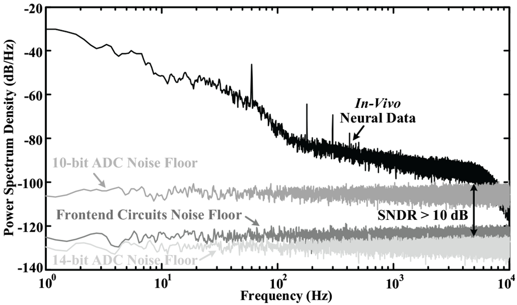
Power spectrum density comparison of In-Vivo neural data, frontend circuits’ noise floor, and ADC’s noise floor at the ADC output in Simulink, where the In-Vivo neural data include electrode-tissue interface noise, and the loop gains of neural amplifier and low-pass filter are set to be 40V/V and 1V/V, respectively.
In addition, to reduce the total power consumption of the proposed DAQ system, an on-chip neural processor is integrated into the high-precision ADC design, which can provide one feedback control signal to adjust the total loop gain (40-320V/V), recording bandwidth (1-1000Hz or 1-8000Hz), and bias current (50-200nA) in the frontend circuits and high-precision ADC.
This paper will focus on the design and implementation of a 15-bit, low-power, area-efficient Delta-Sigma ADC with an embedded EC-PC neural processor, which will be detailedly presented in Section III. Also, the preliminary animal experiment results of the proposed DAQ system under electrical stimulation will be presented in this paper.
III. Circuit Design and Implementation
A. Proposed Modulator Topology
Fig. 4 shows the proposed fourth-order fully-feedforward Delta-Sigma modulator topology with a 16-level quantization and an oversampling ratio (OSR) of 32. To achieve high precision at a low power target, a feedforward loop filter is used instead of a feedback type in order to reduce the output swing of each integrator within 0.1Vpp. Also, the feedforward loop filter gives extra signal pathways from the output of integrators to the quantizer and prevents signal energy leaking into the modulator loop. Besides, multi-bit quantization technique and a local resonator with a coefficient of 1/50 are employed to reduce in-band quantization noise. Compared to one previous work [20], several techniques are developed in this paper to achieve high precision with similar power consumption and circuit area like SAR ADC designs. 1) Because the amplifier in a switched-capacitor (SC) integrator can be powered off during each sampling phase [35], [36]. Thus, opamp-sharing technique is used in the integrators to further reduce power consumption and circuit area by switching the amplifier between two integrators (1st & 2nd integrators or 3rd & 4th integrators). Here, half-delay integrators are adopted due to the requirement of opamp-sharing technique. 2) A 4-bit quantizer based on SAR ADC structure is preferred for digitizing the integrators’ output signals instead of flash ADC structure, which can further reduce power consumption and circuit area. 3) Two-step summation scheme is used in the feedforward adder to achieve a full-scale output swing without consuming much power consumption. Because each integrator has small output swing (within 0.1Vpp), an active adder based on switched-opamp (SO) technique is developed to sum all the integrators’ output while a positive adder is used to get the final sum of input signal IN and active adder’s output. 4) A dual cycle shift (DCS) DWA technique is developed to effectively calibrate the capacitor mismatch in the feedback DAC, thus achieving ultra-low distortion performance.
Fig. 4.

Block diagrams of the proposed fourth-order Delta-Sigma modulator with two-step summation technique and dual cycle shift (DCS) DWA.
B. Complete Modulator Circuit Implementation
To simplify circuit illustration, Fig. 5 shows the single-end circuit implementation of the proposed Delta-Sigma modulator while the actual circuit implementation is fully differential. The designed modulator includes four integrators, one two-step feedforward summation block, one 4-bit SAR ADC, one DCS DWA, one DAC switch control block, and one resonator with a coefficient of 1/50. Here, A1, A2 and A3 are three amplifiers, Vcm is common mode voltage, IN is analog input signal, OUT is 4-bit digital output signal, Pi and Ni (i 1 – 16) are digital control signals for the feedback DAC. The timing diagram is shown in Fig. 6, where Φ1, Φ2, and Φr are non-overlapped clock signals derived from the sampling clock signal Φs (Φ1∩Φ2ȩΦr = Φs, Φ1∪Φ2∪Φr = 0), Φch1 and Φch2 are another two non-overlapped clock signals with a frequency of fs/2 (fs = 1/Φs) for chopper stabilization technique in the first two integrators.
Fig. 5.

Circuit schematic of the proposed fourth-order feedforward Delta-Sigma modulator including four integrators, one two-step feedforward summation block, one 4-bit SAR ADC, one DCS DWA, one DAC switch control block, and one resonator with a coefficient of 1/50. C1–i (i = 1–16) are MIM capacitors used in the input sampling stage and feedback DAC array, C2 – C11 are MOS capacitors adopted in the integrators and local resonator, Cf1 – Cf4 and Ca are MOS capacitors for the implementation of the active adder while Cp is a MIM capacitor used in the positive adder. A1, A2 and A3 are three amplifiers, Vcm is common mode voltage, Vrefp and Vrefn are positive and negative voltage references, IN is analog input signal, OUT is 4-bit digital output signal, Pi and Ni (i = 1– 16) are digital control signals for the feedback DAC.
Fig. 6.

Timing diagram of primary clock signals used in the proposed modulator, where Φ1, Φ2, and Φr are non-overlapped clock signals derived from the sampling clock signal Φs (Φ1∩Φ2∩Φr = Φs, Φ1∪Φ2∪Φr = 0), Φch1 and Φch2 are another two non-overlapped clock signals with a frequency of fs/2 (fs = 1/Φs).
To obtain a good tradeoff among small circuit area, low power consumption, and high precision, several circuit techniques are adopted. First, to simultaneously achieve low harmonic distortions and low circuit area cost, both high-linearity MIM capacitor type and high-density MOS capacitor type are used in this design by selecting the optimal capacitor type for each block. For example, as shown in Fig. 5, MIM capacitors C1–i (i = 1 – 16) and Cp are used in the feedback DAC array and positive adder, while MOS capacitors C2–C11, Cf1–Cf4, and Ca are employed in the integrators, local resonator, and active adder. Second, opamp-sharing technique controlled by Φ1, Φ2, and Φr is used in both A1 and A2 to allow that one single amplifier is shared by two integrators, which could further reduce total power consumption and circuit area. The details of power-efficient amplifier design will be discussed in Section III.C. Third, a local power and area efficient resonator scheme with a coefficient of 1/50 is applied to spread the zeros of noise transfer function (NTF) of the proposed modulator on the unit circle, which could reduce the total quantization noise power in the signal band for the purpose of achieving high precision. The proposed resonator consists of several switches and C9 – C11, and its capability on precision improvement has been demonstrated in [37]. Fourth, a two-step suimnation scheme with both active and positive adders is developed in the feedforward block to achieve a full-scale output swing without consuming much power. Cf1 – Cf4, Ca, and one SO A3 are used in the active adder to sum all the integrators’ output, while Cp and several switches controlled by Ψ1 and Φ2 are adopted in the positive adder to get the final output of the feedforward adder block. Besides, SO technique is used in the active adder for saving power consumption. Fifth, it is known that flash ADC structure usually consumes much power consumption and circuit area when the conversion resolution is more than 4-bit. In this work, a 4-bit SAR ADC is preferred as a multi-bit quantizer for digitizing the recorded signals due to its low power consumption and circuit area cost. Sixth, a new DCS DWA scheme is proposed to calibrate the capacitor mismatch (C1–i, i = 1 ~ 16) in the feedback DAC block to achieve ultra-low distortion performance. The digital output of the DCS DWA block is transferred to a DAC switch control block, which can generate digital control signals Pi and Ni (i = 1 ~ 16) to select C1–i in the feedback DAC to connect with positive voltage reference Vrefp or negative voltage reference Vrefn.
C. Power-Efficient Current-Mirror Amplifiers
Fig. 7 (a)–(c) present the circuit schematics of three power-efficient amplifiers that are used for the implementation of A1, A2, and A3, respectively. All the power-efficient amplifiers are designed based on a single-stage fully-differential current-mirror operational transconductance amplifier (OTA) architecture. To achieve high power efficiency, a Class-AB output stage is added in all the amplifiers. Besides, a cross-coupling structure is built-in to obtain a large voltage gain and also reduce recovery time from the off-state. One common mode feedback (CMFB) circuit block consisting of a switches, two MOS or MIM capacitors, and a singe-stage amplifier is used to make sure the output common mode voltage Vcmo of the amplifier is around Vcm by applying one feedback signal cmfb on two NMOS transistors at the output stage, where Vcmo = (Outp + Outn)/2 and Vcm = (Vrefp + Vrefn)/2.
Fig. 7.

Circuit schematics of three power-efficient amplifiers used in the proposed modulator. All the amplifiers are designed based on a single-stage fully-differential Class-AB current-mirror OTA architecture. Besides, a cross-coupling structure is built-in to obtain a large voltage gain and also reduce recovery time from the off-state, and one CMFB circuit block is used to make sure the output common mode voltage of the amplifier is around Vcm. To achieve high precision with low power consumption, several amplifier configurations are developed for the implementation of A1, A2 and A3, respectively. (a) Amplifier implementation with adjustable current bias and output driving capability for A1. (b) Amplifier implementation with half bias current Ib and quarter output current I0 for A2. (c) Amplifier implementation using switched-opamp (SO) technique and clock-controlled bias circuits for A3. VDD and VSS are power supplies, Vb is bias voltage, Inp and Inn are amplitude input, Outp and Outn are amplitude output, cmfb is control signal from the CMFB block, is the inverse signal of Φ2.
The NTF of one Delta-Sigma modulator features noise shaping when dealing with quantization error, which would gradually relax the design requirements (slew rate, gain bandwidth, and amplifier voltage gain) for each integrator [38]. Therefore, to achieve high precision with low power consumption, different circuit configurations are developed for each amplifier (A1, A2, and A3). For example, Fig. 7 (a) gives an amplifier implementation with adjustable current bias and output driving capability for A1. Because the design requirements of the second integrator are much relaxed compared to the first integrator, thus both bias current Ib and amplifier output current Io are reduced by 50% when the amplifier A1 is connected to the second integrator during phase Φ2. Also, simulation results show the design requirements of the third integrator and fourth integrator are further relaxed, so an amplifier implementation with Ib/2 and Io/4 is developed in Fig. 7 (b) for A2. From the circuit implementation of the active adder as shown in Fig. 5, it is found that the amplifier only needs to operate normally during phase Φ2 and can be turned off during phase Φ1 for power saving. Fig. 7 (c) presents an amplifier implementation using SO technique for A3. Here, two MOS transistor switches controlled by Φ2 and are used to provide clock-controlled power supply voltages VDD and VSS. To reduce the recovery time when the amplifier is restored from the powered-off state, a series MOS switch controlled by Φ2 is added in the bias circuits, which has been demonstrated in our previous work [20]. Besides, MIM capacitor type is used in the CMFB block to achieve good linearity because the output swing of the active adder reaches around 0.2Vpp. The bias current and output current of A3 are chosen to be Ib/2 and Io/2, respectively.
D. Multi-Bit Quantizer Based on SAR ADC Structure
A 4-bit SAR ADC operating at a 4.096MHz top sampling clock clk is designed as a multi-bit quantizer for digitizing the integrators’ output. Fig. 8 (a) shows the complete circuit implementation of the designed 4-bit SAR ADC, where both Vcm-based and set-down switching procedures are used in the feedback capacitor array to achieve high power-and-area efficiency, respectively. Here, the set-down switching procedure employed on the dummy capacitors can provide an extra 1-bit comparison result, thus reducing the number of unit capacitors by 50%. Fig. 8 (b) gives the circuit schematic of a fully-differential dynamic quantizer including a clock-controlled preamplifier and a dynamic comparator with SR latch, where a 4-bit MOS capacitor array is adopted at the output of the clock-controlled preamplifier in order to calibrate the random offset of the quantizer. In the circuit schematic, Vinp and Vinn are the differential input signals of the SAR ADC, Out is the digital output signal of the SAR ADC, Vin+ and Vin− are the differential input signals of the dynamic quantizer, and Vout is the digital output of the dynamic quantizer.
Fig. 8.

Circuit schematic of a 4-bit quantizer based on SAR ADC structure, where both Vcm-based and set-down switching procedures are used in the feedback capacitor array. (a) Complete circuit implementation. (b) Dynamic quantizer with offset calibration. Vinp and Vinn are the differential input signals of the SAR ADC, Out is the digital output signal of the SAR ADC, Vin+ and Vin− are the differential input signals of the dynamic quantizer, Vout is the digital output of the dynamic quantizer, and clk is the top sampling clock.
E. Dual Cycle Shift Data Weighted Averaging
In multi-bit Delta-Sigma modulator designs, traditional DWA is a popular technique to calibrate the capacitor mismatch in the feedback DAC due to its simple circuit implementation. However, if the input of the Delta-Sigma modulator is a DC or low-frequency signal, the mismatch errors of unit capacitors in the feedback DAC will become periodic since the utilization of the capacitor elements is not completely random. As a result, large harmonic distortions will appear in the signal band. To further suppress in-band harmonic distortions, a new DCS DWA technique is developed in Fig. 9. The basic operation principle is to disturb the periodic data sequence randomly and increase the randomness of the control sequence (Pi and Ni, i = 1 ~ 16) when selecting the unit capacitor elements in the feedback DAC. As shown in Fig. 9, several extra circuit blocks in the gray window are added to further process the output sequence of the traditional DWA with low power consumption and small circuit area. In the traditional DWA, a binary to thermometer converter is used to transfer a 4-bit binary input code (B0 ~ B3) into a 16-bit thermometer code (T1 ~ T16), and a 4-stage logarithmic shifter is then adopted to shift the thermometer code based on the control signal in the pointer register. In the DCS DWA, according to the position of split pointer, the output sequence of the traditional DWA is randomly split into two subsequences by a series subset shifter. After that, when B0 is 1 (0), one subsequence will be shifted by 1-bit in a clockwise direction (an anti-clockwise direction) while the other subsequence will be shifted by 1-bit in an anti-clockwise direction (a clockwise direction) every 2n cycles. The final output sequence of the DCS DWA is generated by combining the rotated two subsequences together. In Fig. 9, INi is shifter input, OUTi and OUTi+1 are shifter output, PRTi and PRTi_b (i = 1 ~ 4) are control signals in the traditional DWA, Sf1, Sf1_b, Sf2, and Sf2_b are control signals in the DCS DWA.
Fig. 9.

Block diagrams of the proposed DCS DWA scheme. To further disrupt the data sequence randomly that is used to control the feedback DAC array, a DCS DWA technique is developed to process the output of the traditional DWA. In the traditional DWA, a binary to thermometer converter is used to transfer a 4-bit binary input code (B0 ~ B3) into a 16-bit thermometer code (T1 ~ T16), and a 4-stage logarithmic shifter is then adopted to shift the thermometer code based on the control signal in the pointer register. In the DCS DWA, according to the position of split pointer, the output sequence of the traditional DWA is randomly split into two subsequences by a series subset shifter. After that, when B0 is 1 (0), one subsequence will be shifted by 1-bit in a clockwise direction (an anti-clockwise direction) while the other subsequence will be shifted by 1-bit in an anti-clockwise direction (a clockwise direction) every 2n cycles. The final output sequence of the DCS DWA is generated by combining the rotated two subsequences together. INi is shifter input, OUTi and OUTi+1 are shifter output, PRTi and PRTi_b (i = 1 ~ 4) are control signals in the traditional DWA, Sf1, Sf1_b, Sf2, and Sf2_b are control signals in the DCS DWA.
To better understand the operation principle of the proposed DCS DWA technique, Fig. 10 gives the detailed flow diagram of data sequence when the DCS DWA is fed with an example input code. Through comparing the output data sequences, it is found that the proposed DCS DWA could better disturb the data sequence randomly. Besides, Fig. 11 shows the stimulated in-band harmonic distortion performance in Simulink versus different input signal amplitudes, where the signal frequency is chosen to be 1kHz, the mismatch error of each unit capacitor in the feedback DAC is randomly set to be within ±0.5%, and the maximum in-band tone is calculated based on the difference between peak harmonic distortion and ADC noise floor. Also, several other DWA techniques, such as tradition DWA, pseudo DWA, and split-set DWA, are modeled to make a performance comparison. Simulation results demonstrate that the proposed DCS DWA can provide lowest harmonic distortions at any input signal level.
Fig. 10.

Operation principle illustration of the proposed DCS DWA with an example input code.
Fig. 11.

Simulated in-band harmonic distortion performance of several DWA techniques in Simulink versus different input signal amplitudes. The mismatch error of each unit capacitor in the feedback DAC is randomly set to be within ±0.5%, and the maximum in-band tone is calculated based on the difference between peak harmonic distortion and ADC noise floor.
F. EC-PC Neural Processor
In [24], we first presented the EC-PC spike detection algorithm and also predicted the coexistence of two components (EC and PC) embedded in neural data dynamics, one in the exponential form (noise) and the other in the power form (extracellular spikes). The proposed algorithm was verified in the simulation experiments of In-Vivo data recorded from the hippocampus, cortex surface, and spinal cord. In [25], a 16-channel neural spike detection chip based on the EC-PC algorithm was first implemented in a 0.13μm CMOS process, where the chip takes 12-bit raw ADC output data as input and outputs three data streams simultaneously: LFPs, bandpass filtered neural data, and spiking probability maps. Also, the chip was tested in both In-Vivo experiments for functional verification and bench-top experiments for quantitative performance assessment. In this paper, we will develop an optimized single-channel EC-PC neural processor that can handle wider dynamic range data signal processing, where the 4-bit output of the designed modulator is sent to the processor for further signal processing and a decimation filter is developed to downsample the recorded data and extend the word-length of each data sample from 4-bit to 18-bit. Besides, the designed processor will propose an automatic closed-loop control scheme to reduce the total power consumption of the proposed DAQ system. Circuit area and power consumption optimization techniques will be also developed when synthesizing the proposed processor with digital standard cells.
As shown in Fig. 12, the output of the designed modulator is sent to a digital signal processor for further data processing and analysis, where a decimation filter consisting of one cascaded-integrator-comb (CIC) filter and two half-band filters is used to downsample the recorded data and extend the word-length of each data sample from 4-bit to 16-bit. To reconstruct data without saturating system, a matched digital signal reconstruction filter with offset cancellation is designed, and another 2-bit design margin is given when processing the recorded data. After that, a low-pass filter and a programmable band-pass filter are used to obtain LFPs and spike data, respectively. Usually, there is no neural activity most of the time during neural recording experiments, especially for multiple-channel data acquisition system. Therefore, an EC-PC spike detection algorithm is developed to support real-time data compression and/or neural information decoding by estimating both EC and PC from the band-pass filtered spike data, where the proposed algorithm can predict the presence of neural spikes at any time and give out a spiking activity map for decoding. Because neural data tend to have more compact representations in Hilbert space, the band-pass filtered spike data are sent to a Hilbert transform block to estimate the probability density function (PDF) of the recorded neural data and simplify the EC-PC decomposition. To realize Hilbert transform, fast fourier transform (FFT), and inverse-FFT (IFFT), a Radix-2 single-path delay feedback structure is adopted in this work. The outputs of Hilbert transform module are sent to an EC-PC regression engines, where Hilbert transformed data are first normalized to their estimated variances and accumulated to build histograms. Besides, a fully autonomous training mechanism is realized in the regression engine to extract the EC and PC parameters from the histograms. At last, a spiking probability estimator is developed to generate the spiking probability maps based on the trained EC-PC parameters. According to the detected firing rate and threshold settings, a closed-loop control scheme is implemented to automatically switch the system between the two operation modes (only LFPs recording mode and full-spectrum recording mode). For example, if the detected firing rate is less than 5Hz during a period of 2 seconds, the system will be switched to the LFPs recording mode in next 2 seconds; otherwise, it will continue to operate in the full-spectrum recording mode. In this design, the threshold of the firing rate is adjustable and determined by the real experimental conditions.
Fig. 12.

Implementation diagram of the proposed EC-PC neural processor, which includes a decimation filter, a reconstruction filter with offset removal, a low-pass filter, a band-pass filter, a Hilbert transform block, a spiking probability generator, and a feedback control block.
IV. Measurement Results
The designed ADC and spike processor were fabricated in a one-poly-eight-metal (1P8M) 0.13μm CMOS process, and the chip micrograph is given in Fig. 13. The entire chip area including the pads is 1.35×2.9mm2, and the core circuit area of the designed modulator only occupies 320×420μm2. The output of the designed modulator is sent to the EC-PC spike processor, which consists of a decimation filter, a reconstruction filter with offset removal, a low-pass filter, a band-pass filter, a Hilbert transform block, a spike probability generator, a feedback control block, etc. Fig. 14 shows the experimental evaluation prototype, which consists of the designed chip, an input buffer, a voltage reference block, a clock isolation block, a digital interface, and a chip control block. The prototypes of the proposed FSA and electrical stimulator have been presented in our previous research works [19], [39], which can provide ultra-low noise signal amplification and different current stimulation waveforms/patterns in animal experiments.
Fig. 13.

Chip microphoto of the designed ADC in a 0.13μm CMOS process, where the entire chip area including the pads is 1.35×2.9mm2 and the core circuit area of the designed Delta-Sigma modulator is only 320×420μm2.
Fig. 14.

Evaluation prototype board including the designed ADC and spike processor chip, an input buffer, a voltage reference block, a clock isolation block, a digital interface, and a chip control block.
A. Bench-top Measurement Results
Fig. 15 to Fig. 17 show the bench-top measurement results of the designed ADC, where the ADC operates in the full-spectrum recording mode or only LFPs recording mode. 1) In the full-spectrum recording mode, the DAQ system operates at a 640kHz sampling clock and the power supply voltage is 1.0V. Fig. 15 gives the measured PSD with (black curve) and without (gray curve) the proposed DCS DWA technique when the ADC is fed with a −2.4dB 1.6kHz sinusoidal signal, which clearly shows that the proposed DCS DWA technique could effectively suppress in-band harmonic distortions, especially even-order harmonic distortions. Fig. 16 shows the measured signal-to-noise ratio (SNR) and SNDR over a 10kHz signal bandwidth versus different input amplitudes, where the peak SNR, SNDR, and dynamic range are 92.4dB, 91.8dB, and 93.0dB, respectively. Besides, the total power consumption of the designed modulator including four integrators, bias circuits, one feedfoward adder, one quantizer, one DCS DWA, and one clock generator is 20μW, and the total power consumption of the designed digital signal processor including a decimation filter and an EC-PC spike processor is 52μW. As a result, the designed Delta-Sigma modulator features a very competitive figure-of-merit (FOM) of 31.4fJ/conversion-step. 2) In the only LFPs recording mode, the sampling frequency is reduced to 80kHz, and the power supply voltage is still 1.0V. Fig. 17 gives the measured PSD at the output when the designed ADC is fed with a −1.9dB 200Hz sinusoidal signal, where the measured SNR, SNDR, and dynamic range are 91.3dB, 90.8dB, and 93.0dB over a 1.2kHz signal bandwidth, respectively. Besides, the total power consumption of the designed modulator and digital signal processor is reduced to 3.5μW and 9.5μW, respectively. Table I gives the measurement performance summary of the designed neural Delta-Sigma modulator in comparison with other state-of-the-art publications, and Table II provides the power consumption summary of main blocks in the designed digital signal processor. Table III shows the performance summary of the designed neural processor in comparison with other state-of-the-art works [45]–[47].
Fig. 15.

Measured power spectrum of the designed ADC with/without the proposed DCS DWA when the sampling frequency is 640kHz. The input signal is a −2.4dB 1.6kHz sinusoidal waveform with respect to a 1.0V reference.
Fig. 17.

Measured power spectrum of the designed ADC when the sampling frequency is 80kHz. The input signal is a −1.9dB 200Hz sinusoidal waveform with respect to a 1.0V reference.
Fig. 16.

Measured SNR, SNDR, and dynamic range of the designed ADC versus different input amplitudes, where the sampling frequency is 640kHz, the input signal frequency is 1.6kHz, and the bandwidth is 10kHz.
TABLE I.
Neural Delta-Sigma Modulator performance summary and comparison
| Modulator | [20] | [22] | [40] | [41] | [42] | [43] | [44] | This Work Mode-1 | This Work Mode-2 |
|---|---|---|---|---|---|---|---|---|---|
| Process (nm) | 180 | 600 | 180 | 180 | 130 | 180 | 180 | 130 | 130 |
| Implementation | DT | DT | CT | CT | DT | CT | CT | DT | DT |
| VDD (V) | 1.0 | 2.8 | 1.2/1.8 | 1.8 | 1.2 | 1.8 | 1.8 | 1.0 | 1.0 |
| fs (MHz) | 0.64 | 2 | 0.32 | 2.56 | 0.5 | 20 | N/A | 0.64 | 0.08 |
| Bandwidth (kHz) | 10 | 5 | 4 | 10 | 10 | 10 | 5 | 10 | 1.2 |
| Power (μW) | 13 | 756 | 34.8 | 16.6 | 4.4 | 46.29 | 23 | 20 | 3.5 |
| Dynamic Range (dB) | 87 | 77 | 85.5 | 77.6 | <62 | <65 | 62 | 93 | 93 |
| Peak SNR (dB) | 86.4 | 75.9 | 76.6 | 73.1 | <61 | 51.1 | N/A | 92.4 | 91.3 |
| Peak SNDR (dB) | 85 | 67 | 75.9 | 70.8 | 60.45 | 62.7 | 62 | 91.8 | 90.8 |
| FOMSNDR* (fJ/conv.-step) | 44.7 | 41323 | 853.3 | 292.9 | 255.6 | 2075.6 | 2235.8 | 31.4 | 51.5 |
| FOMDR** (dB) | 175.9 | 145.2 | 166.1 | 165.4 | <155.6 | <148.4 | 145.4 | 180 | 178.4 |
FOMSNDR = Power/[2 * Bandwidth * 2(SNDR–1.76)/6.02]
FOMDR = DR(dB) + 10 * log[Bandwidth/Power], DR is dynamic range
TABLE II.
Power consumption summary of the main blocks in the designed digital signal processor
| Digital Signal Processor | Mode-1 (640kHz) | Mode-2 (80kHz) |
|---|---|---|
| Decimation Filter (μW) | 15 | 2.5 |
| Low-Pass Filter (μW) | 5 | 1 |
| High-Pass Filter (μW) | 8 | 1.5 |
| Hilbert Transform (μW) | 12 | 2 |
| Spike Probability Generator (μW) | 8 | 1.5 |
| Other Blocks (μW) | 4 | 1 |
| Total Power Consumption (μW) | 52 | 9.5 |
TABLE III.
Neural processor performance summary and comparison
| Digital Signal Processor | [45] | [46] | [47] | This Work |
|---|---|---|---|---|
| Process (nm) | 180 | 65 | 65 | 130 |
| VDD (V) | 1.8 | 0.54 | 0.27 | 1.0 |
| fs (kHz) | 30, 120, 240, 960 | 3200 | 480 | 80-640 |
| Channel Number | 1 | 128 | 16 | 1 |
| Power Consumption (μW/channel) | 148 | 0.175 | 4.68 | 9.5-52 |
| Power Density (μW/mm2) | 54.8 | 58.3 | 66.8 | 5.1-28.1 |
| Circuit Area (mm2/channel) | 2.7 | 0.003 | 0.07 | 1.85 |
| Bit per Sample (bit) | N/A | 9 | 8 | 18 |
| Median Clustering Accuracy | 84.5% | 72%-87% | 75% (SNR=0dB-15dB) | 80.8%-96.3% (SNR>2.5dB, Firing Rate>1Hz) |
| Signal Processing Capability | Spike Detection, Feature Extraction, Clustering, Data Compression | Spike Detection, Feature Extraction, Clustering, Data Compression | Spike Detection, Clustering, Data Compression | Data Decimation, Low-Pass Filtering, Band-Pass Filtering, Data Compression, EC-PC Spike Detection, Spiking Probability Mapping, Spike Firing Rate, Recording Bandwidth Adjustment |
When the DAQ system operates in the full-spectrum recording mode, the total power consumption of the designed neural interface is 120μW, which breaks down to 48μW for the frontend circuits (FSA and low-pass filter), 20μW for the ADC, and 52μW for the neural processor. When the system switches to the LFPs recording mode, the total power consumption is reduced to 25μW which includes 12μW for the frontend circuits, 3.5μW for the ADC, and 9.5μW for the neural processor. The averaged power consumption of the neural interface is determined by the closed-loop control parameters and real experiment conditions.
B. Animal Experiment Results
The designed ADC and spike processor chip was also verified in In-Vivo experiments. Fig. 18 shows the animal experiment setup, where a sprague-Dawley rat is anesthetized and placed in a stereotactic frame, a NeuroNexus microelectrode is inserted into the exposed cortical region, and the electrode is connected to an FSA chip. The FSA chip’s output is digitized and analyzed by the prototype board as shown in Fig. 14, and the electrical stimulator chip’s output is connected to the electrode. Fig. 19 shows the recorded extracellular spike activities filtered at 300-8000Hz. The peak-to-peak amplitude of the recorded spike activities is from −90μV to 70μV, and the noise floor is within ±10μV.Fig. 20 gives two recorded spike activity segments and their on-chip signal processing results on spike probability map, spiking firing rate, and adaptive closed-loop control for power saving, where different noise floor and spike shapes of the recorded neural data stream are considered. As shown in Fig. 20 (a) and (b), the spiking firing rate changes from 0Hz to 65Hz. Thus, when the threshold frequency for spiking firing rate is chosen to be 5Hz, an adaptive closed-loop control signal is generated to switch the system operation between the only LFps recording mode and the full-spectrum recording mode. Fig. 21 shows the measured firing rate when the processor is fed with one generated ground-truth data sequence, where the designed EC-PC processor achieves highly accurate firing rate over time.
Fig. 18.

Illustrations of animal experiment setup, where a Sprague-Dawley rat is anesthetized and placed in a stereotypic frame, a NeuroNexus microelectrode is inserted into the exposed cortical region, and the electrode is connected to an FSA chip.
Fig. 19.

One recorded extracellular spike activity segment from a white rat, where the data are filtered at 300-8000Hz.
Fig. 20.

(a) and (b) Spike probability map, firing rate, and operation mode switching of two recorded neural activity segments.
Fig. 21.

(a) One generated ground-truth data segement. (b) Measured firing rate when the processor is fed with the generated ground-truth data.
To demonstrate the proposed DAQ system can reduce the recovery time after electrical stimulation, Fig. 22 gives one recorded data segment at the ADC output, where the neural amplifier is fed with a 64μA, biphasic, 1ms pulse width stimulation current, the DAQ system operates in the full-spectrum recording mode, and the loop gains of neural amplifier and low-pass filter are set to be 40V/V and 1V/V, respectively. The recorded data as shown in Fig. 22 are downsampled to 20kHz. From the measurement results, it is seen that the recovery time after the current stimulation set is around 3ms, which is decreased by around 85% compared to Fig. 2.
Fig. 22.

One recorded In-Vivo data segment with electrical current stimulation, where the proposed DAQ system is used to acquire the signals. X axis is recording time, and Y axis is ADC output code.
Fig. 23 shows two recorded spike activity data segments after electrical current stimulation, where the recorded data are filtered at 300-8000Hz. In Fig. 23 (a), the FSA is fed with a 100μA, biphasic, 1ms pulse width stimulation current while the stimulation current in Fig. 23 (b) is 64μA, biphasic, 1ms pulse width. From the measurement results, it is shown that the proposed DAQ system is capable of acquiring spike activities after electrical stimulation immediately.
Fig. 23.

Two recorded spike activity data segments after electrical current stimulation, where the recorded data are filtered at 300-8000Hz. (a) Neural amplifier is fed with a 100μA, biphasic, 1ms pulse width stimulation current, (b) Neural amplifier is fed with a 64μA, biphasic, 1ms pulse width stimulation current.
V. Conclusion
A wide dynamic range DAQ system consisting of an artifacts-insensitive FSA, a high-precision Delta-Sigma ADC, an on-chip spike processor, and an electrical stimulator with charge balance is designed and implemented in this paper. In the neural Delta-sigma modulator, several circuit techniques, including opamp-sharing technique, multi-bit SAR ADC based quantizer, DCS DWA, two-step summation, and combination of MIM and Mos capacitor types, are used to achieve the target of low power, high precision, and small circuit area. In the neural signal processor, an unsupervised EC-PC neural signal processing algorithm is developed to generate spike probability map, spiking firing rate, and adaptive closed-loop control for further reducing power consumption. The bench-top experiments demonstrate that the designed ADC features very competitive circuit performance, and the animal experiments verify that the designed DAQ system prototype is suitable for simultaneous electrical recording and stimulation applications, which can help reduce the recovery time from the system saturation caused by stimulation artifacts to several milliseconds.
The proposed DAQ prototype presented in this paper is a proof-of-concept design that features fast recovery from system saturation caused by stimulation artifacts. To reduce fabrication and verification cost, only a single-channel Delta-Sigma ADC and a single-channel neural processor are designed and implemented, and the prototypes of our previous FSA and electrical stimulator chips are also used to implement a complete DAQ system for the experiments. The proposed high-precision, wide dynamic range DAQ system targets for evaluating and understanding the effects of DBS in Parkinson’s disease. To reduce circuit area and power consumption, one single neural processor would be developed and shared by multiple recording channels through a digital multiplexer, where the proposed DAQ system includes multiple FSA cores (up to 8 channels), multiple neural Delta-Sigma modulator cores (up to 8 channels), one electrical stimulator, and one neural signal processor.
Acknowledgment
The technology portion of the work was supported in part by National Science Foundation (NSF) CAREER Award #1845709, National Institutes of Health (NIH) R01-MH111413-01, MnDRIVE Program at the University of Minnesota, and a gift fund from Nerves Inc., Dallas, TX, USA The experiment portion of the work was supported in part by Defense Advanced Research Projects Agency (DARPA) under Grants 1198 HR0011-17-2-0060 and N66001-15-C-4016, and NIH R21-NS111214-01.
Biographies

Jian Xu (S’10–M’13) received the B.S. degree and Ph.D. degree from Zhejiang University, Hangzhou, China, in 2007 and 2012, respectively. From March 2011 to July 2012, he held a Visiting Scholar and Research Engineer in the Department of Electrical and Computer Engineering, National University of Singapore, Singapore, where he also worked as a Research Fellow and Senior Research Fellow from 2012 to 2016. He is currently a Researcher 5 in the Department of Biomedical Engineering, University of Minnesota, Minneapolis, MN, USA. His research interests include high-precision low-power data converters, low-power low-noise mixed-signal circuits, wireless power management, & data transmission, biomedical electronics, In-Vivo & In-Vitro experiments, and human clinical trials. His current research works focus on the design and validation of several novel artificial intelligence (AI) based bidirectional neuromodulation devices for human clinical trials.

Anh Tuan Nguyen (S’14) received the B.S. degree (First Class Honour) from National University of Singapore (NUS), Singapore, in 2014. His thesis was awarded the Outstanding Undergraduate Researcher Prize. He is currently pursuing his Ph.D. degree in the Department of Biomedical Engineering, University of Minnesota, Minneapolis, MN, USA. His research focuses on miniaturized, ultra-low power bioelectronics for large-scale neuromodulation applications, including neurostimulators, neural recorders, and MRI compatible devices.

Tong Wu (M’13–S’15) received the B.S. degree from Huazhong University of Science and Technology, Wuhan, China, and the MS degree from Zhejiang University, Hangzhou, China, in 2009 and 2012, respectively. From 2012 to 2015, he was a Research Assistant in the Department of Electrical and Computer Engineering at the National University of Singapore, working on developing algorithms for neural signal processing and VLSI circuit designs. In September 2015, he became a doctoral student in the Department of Biomedical Engineering, University of Minnesota, Twin Cities, MN, USA. His research interests include neuromodulation, on-chip neural computation, machine learning, and VLSI circuit designs.

Wenfeng Zhao (S’13–M’15) received the B.S. and the M.S. degrees from Huazhong University of Science and Technology, Wuhan, China, in 2007 and 2009, respectively, and the Ph.D. degree from the National University of Singapore, Singapore, in 2014. From 2014 to 2016, he was a Research Fellow at the National University of Singapore. In November 2016, he became a Postdoctoral Researcher in the Department of Biomedical Engineering, University of Minnesota, Minneapolis, MN, USA. From January 2020, he is an Assistant Professor of the Department of Electrical and Computer Engineering, Binghamton University, Vestal, NY, USA. His research interests include neural engineering, compressed sensing, ultra-low power VLSI, and in-memory computing.

Diu Khue Luu received the B.S. in Economics from the National University of Singapore, Singapore, in 2015 She graduated with the First Class Honours and a GPA among the top 5% of her class. She is currently pursuing her Ph.D. degree in Biomedical Engineering at the University of Minnesota under the advisory of Prof. Zhi Yang. Her research focuses on the application of advanced computational techniques in designing biomedical devices and systems. She helped develop a mathematical framework to achieve super-resolution in analog-to-digital (ADC) and digital-to-analog converters (DAC), which has been integrated into the neurostimulator design of Yang’s lab. Currently, she studies the deployment of machine learning techniques with the emphasis on deep learning to enable bidirectional communication between the peripheral nervous system and computers. She hopes to contribute to the development of a fully implantable system to enable intuitive control of and sensory feedback from hand prostheses to improve amputees’ well-being.

Zhi Yang (S’04–M’10) received the B.S. degree from Zhejiang University, Hangzhou, China, in 2004, and the M.S. and Ph.D. degrees from the University of California, Santa Cruz, CA, USA, in 2007 and 2010, respectively. He is an Associate Professor of Biomedical Engineering at the University of Minnesota, Minneapolis campus. He is also with MnDrive robotics program and Systems Neuroengineering program at the University of Minnesota. He was an Assistant Professor in the Department of Electrical and Computer Engineering at the National University of Singapore from 2010 to 2015, and in the Department of Biomedical Engineering at the University of Minnesota from 2015 to 2019. His research interests include neural recording and stimulation devices for high-density neural recording, bidirectional neural communication, and on-chip neural signal processing. He has directed 15 funded research projects from federal agencies in USA and Singapore. He has coauthored 70 publications on bioelectronics and signal processing, and edited one book titled Neural Computation, Neural Device, and Neural Prosthesis. He is a recipient of the Best Paper Honorable Mention at ACCV 2009 and the Singapore Young Investigator Award 2012. He is also an invited contributor for a keynote paper in ESSCC 2010, an invited speaker in ISSCC 2012, and a winner of the regional MIT TR35 2014.
Contributor Information
Jian Xu, Department of Biomedical Engineering, University of Minnesota, Minneapolis, MN, 55455, USA.
Anh Tuan Nguyen, Department of Biomedical Engineering, University of Minnesota, Minneapolis, MN, 55455, USA.
Tong Wu, Department of Biomedical Engineering, University of Minnesota, Minneapolis, MN, 55455, USA.
Wenfeng Zhao, Department of Electrical and Computer Engineering, Binghamton University, Vestal, NY, 13902, USA.
Diu Khue Luu, Department of Biomedical Engineering, University of Minnesota, Minneapolis, MN, 55455, USA.
Zhi Yang, Department of Biomedical Engineering, University of Minnesota, Minneapolis, MN, 55455, USA.
References
- [1].Schwarz D, Lebedev M, Hanson T, Dimitrov D, Lehew G, Meloy J, Rajangam S, Subramanian V, Ifft P, Li Z, Ramakrishnan A, Tate A, Zhuang K, and Nicolelis M, “Chronic, wireless recordings of large-scale brain activity in freely moving rhesus monkeys,” Nature Methods, vol. 11, no. 6, pp. 670–676, June 2014. [DOI] [PMC free article] [PubMed] [Google Scholar]
- [2].Burns J, Hsieh YH, Mueller A, Chevallier J, Sriram TS, Lewis SJ, Chew D, Achyuta A, and Fiering J, “High density penetrating electrode arrays for autonomic nerves,” in Proc. 38th Anna. Int. IEEE EMBS Conf., 2016, pp. 2802–2805. [DOI] [PubMed] [Google Scholar]
- [3].Boretius T, Badia J, Pascual-Font A, Schuettler M, Navarro X, Yoshida K, and Stieglitz T, “A transverse intrafascicular multichannel electrode (time) to interface with the peripheral nerve,” Biosensors and Bioelectronics, vol. 26, no. 1, pp. 62–69, Sep 2010. [DOI] [PubMed] [Google Scholar]
- [4].Abdelhalim K, Kokarovtseva L, Velazquez J, and Genov R, “915-MHz FSK/OOK wireless neural recording SoC with 64 mixed-signal FIR filters,” IEEE J. Solid-State Circuits, vol. 48, no. 10, pp. 2478–2493, Oct. 2013. [Google Scholar]
- [5].Xu J, Wang B, Mclaughlin B, Schachther S, and Yang Z, “An integrated sub-scalp eeg sensor for diagnosis in epilepsy,” in IEEE Biomedical Circuits and Systems Conference, 2015, pp. 1–4. [Google Scholar]
- [6].Biederman W, Yeager D, Narevsky N, Koralek A, Carmena J, Alon E, and Rabaey J, “A fully-integrated, miniaturized (0.125 mm2) 10.5 μw wireless neural sensor,” IEEE J. Solid-State Circuits, vol. 48, no. 4, pp. 960–970, April 2013. [Google Scholar]
- [7].Reardon S, “Electroceuticals spark interest,” Nature, vol. 511, p. 18, July 2014. [DOI] [PubMed] [Google Scholar]
- [8].Famrn K, Lift B, Tracey KJ, Boyden ES, and Slaoui M, “Drug discovery: a jump-start for electroceuticals,” Nature, vol. 496, no. 7444, pp. 159–161, April 2013. [DOI] [PMC free article] [PubMed] [Google Scholar]
- [9].Kujawa A, Proudfit GH, and Klein DN, “Neural reactivity to rewards and losses in offspring of mothers and fathers with histories of depressive and anxiety disorders,” Journal of Abnormal Psychology, vol. 123, no. 2, pp. 287–297, May 2014. [DOI] [PMC free article] [PubMed] [Google Scholar]
- [10].Chen R, Canales A, and Anikeeva P, “Neural recording and modulation technologies,” Nature Reviews Materials, vol. 2, no. 16093, pp. 1–16, January 2017. [DOI] [PMC free article] [PubMed] [Google Scholar]
- [11].Yang Z, Xu J, Nguyen AT, Wu T, Zhao W, and Tam WK, “Neuronix enables continuous, simultaneous neural recording and electrical microstimulation,” in Proc. 38th Annu. Int. IEEE EMBS Conf., 2016, pp. 4451–4454. [DOI] [PubMed] [Google Scholar]
- [12].Keshtkaran MR and Yang Z, “A fast, robust algorithm for power line interference cancellation in neural recording,” J. Neural Eng, vol. 11, no. 2, p. 026017, March 2014. [DOI] [PubMed] [Google Scholar]
- [13].Islam M, Rastegarnia A, Nguyen A, and Yang Z, “Artifact characterization and removal from in vivo neural recording,” Journal of Neuroscience Methods, vol. 226, pp. 110–123, April 2014. [DOI] [PubMed] [Google Scholar]
- [14].Buzsaki G, Anastassiou C, and Koch C, “The origin of extracellular fields and currents-EEG, ECoG, LFP and spikes,” Nature Reviews Neitronsci, vol. 13, no. 6, pp. 407–420, June 2012. [DOI] [PMC free article] [PubMed] [Google Scholar]
- [15].Heffer LF and Fallon JB, “A novel stimulus artifact removal technique for high-rate electrical stimulation,” J. Neurosci. Methods, vol. 170, no. 2, pp. 277–284, February 2008. [DOI] [PMC free article] [PubMed] [Google Scholar]
- [16].Nguyen A, Xu J, Tam W, Zhao W, Wu T, and Yang Z, “A programmable fully-integrated microstimulator for neural implants and instrumentation,” in IEEE Biomedical Circuits and Systems Conference, 2016, pp. 472–475. [Google Scholar]
- [17].Xu J, Wu T, Liu W, and Yang Z, “A frequency shaping neural recorder with 3 pF input capacitance and 11 plus 4.5 bits dynamic range,” IEEE Trans. Biomed. Circuits Syst, vol. 8, no. 4, pp. 510–527, August 2014. [DOI] [PubMed] [Google Scholar]
- [18].Xu J, Wu T, and Yang Z, “A new system architecture for future long-term high-density neural recording,” IEEE Trans. Circuits Syst. II, Express Briefs, vol. 60, no. 7, pp. 402–406, July 2013. [Google Scholar]
- [19].Xu J, Nguyen AT, Zhao W, Guo H, Wu T, Wiggins H, Keefer EW, Lint H, and Yang Z, “A low-noise, wireless, frequency-shaping neural recorder,” IEEE J. Emerg. Sel, Topics Circuits Syst, vol. 8, no. 2, pp. 187–200, June 2018. [Google Scholar]
- [20].Xu J, Zhao M, Wu X, Islam MK, and Yang Z, “A high performance delta-sigma modulator for neurosensing,” Sensors, vol. 15, no. 8, pp. 19 466–19 486, August 2015. [DOI] [PMC free article] [PubMed] [Google Scholar]
- [21].Xu J, Islam M, Wang S, and Yang Z, “A 13 μW 87 dB dynamic range implantable ΔΣ modulator for full-spectrum neural recording,” in Proc. 35th Annu. Int. IEEE Engineering in Medicine and Biology Society (EMBC) Conf., 2013, pp. 2764–2767. [DOI] [PubMed] [Google Scholar]
- [22].Qian C, Shi J, Parramon J, and Sanchez-Sinencio E, “A low-power configurable neural recording system for epileptic seizure detection,” IEEE Trans. Biomed. Circuits Syst, vol. 7, no. 4, pp. 499–512, August 2013. [DOI] [PubMed] [Google Scholar]
- [23].Mohamad S, Chao W, Yuan J, and Bermak A, “A power minimized 74 fJ/conversion-step 88.6 dB SNR incremental ΔΣ ADC with an asynchronous SAR quantizer,” in IEEE International Symposium on Circuits and Systems, 2017, pp. 1–4. [Google Scholar]
- [24].Yang Z, Liu W, Keshtkaran MR, Zhou Y, Xu J, Pikov V, Guan C, and Lian Y, “A new EC-PC threshold estimation method for in-vivo neural spike detection,” J. Neural Eng, vol. 9, p. 046017, August 2012. [DOI] [PubMed] [Google Scholar]
- [25].Wu T, Xu J, Lian Y, Khalili A, Rastegarnia A, Guan C, and Yang Z, “A 16-channel nonparametric spike detection ASIC based on EC-PC decomposition,” IEEE Trans. Biomed. Circuits Syst, vol. 10, no. 1, pp. 3–17, February 2016. [DOI] [PubMed] [Google Scholar]
- [26].Qian C, Parramon J, and Sanchez-Sinencio E, “A micropower low-noise neural recording front-end circuit for epileptic seizure detection,” IEEE J. Solid-State Circuits, vol. 46, no. 6, pp. 1392–1405, June 2011. [Google Scholar]
- [27].Lee J, Rhew H, Kipke D, and Flynn M, “A 64-channel programmable closed-loop neurostimulator with 8 channel neural amplifier and logarithmic ADC,” IEEE J. Solid-State Circuits, vol. 45, no. 9, pp. 1935–1945, September 2010. [Google Scholar]
- [28].Lee S, Lee H, Kiani M, Jow U, and Ghovanloo M, “An inductively powered scalable 32-channel wireless neural recording system-on-a-chip for neuroscience applications,” in IEEE Int. Solid-State Circuits Conf. Dig. Tech. Papers, 2010, pp. 120–121. [DOI] [PMC free article] [PubMed] [Google Scholar]
- [29].Liu X, Zhang M, Xiong T, Richardson A, Lucas T, Chin P, Etienne-Cummings R, Tran T, and Spiegel J, “A fully integrated wireless compressed sensing neural signal acquisition system for chronic recording and brain machine interface,” IEEE Trans. Biomed. Circuits Syst, vol. 10, no. 4, pp. 874–883, August 2016. [DOI] [PubMed] [Google Scholar]
- [30].Kim C, Joshi S, Courellis H, Wang J, Miller C, and Cauwenberghs G, “Sub-μVrms-noise sub-μW/channel ADC-direct neural recording with 200-mv/ms transient recovery through predictive digital autoranging,” IEEE J. Solid-State Circuits, vol. 53, no. 11, pp. 3101–3110, November 2018. [Google Scholar]
- [31].Johnson BC, Gambini S, Izyumin I, Moin A, Zhou A, Alexandrov G, Santacruz SR, Rabaey JM, Carmena JM, and Muller R, “An implantable 700μW 64-channel neuromodulation IC for simultaneous recording and stimulation with rapid artifact recovery,” in IEEE Symp. VLSI Circuits Dig. Tech. Papers, 2017, pp. C48–C49. [Google Scholar]
- [32].Mendrela AE, Cho J, Fredenburg JA, Nagaraj V, Netoff TI, Flynn MP, and Yoon E, “A bidirectional neural interface circuit with active stimulation artifact cancellation and cross-channel common-mode noise suppression,” IEEE J. Solid-State Circuits, vol. 51, no. 4, pp. 955–965, April 2016. [Google Scholar]
- [33].Harrison R, Watkins P, Kier R, Lovejoy R, Black D, Greger B, and Solzbacher F, “A low-power integrated circuit for a wireless 100-electrode neural recording system,” IEEE J. Solid-State Circuits, vol. 42, no. 1, pp. 123–133, January 2007. [Google Scholar]
- [34].Wattanapanitch R and Sarpeshkar R, “A low-power 32-channel digitally programmable neural recording integrated circuit,” IEEE Trans. Biomed. Circuits Syst, vol. 5, no. 6, pp. 592–601, December 2011. [DOI] [PubMed] [Google Scholar]
- [35].Cobet C and Knob A, “Noise analysis of switched capacitor networks,” IEEE Trans. Circuits Syst, vol. 30, no. 1, pp. 37–43, January 1983. [Google Scholar]
- [36].Zhu H, Kapusta R, and Kim Y, “Noise reduction technique through bandwidth switching for switched-capacitor amplifier,” IEEE Trans. Circuits Syst. I, Reg. Papers, vol. 62, no. 7, pp. 1707–1715, July 2015. [Google Scholar]
- [37].Xu J, Wu X, Zhao M, Fan R, Wang H, Ma X, and Liu B, “Ultra low-fom high-precision ΔΣ modulators with fully-clocked SO and zero static power quantizers,” in Proc. IEEE Custom Integrated Circuits Conf. (CICC), 2011, pp. 1–4. [Google Scholar]
- [38].Xu J, Wu X, Zhao M, and Shen J, “A 20 μW 95 dB dynamic range 4th-order delta-sigma modulator with novel power efficient operational transconductance amplifier and resonator,” Journal of Zhejiang University SCIENCE C, vol. 12, no. 6, pp. 486–498, June 2011. [Google Scholar]
- [39].Xu J, Guo H, Nguyen AT, Lim H, and Yang Z, “A bidirectional neuromodulation technology for nerve recording and stimulation,” Micromachines, vol. 9, no. 11, p. 538, October 2018. [DOI] [PMC free article] [PubMed] [Google Scholar]
- [40].Tao S and Rusu A, “A power-efficient continuous-time incremental sigma-delta adc for neural recording systems,” IEEE Trans. Circuits Syst. I, Reg. Papers, vol. 62, no. 6, pp. 1489–1498, June 2015. [Google Scholar]
- [41].Shui B, Keller M, Kuhl M, and Manoli Y, “A 70.8 dB 0.0045 mm2 low-power continuous-time incremental delta-sigma modulator for multi-site neural recording interfaces,” in IEEE International Symposium on Circuits and Systems (ISCAS), 2018, pp. 1–4. [Google Scholar]
- [42].Gagnon-Turcotte G, Khiarak MN, Ethier C, Koninck YD, and Gosselin B, “A 0.13-μm CMOS SoC for simultaneous multichannel optogenetics and neural recording,” IEEE J. Solid-State Circuits, vol. 53, no. 11, pp. 3087–3100, November 2018. [Google Scholar]
- [43].Dorigo DD, Moranz C, Graf H, Marx M, Wendler D, Shui B, Herbawi AS, Kuhl M, Ruther P, Paul O, and Manoli Y, “Fully immersible subcortical neural probes with modular architecture and a delta-sigma ADC integrated under each electrode for parallel readout of 144 recording sites,” IEEE J. Solid-State Circuits, vol. 53, no. 11, pp. 3111–3125, November 2018. [Google Scholar]
- [44].Nikas A, Jambunathan S, Klein L, Voelker M, and Ortmanns M, “A continuous-time delta-sigma modulator using a modified instrumentation amplifier and current reuse DAC for neural recording,” IEEE J. Solid-State Circuits, vol. 54, no. 10, pp. 2879–2891, October 2019. [Google Scholar]
- [45].Zamani M, Jiang D, and Demosthenous A, “An adaptive neural spike processor with embedded active learning for improved unsupervised sorting accuracy,” IEEE Trans. Biomed. Circuits Syst, vol. 12, no. 3, pp. 665–676, June 2018. [DOI] [PubMed] [Google Scholar]
- [46].Zeinolabedin SMA, Do AT, Jeon D, Sylvester D, and Kim TH, “A 128-channel spike sorting processor featuring 0.175 μW and 0.0033 mm2 per channel in 65-nm CMOS,” in IEEE Symp. VLSI Circuits Dig. Tech. Papers, 2016, pp. 1–2. [Google Scholar]
- [47].Karkare V, Gibson S, and Markovic D, “A 75-μW, 16-channel neural spike-sorting processor with unsupervised clustering,” IEEE J. Solid-State Circuits, vol. 48, no. 9, pp. 2230–2238, September 2013. [Google Scholar]