Abstract
In this paper, we report anatase and rutile titanium oxide (TiO2) nanoparticulate thin films fabricated on silica and Indium Tin Oxide (ITO) substrates using femtosecond pulsed laser deposition (fs-PLD). Depositions were carried-out at substrate temperatures of 25 °C, 400 °C and 600 °C from anatase and rutile phase target materials. Effect of substrate temperature on the surface morphology, microstructural, optical, and electrical properties of these films were systematically investigated by using various range of measurements such as scanning electron microscopy, (SEM), transmission electron microscopy (TEM), X-ray diffraction (XRD), Raman spectroscopy, Ultraviolet–visible-near infrared (UV–Vis–NIR) spectroscopy, and Hall Effect measurements. It is observed that the TiO2 thin films surface are predominated with nanoparticulates of diameter less 35 nm, which constitute about ~ 70%; while the optical bandgaps and electrical resistivity decrease with increasing substrate temperature. A mixed-phase (anatase/rutile) TiO2 thin film was produced at a substrate temperature of 400 °C when samples are fabricated with anatase and rutile target materials. The results of this study indicate that the structural and crystallinity, optical, and electrical properties can be controlled by varying fs-PLD process parameters to prepare TiO2 thin films, which are suitable for applications in photovoltaics, solar cells, and photo-catalysis.
Subject terms: Engineering, Materials science, Nanoscience and technology
Introduction
Titanium dioxide, TiO2, is among the most studied semiconductor metal oxides in recent years, because of its wide range of applications such as electro-optical devices, self-cleaning and/or antifogging surface coatings, microelectronics, solar cells, photocatalyst, gas sensors, lithium ion batteries, energy harvesting/storage and photovoltaics1–6. The TiO2 nanoparticles and nanorods have unique and improved properties for designing such devices, which can enhance their performance. Nanoparticle’s size, shape, phase, and morphology play significant role in the optical and electrical properties. For instance, Gratzel et al.4 demonstrated low cost and highly efficient dye-sensitized colloidal nanosized TiO2 solar cells, with superior performance over the flat layered photoelectrodes. Similarly, Kuang et al.11 also synthesised TiO2 nanotube arrays with electrochemical anodization technique, for use as a photoanode in the dye-sensitized solar cells. A significant enhancement in photovoltaic performance was observed due to structural arrangement and improved electron transport.
TiO2 exists in three different crystalline structures; anatase (trigonal), rutile (tetragonal) and brookite (orthorhombic)1,7. All the TiO2 polymorphs are low-cost semiconductor materials with fascinating properties, including high transparency, chemical stability, relative hardness and wide optical bandgap range (3.0–3.2 eV)6,9,10. The optical and electrical properties depend mainly on the microstructures, nanostructures, crystallinities and surface area of the TiO2 nanoparticles, as well as their production method. For instance, TiO2 nanoparticles smaller than 20 nm are thermodynamically the stable phase for anatase crystal form11,12, whilst those particle with sizes larger than 20 nm demonstrate high stability for rutile crystal form13. Amorphous or crystalline TiO2 thin films can be fabricated at a very low temperature by the sol–gel method, which would result in low electrons or charge carriers mobilities14. TiO2 thin films with poor electron mobilities will lead to poor device performance for photocatalytic activities, solar cells, and gas sensing applications. As a result, combining heat treatment with a sol–gel technique is used to enhance electrons charge mobilities and consequently improve the performance of such electronic devices. However, at the elevated temperatures, ranging from 200 to 1,000 °C, the phase transformation of TiO2 anatase-to-rutile occurs depending on the fabrication technique8. The phase transformation is irreversible. Very recently, great attention has been given to TiO2 rutile thin films based on various experimental and theoretical investigations owing to its scientific and practical significance. For instance, Chen et al.15 synthesised rutile TiO2 nanorods for photocatalytic analysis and then used to fabricate rutile TiO2 thin films onto F-doped tin-oxide for dye-sensitized solar cells. They demonstrated that the photocatalytic activity upsurges with an increase of hydrothermal time, while fill factor and energy conversion efficiency were found to be ~ 60% and ~ 3.16% for the dye-sensitized solar cells. Furthermore, the mixed-phase of anatase and rutile TiO2 polymorph has a huge advantage for photocatalytic activities and gas sensing device performance since the mixed-phase has improved charge or electron transfer separation and reduces the electron recombination16–18. Besides, the electrons transfer in the mixed-phase lead to anatase–rutile interface trapping site, where the electrons migrate from rutile to anatase in the lower energy anatase lattice (Ti4+) sites19.
TiO2 nanoparticulate thin films have been fabricated by numerous deposition methods; among these are filtered arc deposition20, solution gelation (sol–gel) process21, reactive sputtering method22, chemical vapor deposition23, metal–organic chemical vapor deposition24, and pulsed laser deposition (PLD)25. However, PLD is considered as a promising technique to deposit uniform TiO2 thin films (anatase–rutile mixed phase or nanoparticle-assembled) because the stoichiometric composition of the thin films deposited is identical to the target material used. This technique has several other advantages which include a fast deposition rate, easy to control film growth, film thickness, nanoparticles size or surface roughness while deposition parameters such as energy, temperature, pressure, target-substrate distance can be adjusted to optimise the fabricating process. There have been numerous studies of TiO2 thin films fabricated using nanosecond (ns) PLD26–28 in relation to the ablation plasma plume and characteristics of as deposited films, however, femtosecond (fs) PLD bear potential for further investigation. Even though, the ns-PLD is capable of growing nanostructure film, nevertheless, the nanoparticles are over imposed by larger particles in micron range (micro-particulate) which is disadvantageous for designing miniaturize devices for some of the applications mentioned above. In contrast, fs-PLD technique is appealing to produce uniform nanoparticle size with several advantages over ns-PLD as reported by Kumi-Barimah et al.29 and Semaltianos et al.30. The fs laser materials interaction comprises of ultra-short pulsed length with minimum lattice thermal heating effect, henceforth, the ablation process is quite different from ns-laser. The thin films produce by fs-PLD technique have different morphology, structure and crystallinity depending on the deposition parameters, in particular laser fluence31. For example, fractal TiO2 nanostructures (not thin films) were fabricated by utilising nonthermal fs-PLD under ambient pressure and temperature32,33. They obtained an average nanoparticle diameter below 20 nm, whereas the larger nanoparticles have a diameter above 50 nm. These papers reported that the size of fractal nanostructure distribution depends mainly on the laser fluence and distance between the target-substrate. In addition, these experimental results were also compared to a theoretical model, which confirmed that the fractal nanostructure aggregates are formed through a diffusion mechanism34.
In this paper, we report the production of anatase/rutile mixed-phase and rutile TiO2 nanoparticulate thin films from anatase and rutile TiO2 target materials onto silica and indium tin oxide substrates using fs-PLD technique. The influence of the substrate temperature on the surface morphology, structure, composition, optical and electrical properties of these thin films prepared was systematically studied under various experimental techniques, which have potential for photocatalytic and photovoltaic applications.
Results and discussion
Surface morphology and structural characterisation
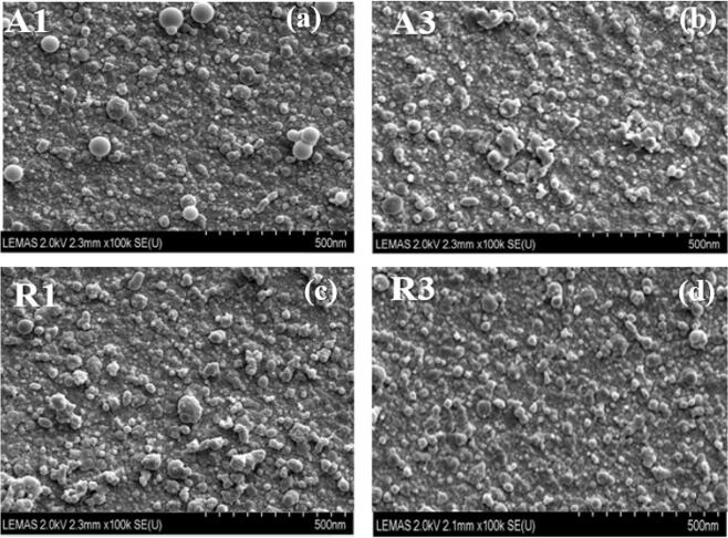
Prior to fabrication of the TiO2 nanoparticulate thin films at various temperatures, optimisation of process parameters such as fs-laser fluence, background oxygen gas pressure, and target-substrate distance were initially determined and implemented. Following this, the optimal processing parameters of the laser fluence for ablation threshold of the TiO2 targets, target-substrate distance, and chamber background oxygen pressure were also found to be 3.34 J/cm2, 80 mm, and 1mTorr. The SEM images of the anatase and rutile TiO2 nanoparticulate thin films as-deposited on silica substrate prepared at various substrate temperatures ranging from room temperature (25 °C) to 700 °C are shown in Fig. 1. An ImageJ software was employed to measure the nanoparticles size distribution statistically using the SEM images shown in Fig. 1.
Figure 1.
Surface morphologies of TiO2 nanoparticulate thin films deposited onto silica substrate by fs-PLD using a scanning emission microscopy (SEM) at various substrate temperatures with 1,280 × 960 pixels and image size of 1,267 nm × 950 nm: anatase thin films: (a) [A1 (25 °C)], (b) [A3 (700 °C)] and rutile thin films: (c) [R1 (25 °C)] (d) [R3 (700 °C)].
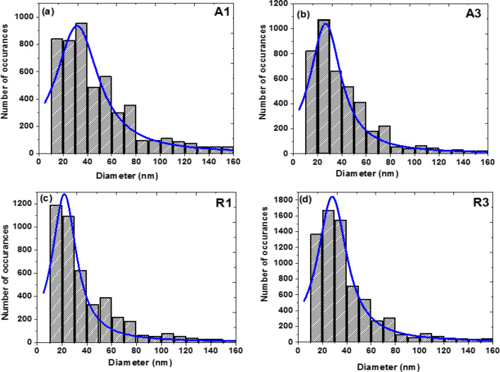
Figure 2a–d illustrates the difference in nanoparticles size distribution (via a histogram) fitted with Lorentzian curve of the SEM image analysis for samples A1, A3, R1, and R3 with each pixel size corresponds to ~ 1 nm. It is important to mention that smaller SEM image magnification was used to determine the particles size such that enough nanoparticles with good resolution can be tested. For anatase samples synthesized (Fig. 1a,b), about ~ 63.9%, ~ 66.8% and ~ 74.2% of nanoparticles have particle sizes of less than 35 nm at 25 °C, 400 °C and 700 °C, respectively. This shows that raising the substrate temperature does not have any significantly influence on the nanoparticle size distribution. For instance, Li et. al.35 synthesised doped and undoped TiO2 nanoparticles deposited on stainless steel mesh by utilising a metalorganic chemical vapour deposition technique. It was demonstrated that the anatase to rutile phase transformation occurred at a substrate temperature of 700 °C along with an observable increase in the nanoparticles size distribution. On the other hand, the nanoparticulate size distribution histograms of our rutile thin films indicate that ~ 69.3%, ~ 70.0%, and ~ 72.5% of the nanoparticulate film have particle sizes under 35 nm for samples fabricated at 25 °C, 400 °C and 700 °C. The size distribution histograms in Fig. 2 reveal slight increasing in number of rutile nanoparticle sizes lower than 35 nm in relation to increasing substrate temperature. This shows that the influence of substrate temperature on particle size is not significant. Moreover, the nanoparticle sizes remain relatively uniform and homogeneously distributed across the entire substrates for both TiO2 nanoparticulate thin films. These results demonstrate that a fs-PLD is more efficient in producing smaller TiO2 nanoparticle size than nanosecond laser PLD. For instance, Walczak et al.26 grown TiO2 nanocrystalline thin films onto silicon substrate by employing nanosecond laser PLD. They noticed that the sample deposited at room temperature showed a small density of aggregation with particles sizes below 500 nm. Whereas those samples fabricated at substrate temperatures at 500 °C and above increased in clusters and aggregation of the nanoparticles with average nanoparticle size of nearly 150 nm at all temperatures. In addition to this, Sanz et al.28 used TiO2 sintered rutile target to fabricate TiO2 thin films onto silicon substrate by utilising three different nanosecond Q-switched Nd:YAG lasers. The aim of this work was to study the influence of laser irradiation wavelength, the substrate temperature, and the presence of oxygen as a background gas pressure. However, the size of microparticulates grown on the silicon substrate ranged from 200 to 2000 nm for substrate temperature spanned from 500 to 700 °C.
Figure 2.
Nanoparticles size distribution histograms obtained from the SEM Images on a grid of 800 × 600 pixels and 100,000 × magnification [1 pixel = 1 nm] shown in Fig. 1 for samples fabricated at different substrate temperature (a) A1 (25 °C), (b) A3 (700 °C), (c) R1 (25 °C) and (d) R3(700 °C).
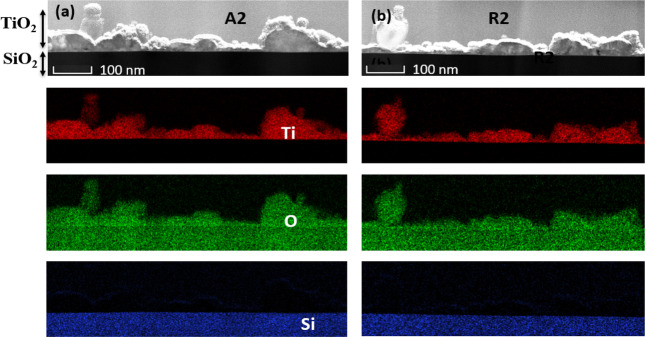
An integrated DualBeam of FIB and FESEM instrument was employed to mill the cross section of the TiO2 nanoparticulate thin films deposited on silica substrate for TEM analysis. The TEM–EDX mappings analysis were also carried out to determine elemental compositions as shown in Fig. 3. These elemental species comprise of Ti, and O are uniformly distributed in the nanoparticulate thin films for samples A2 (Fig. 3a) and R2 (Fig. 3b) as well as other samples not shown here. Furthermore, the plain-view of the TEM cross-sections reveal that the films thicknesses are quite non-uniform, which range from 30 to 125 nm.
Figure 3.
The EDX chemical mapping of the cross-section STEM image for TiO2 nanoparticulate thin films indicating that Ti and O elements are evenly distributed on the SiO2 substrate (lowermost layer): (a) anatase and (b) rutile film deposited at 400 °C.
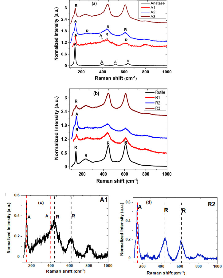
The powdered samples of rutile-target, anatase-target, and nanoparticulate thin films fabricated were initially analysed via Raman spectroscopy for structural identification and distinguishing between various polymorph phases of the TiO2. Figure 4a,b represents a plot of Raman spectra of powdered samples and their corresponding nanoparticulate thin films deposited at various substrate temperatures. For convenience, A and R are denoted as anatase and rutile peaks. In Fig. 4a, the anatase target material has Raman vibrational bands centred at 144, 197, 398, 513, and 638 cm−1, respectively, which correspond to Raman active modes of Eg, Eg, B1g, A1g, and Eg36. However, TiO2 nanoparticulate thin film fabricated at room temperature [A1 (25 °C)] exhibits anatase/rutile mixed-phase with Raman vibration modes peaked at 144 (A), 398 (A), 443 (R), 610 (R) and 803 cm−1 depicted in Fig. 4c for clarity. The weak broad band centred appear around 800 cm−1 is assigned to the silica substrate and Si–O stretching band37,38. The anatase nanoparticulate thin film deposited at 400 °C exhibit mixed-phases of anatase and rutile with Raman frequencies centred at 144 (A), 248 (R), 445 (R), and 612 (R) cm−1 respectively. The prominently intense peak at 144 cm−1 shown in the Raman scattering spectrum confirms the presence of anatase phase while the other peaks are consistent with the rutile polymorph reported39. Furthermore, thin films grown from anatase target at a substrate temperature of 700 °C undergoes a complete phase transformation to rutile polymorph. The Raman modes exhibit characteristics of the rutile peaks in agreement with Raman vibration modes previously reported by Byrne et al.40. In Fig. 4b, Raman spectra of the rutile target and the thin films prepared at different substrate temperatures are presented. The TiO2 rutile target reveals four vibrational bands at 143, 238 (second order effect), 445, 612, and 824 cm−1 which agree with the Raman active modes B1g, Eg, A1g, and B2g41,42. The rutile nanoparticulate thin films were also investigated by using Raman spectroscopy. The Raman vibration bands correlate with rutile polymorph peak. Conversely, the rutile thin film fabricated at a substrate temperature of 400 °C reveals a high intensity at the lower frequency mode, 144 cm−1 (shown as enlarged in Fig. 4d), in the Raman spectrum. This indicates the presence of anatase phase in the rutile nanoparticle-assembled thin film and such a high intensity frequency is not observed in the rutile polymorph.
Figure 4.
Raman scattering spectra of TiO2 targets and TiO2 nanoparticulate thin film deposited on silica substrate at various temperatures (a) anatase [A1 (25 °C), A2 (400 °C) and A3 (700 °C)] and (b) rutile [R1 (25 °C), R2 (400 °C) and R3 (700 °C)]). While (c) A1(25 °C) and (d) R2 (400 °C) correspond to mixed-phase of anatase and rutile shown enlarged.
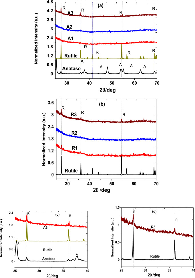
The XRD patterns of the anatase and rutile TiO2 target materials and their corresponding nanoparticle-assembled thin films were also analysed, as this technique can provide structural parameters of crystalline materials’. Figure 5a shows the XRD patterns of the anatase and rutile TiO2 targets along with the anatase nanoparticle-assembled films deposited on silica substrate temperature range from 25 to 700 °C. The TiO2 anatase target exhibits crystalline structure with diffraction peaks at 2θ of 25.24° (101), 37.87° (103), 53.88° (105) and 62.76° (213), respectively, and the International Centre for Diffraction Data (ICDD) card #00-001-0562. On the other hand, the XRD patterns of the TiO2 rutile target are quite intense and narrow with the peak intensities occur at 27.50 (111), 36.04 (101), 41.31 (111), 54.28 (211), and 69.01 (301). The rutile diffraction patterns can be ascribed to ICDD card #00-001-1292 and 01-072-4813. It is worth mentioning that no other TiO2 polymorph was identified in the target anatase and/or rutile patterns. Nonetheless, the anatase nanoparticulate thin films fabricated at 25 °C and 400 °C also reveal no XRD patterns. This could be because the particles deposited on the silica substrate are too thin, henceforth, XRD instrument could not detect the existing of anatase and rutile or mixed phase as observed in the Raman spectroscopy technique. But the sample deposited at 700 °C (A3) reveals three weak crystalline peaks centred at 2θ of 27.56 (110)°, 36.05 (633)°, and 51.71 (220)°, respectively.
Figure 5.
X-ray diffraction patterns of anatase and/or rutile nanoparticles and their corresponding nanoparticles-assembled thin films fabricated by fs-PLD technique at various substrate temperatures: (a) anatase [anatase and rutile targets, A1 (25 °C), A2 (400 °C) and A3 (700 °C)]), (b) rutile [rutile target, R1 (25 °C), R2 (400 °C) and R3 (700 °C)]). While (c) A3 (700 °C) and (d) R3 (700 °C) for 2θ range from 25 to 40° shows XRD pattern enlarged clearly demonstrating with the peaks at 2θ = 27.5° and 36.1°.
A higher substrate temperature utilising to deposit anatase enables rutile phase transformation. According to HighScore database, these crystalline peaks observed in sample A3 agree with TiO2 (rutile), titanium silicate (TiO2–SiO2), and titanium silicon oxide (Ti0.04SiO0.96O2). They also have ICDD diffraction patterns number of #01-075-6234, 00-043-0055, and 04-006-0515. Such phase transformation of anatase to rutile depends on the thermodynamic kinetics and alters the optical properties as well the operation of devices. Alternatively, Fig. 5b illustrates the XRD patterns of target rutile and its corresponding thin films. The weak diffraction patterns of the rutile nanoparticle-assembled thin films peaked at 2θ of 27.50°, 36.05° and 51.71° match with the target rutile peak. Henceforth, the presence of this diffraction peak indicates that the rutile TiO2 deposited at high substrate temperature remains in rutile polymorph without undergoing phase transition. In addition, Fig. 5c, d illustrates the enlarged X-ray diffraction patterns of samples A3 and R3 compared with anatase and rutile targets for 2θ range from 25° to 40°, which clearly reveal rutile diffraction patterns peaked at 2θ = 27.5° and 36.1°.
Optical properties
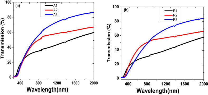
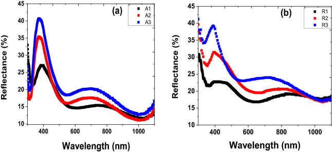
The optical transmittance spectra of as-deposited thin films of anatase and rutile were measured using Perkin Elmer Lambda 905 UV–VIS–NIR Spectrophotometer. These films exhibit good transmission in the spectral range of 250–2,000 nm wavelength. While the reflectance spectra for both samples were recorded with the same Spectrophotometer in a wavelength range from 300 to 1,100 nm. The TiO2 anatase and rutile nanoparticulate thin films increase transmittance with higher substrate temperature in the visible and near-infrared spectra range. However, there is strong absorption in the ultraviolet (uv) and low visible wavelength regions, which is characterised by a sharp drop in optical transmittance and increase reflectance. This can be ascribed to fundamental absorption of TiO2 nanoparticulate thin film layer owing to the transition’s electron from the valence to conduction bands43. This explains why anatase and rutile TiO2 thin film is attractive for photocatalytic and solar cells applications17,18,43. Also, the transmittance at a given temperature for both anatase and rutile phase show similar properties. But the transmittance absorption edge is sensitive to change in substrate temperature, which is shifted to long uv and low visible wavelengths as the substrate temperature increases. For instance, anatase deposited thin films at various substrate temperatures have absorption edge at ~ 318 (A1), 360 (A2), and 351 (A3) nm. Similarly, the rutile samples R1, R2 and R3 have transmittance absorption edge at ~ 328, 357 and 395 mm.
The optical absorption coefficient, α, spectrum was obtained from the transmittance and reflectance spectra shown in Figs. 6 and 7 by employing lambert’s law relationship44:
| 1 |
where T is the transmission, R is the reflectance, and t is the thickness of the film. It worth mentioning that the maximum reflectance of the samples is less than ~ 40% in the 340–420 nm spectral range. Then, Eq. (1) can be expressed as:
| 2 |
Figure 6.
Transmittance of TiO2 nanoparticulate thin films deposited on silica substrate at temperature range from 25 to 700 °C; (a) anatase and (b) rutile.
Figure 7.
Reflectance spectra of the TiO2 thin films (a) anatase and (b) rutile.
The optical bandgap of the nanoparticulate thin films on the silica substrate is estimated by utilising the relationship between α and energy of incident photons known as the Tauc relation44,45;
| 3 |
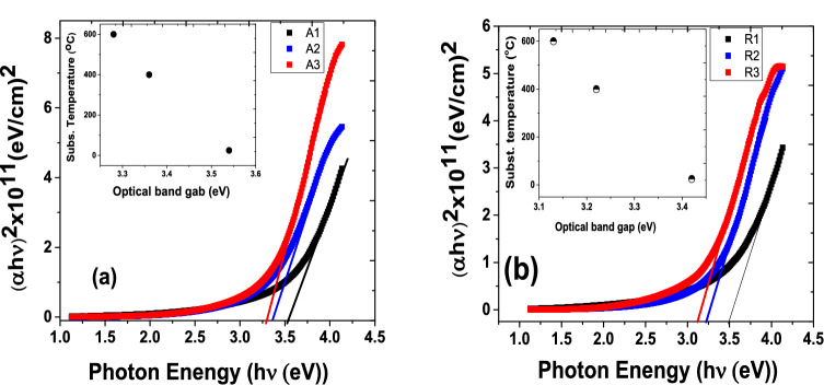
where h is the planck’s constant, υ is frequency, Eg is the optical bandgap, k is a proportionality constant, n is probability factor that takes value of 1/2 (direct allowed), 1 (indirect allowed), 3/2(direct forbidden), or 2 (indirect forbidden) depending on the transition responsible for the absorption, respectively. All the probability power factors, n, in Eq. (2) were tested to plot versus the incident photon energy for the TiO2 anatase and rutile nanoparticulate thin films. Nonetheless, it was found that for direct allowed shows evidence of a perfect fit. Henceforth, Tauc relation of was employed to determine the optical bandgap spectra shown in Fig. 7.
An inset in Fig. 8a shows substrate temperature versus optical bandgap of the anatase nanoparticulate thin films. The optical bandgap increases slight from 3.3 to 3.5 eV with decreasing substrate temperature from 700° to 25°. Similarly, the inset in Fig. 8b represents rutile thin films optical bandgap energies versus substrate temperature, which range from 3.1 to 3.4 eV. It had been reported that an increase in substrate temperature result in decreasing optical bandgap45–49, which is attributed to increase in crystalline size as already discussed in Fig. 2. Moreover, the decrease in optical bandgap in the anatase-target produced thin film is also ascribed to the phase transition into rutile46. In addition, an increased in substrate temperature promotes electron into the conduction band and then generate holes in the valence band, there by producing electron at the tail end of the UV spectrum 50.
Figure 8.
Optical bandgap energies of TiO2 nanoparticle-assembled thin films (a) anatase and (b) rutile.
Electrical properties measurements
Hall Effect measurements of the nanoparticulate thin films prepared on ITO were performed through Van der Pauw method with an excitation current of 10 mA. The excitation current was applied constantly perpendicular to the thin films. Initially, the sheet resistance of each thin film was obtained by measuring the Hall voltage across the Hall field and later used to compute other important parameters listed on Table 1. Table 1 exhibits electrical properties such as sheet resistance (RS), free carrier concentrations (n), doping concentrations (DC), mobility (µ), Hall co-efficient (RH) and resistivity (ρ) of rutile (R) and anatase (A) target prepared thin film on ITO substrate. It can be seen that the resistivity of the as-deposited anatase nanoparticle-assembled thin films on ITO substrate decreases with increasing substrate temperature. Such decrease in the resistivity is a clear indication that the conductivity increases with substrate temperature. As a result, this trend is attributed to increase of carrier mobility and changes in the stoichiometric property of the TiO2 thin film51,52. Besides, the decrease in resistivity can also be ascribed to increase in crystallite size as shown in Fig. 2 as well as decreased in crystallite boundaries and the phase transformation of anatase to rutile, respectively. In the case of the rutile nanoparticle-assembled on ITO, the resistivity of sample fabricated at 400 °C is found to be 138 × 10–6 Ω cm. This could be attributed to formation of anatase–rutile mixed-phase, which has already been discussed in Fig. 3b, d. However, we are unable to measure the sheet resistances and resistivity’s for those samples prepared at substrate temperature of 25 °C and 700 °C.
Table 1.
Hall Effect measurements parameters of the rutile (R2i) and anatase (A2i) thin films on ITO substrates where i = 1, 2, 3 corresponds to substrate temperature of 25, 400, and 700 °C.
| Sample ID | Sheet Resistance (Rs) (Ω/square) | Film Thickness d (10–7 cm) | Hall coefficient, RH (cm3/C) | Mobility (µ) (cm2/V s) | Carrier Conc. (n) (1021 (1/cm3)) | Carrier type | Doping Conc. (Dc) (1016 1/cm2) | Resistivity (ρ) (× 10–6 Ω cm) |
|---|---|---|---|---|---|---|---|---|
| R22 | 11.3 | 122.29 | 2.97 × 10⁻³ | 32.51 | 2.24 | N | 1.70 | 138 |
| A21 | 11.7 | 98.09 | 2.43 × 10⁻³ | 27.38 | 2.57 | N | 1.95 | 114.0 |
| A22 | 11.8 | 71.39 | 2.64 × 10⁻³ | 29.41 | 2.35 | N | 1.80 | 84.3 |
| A23 | 12.5 | 59.7 | 2.72 × 10⁻³ | 28.53 | 2.30 | N | 1.74 | 74.0 |
Conclusion
In conclusion, fs-PLD technique has been successfully used to deposit TiO2 anatase and rutile nanoparticulate thin films on silica and ITO substrates at different temperatures in the range of 25–700 °C. Raman spectral measurements of both samples deposited at substrate temperature of 400 °C confirmed mixed phase TiO2 nanoparticle-assembled thin films. However, anatase target undergoes a complete phase transformation to rutile at substrate temperature of 700 °C. The optical transmittance of anatase and rutile TiO2 thin films deposited onto silica substrate increased in optical absorption region with increasing the substrate temperature. This leads to decrease in optical bandgaps of the nanoparticle-assembled films. The electrical properties of the TiO2 nanoparticle-assembled on ITO substrates were also studied via Hall Effect measurements. The resistivity’s of the anatase thin films on ITO were observed to be dependent on the substrate temperature, which decrease with increasing in substrate temperature. The resistivity of rutile sample deposition on the ITO substrate at a temperature of 400 °C was measured to be 138 × 10–6 Ω.cm, which is ascribed to the presence of anatase–rutile TiO2 mixed-phase. Nevertheless, we were unable to measure the sheet resistance of samples fabricated at 25 °C and 700 °C. Therefore, fs-PLD technique has been used to synthesis and control TiO2 nanostructure thin films, polymorph-phases, optical and electrical properties with huge potential for photovoltaics, antireflection coatings, solar cells, and photo-catalysis applications.
Experimental section
Thin film fabrication
Commercially available TiO2 powders of rutile (> 99.9%) and anatase (99.9%) form were obtained from Santa Cruz Biotechnology and Sigma Aldrich (powder < 5 μm). Both metal-based powder samples were pressed into pallet of 25 mm diameter and 4 mm thickness by using a Speca press set at 17 tonne loads for approximately 20 min. The TiO2 target and silica substrate of dimensions 20 mm × 30 mm × 1.1 mm were mounted into their respective holders with the substrate positioned parallel to the target. The distance between target and substrate was maintained at 80 mm apart. Besides, the silica substrates were initially cleaned in an ultrasonic bath with acetone, followed by isopropyl alcohol and then dried with a clean lens tissue. The target was rastered and rotated at 40 rpm with the substrate rotation rate of 20 rpm. Prior to the depositions, the fs-PLD vacuum chamber was evacuated to a base pressure of ~ 10−5 mTorr, and subsequently injected with high-purity process oxygen gas to adjust the chamber pressure to 1 mTorr. A femtosecond laser equipped with the following specifications was used: wavelength = 800 nm, pulse duration = 100 fs, pulse repetition rate = 1 kHz. The target TiO2 samples were ablated with a laser beam spot diameter of ~ 60 µm and a laser fluence of 3.34 J/cm2 at 60° angle of incidence. The plasma plume consists of nanoparticulate generated from the target is directed perpendicular to the substrate surface. Furthermore, the substrate heater assembly comprises of a water-cooled nickel/gold-plated copper shroud with silicon carbide heating elements. A type K thermocouple provides feedback to the Eurotherm controller, which is inserted through an opening at the top of the heater assembly to monitor the temperature. Once the substrate is mounted in its respective holder, the temperature reading is provided via closed loop temperature feedback to the PID control loop of the Eurotherm controller in conjunction with the heater DC power supply monitors, which provides the substrate temperature calibrated using a pyrometer. Each deposition was limited to 1 h and the substrate temperature was maintained at 25 °C, 400 °C and 700 °C for samples produced from each target material. The samples were denoted as A1 (25 °C), A2 (400 °C), A3 (700 °C) for thin films prepared from the anatase-TiO2 target material and R1 (25 °C), R2 (400 °C), R3 (700 °C) for those obtained from the rutile-TiO2 target material. In addition, the anatase and rutile powders were also deposited on indium tin oxide (ITO) under the same experimental conditions, which were used for electrical properties measurements.
Characterisation
The nanoparticulate thin film morphological features was analysed by Carl Zeiss EVO MA15 scanning electron microscopy (SEM). The SEM images obtained have pixel sizes of 1,280 × 960, image size of 1,268 nm × 950 nm, and a scale bar of 500 nm. These SEM images were initially calibrated with ImageJ software such that the dimensions remain same unit as displayed on the scalar bar. Because, an ImageJ software package can be used to identify each isolated particle deposited on the substrate and allows for measured distributions of all particle’s sizes with maximum efficiency. While composition of the nanoparticles was determined using transmission electron microscopy Energy Dispersive X-ray spectroscopy (TEM–EDX) of cross-section prepared using focused ion beam (FIB) (FEI Helios G4 CX DualBeam). The Energy Dispersive X-ray spectroscopy (EDX) was used to map the chemical composition of the samples for identification of elemental distribution within the planar TEM cross-section of nanoparticles-assembled thin film. The phase transitions of the TiO2 thin films from anatase to rutile and rutile films were characterised via Philips PANalytical X’pert X-ray diffractometer with Cu-Kα radiation (λ = 1.54060A°), and Raman spectroscopy (Renishaw inVia Raman Microscope) with a Ar-ion laser of wavelength 514.5 nm. The Perkin Elmer Lambda 905 UV–visible–NIR spectrometer was employed to record the optical transmission and reflectance through the thin film, which was used to calculate bandgaps of the films. Furthermore, Hall effect study was performed to measure electrical properties such as sheet resistance (RS), free carrier concentrations (n), doping concentrations (DC), mobility (µ), Hall co-efficient (RH) and resistivity (ρ) of TiO2 anatase and rutile thin films deposited on ITO substrate under the same deposition condition as the silica substrate. The four-point probe dc Van der Pauw geometry method was employed to measure sheet resistance/resistivity.
Acknowledgements
The authors acknowledge the financial support from Engineering and Physical Science Research Council (EPSRC) for their financial support through the SeaMatics research Grants (EP/M015165/1 and EP/M022854/1). Thanks to Dr. Zabeada Aslam and Mr. John Harrington, Leeds Electron Microscopy and Spectroscopy (LEMAS) Centre, for support in carrying out the SEM/TEM and FIB measurements.
Author contributions
E.K.B and R.P-J., fabricated the TiO2 thin films and then performed the SEM/TEM images, UV–Vis–NIR transmission and reflectance, Raman spectra, and XRD as well as the data analysis, while E.K.B wrote the manuscript. A.S., U.H., and A.H., carried-out the electrical property measurements and data analysis. While G.J. discussed the results and supervised the project. All the authors edited and reviewed the manuscript.
Data availability
The data that support the findings of this research work are available from the corresponding author upon reasonable request.
Competing interests
The authors declare no competing interests.
Footnotes
Publisher's note
Springer Nature remains neutral with regard to jurisdictional claims in published maps and institutional affiliations.
References
- 1.Tang H, Prasad K, Sanjines R, Schmid PE, Levy F. Cr-doped TiO2 thin films prepared by means of a magnetron co-sputtering process: photocatalytic application. Am. J. Anal. Chem. 2014;5:473–482. [Google Scholar]
- 2.Fujishima A, Honda K. Electrochemical photolysis of water at a semiconductor electrode. Nature. 1976;238(5358):37–38. doi: 10.1038/238037a0. [DOI] [PubMed] [Google Scholar]
- 3.Lin H, Huang CP, Li W, Ni C, Shah SI, Tseng YH. Size dependency of nanocrystalline TiO2 on its optical property and photocatalytic reactivity exemplified by 2-chlorophenol. Appl. Catal. B-Environ. 2006;68:1–11. [Google Scholar]
- 4.Oregan B, Gratzel M. A low-cost, high-efficiency solar cell based on dye-sensitized colloidal TiO2 films. Nature. 1991;353:737–740. [Google Scholar]
- 5.Hagfeldt A, Gratzel M. Studies on the effects of crystallite sizes and scattering layers on the conversion efficiency of dye-sensitized solar cell. J. Power Energy Eng. 2014;2:18–24. [Google Scholar]
- 6.Dette C, Persez-Osorio MA, Kley CS, Punke P, Patrick CE, Jacobson P, Giustino F, Jung Jung S, Kern K. TiO2 anatase with bandgap in the visible region. ACS Nano Lett. 2014;14:6533–6538. doi: 10.1021/nl503131s. [DOI] [PubMed] [Google Scholar]
- 7.Rafieian D, Ogieglo W, Savenije T, Lammertink RGH. Controlled formation of anantase and rutile TiO2 thin films by reactive magnetron sputtering. AIP Adv. 2015;5(1–7):097168. [Google Scholar]
- 8.Hwu Y, Yao YD, Cheng NF, Tung CY, Lin HM. X-ray absorption of nanocrystal TiO2. Nanostruct. Mater. 1997;9(1–8):355–358. [Google Scholar]
- 9.Saleem H, Habib A. Study of bandgap reduction of TiO2 thin films with variation in GO contents and use of TiO2/Graphene composite in hybrid solar cell. J. Alloys Comp. 2016;679:177–183. [Google Scholar]
- 10.Tang H, Lévy F, Berger H, Schmid PE. Urbach tail of anatase TiO2. Phys. Rev. B. 1995;52:7771–7774. doi: 10.1103/physrevb.52.7771. [DOI] [PubMed] [Google Scholar]
- 11.Lamiel-Garcia O, Cuko A, Calatayud M, Illas F, Bromley ST. Predicting size-dependent emergence of crystallinity in nanomaterials: titania nanoclusters versus nanocrystal. Nanoscale. 2017;9:1049–1058. doi: 10.1039/c6nr05788h. [DOI] [PubMed] [Google Scholar]
- 12.Isley SL, Penn RL. Titanium dioxide nanoparticles: effect of sol−gel pH on phase composition, particle size, and particle growth mechanism. J. Phys. Chem. C. 2008;112(12):4469–4474. [Google Scholar]
- 13.Nath A, Laha SS, Khare A. Synthesis of TiO2 nanoparticles via laser ablation at titanium-water interface integrated ferroelectrics. An Int. J. 2010;121(1):58–64. [Google Scholar]
- 14.Hadipour A, Cheyns D, Heremans P, Rand BP. Electrode considerations for the optical enhancement of organic bulk hetro-junction solar cells. Adv. Energy. Mater. 2011;1:930–935. [Google Scholar]
- 15.Chen H-S, Su C, Chen J-L, Yang T-Y, Hsu N-M, Li W-R. Preparation and characterization of pure rutile TiO2 nanoparticles for photocatalytic study and thin films for dye-sensitized solar cells. J. Nanomater. 2010;2011:869618. [Google Scholar]
- 16.Wang SJ. Preparation and characterization of pure rutile TiO2 nanoparticles for photocatalytic study and thin films for dye-sensitized solar cells. J. Vac. Sci. Technol. A. 2008;26(4):869618. [Google Scholar]
- 17.Mohamed MA, Salleh WNW, Jaafar J, Yusof N. Preparation and photocatalytic activity of mixed phase anntase/rutile TiO2 nanoparticles for phenol degradation. J. Teknologi. 2014;70(2):65–70. [Google Scholar]
- 18.Luo Z, Poyraz AS, Kuo C-H, Miao R, Meng Y, Chen S-Y, Jiang T, Wenos C, Suib SL. Crystalline mixed phase (anatase/rutile) mesoporous titanium dioxides for visible light photocatalytic activity. ACS Chem. Mater. 2015;27:6–17. [Google Scholar]
- 19.Hurum DC, Gray KA, Rajh T, Thurnauer MC. Recombination pathways in the Degussa P25 formulation of TiO2: surface versus lattice mechanisms. J. Phys. Chem. B. 2005;109(11):5388–5388. doi: 10.1021/jp045395d. [DOI] [PubMed] [Google Scholar]
- 20.Bendavid A, Martin PJ, Takikawa H. Deposition and modification of titanium dioxide thin films by filtered arc deposition. Thin Solid Films. 2000;360(1–2):241. [Google Scholar]
- 21.Evtushenko YM, Romashkin SV, Trofirmov NS, Chekjlova TK. Optical properties of TiO2 thin films. Phys. Proc. 2015;73:100–107. [Google Scholar]
- 22.Boyadzhiev S, Georgieva V, Rassovska M. Characterization of reactive sputtered TiO2 thin films for gas sensor applications. J. Phys. Conf. Ser. 2010;253(1–6):012040. [Google Scholar]
- 23.Maruyama T, Arai S. Titanium dioxide thin films prepared by chemical vapor deposition. Solar Energy. Mater. Solar Cells. 1992;26(4):323–329. [Google Scholar]
- 24.Saripudin A, Arifin P. Growth mechanism of Co:TiO2 thin film deposited by metal organic chemical vapor deposition technique. IOP Conf. Series: Mater. Sci. Eng. 2016;128(1–5):012046. [Google Scholar]
- 25.Murugesan S, Kuppusami P, Parvathavarthini N, Mohandas E. Pulsed laser deposition of anatase and rutile TiO2 thin films. Surf. Coat. Technol. 2007;201(18):7713–7719. [Google Scholar]
- 26.Walczak M, Oujja M, Marco JF, Sanz M, Castillejo M. Pulsed laser deposition of TiO2: diagnostic of the plume and characterization of nanostructured deposits. Appl. Phys. A. 2008;93:735–740. [Google Scholar]
- 27.Walczak M, Papadopoulou EL, Sanz M, Manousaki A, Marco JF, Castillejo M. Structural and morphological characterization of TiO2 nanostructured films grown by nanosecond pulsed laser deposition. Appl. Surf. Sci. 2009;255:5267–5270. [Google Scholar]
- 28.Sanz M, Walczak M, Oujja M, Cuesta A, Castillejo M. Nanosecond pulsed laser deposition of TiO2: nanostructure and morphology of deposits and plasma diagnosis. Thin Solid Films. 2009;517:6546–6552. [Google Scholar]
- 29.Kumi-Barimah E, Ziarko MW, Bamiedakis N, White IH, Penty RV, Jose G. Erbium-doped glass nanoparticle embedded polymer thin films using femtosecond pulsed laser deposition. Opt. Mater. Express. 2018;8(7):1997–2007. [Google Scholar]
- 30.Semaltianos G, Perrie W, Sharp M, Williams CJ, Edwardson SP, Dearden G, Watkins KG. Nano-particles generation by femtosecond laser ablation. ICALEO Cong. Proc. 2007;N405:114–118. [Google Scholar]
- 31.Mann T, Richards B, Kumi-Barimah E, Mathieson R, Murray M, Ikonic Z, Steenson P, Russell C, Jose G. Femtosecond pulsed laser deposited Er3+-doped zinc-sodium tellurite glass on Si: thin-film structural and photoluminescence properties. AIP Adv. 2019;9(1–10):085324. [Google Scholar]
- 32.Cavaliere E, Benetti G, Celardo GL, Archetti D, Pingue P, Ferrini G, Gavioli L. Aggregation and fractal formation of Au and TiO2 nanostructures obtained by fs-pulsed laser deposition: experiment and simulation. J. Nanopart. Res. 2017;19(1–7):311. [Google Scholar]
- 33.Cavaliere E, Ferrini G, Pingue P, Gavioli L. Fractal TiO2 nanostructures by nonthermal laser ablation at ambient pressure. J. Phys. Chem. C. 2013;117:23305–23312. [Google Scholar]
- 34.Celardo GL, Archetti D, Ferrini G, Gavioli L, Pingue P, Cavaliere E. Evidence of diffusive fractal aggregation of TiO2 nanoparticles by femtosecond laser ablation at ambient conditions. Mater. Res. Express. 2017;4(1–10):015013. [Google Scholar]
- 35.Li W, Ismat Shah S, Huang C-P, Jung O, Nia C. Metallorganic chemical vapor deposition and characterization of TiO2 nanoparticles. Mater. Sci. Eng. B. 2002;96:247–253. [Google Scholar]
- 36.GeorgianaIlie A, Scarisoareanu M, Morjan I, Dutu E, Badiceanu M, Mihailescu I. Principal component analysis of Raman spectra for TiO2 nanoparticle characterization. Appl. Surf. Sci. 2017;417:93–103. [Google Scholar]
- 37.Novikov S, Khriachtchev L. Surface-enhanced raman scattering of silicon nanocrystals in a silica film. Sci. Rep. 2016;6(1–9):27027. doi: 10.1038/srep27027. [DOI] [PMC free article] [PubMed] [Google Scholar]
- 38.Walrafen GE, Krishnan PN. Raman spectrum of a pressure compacted fused silica. J. Chem. Phys. 1981;74(9):5329–5330. [Google Scholar]
- 39.Mazza T, Barhorni E, Piseri P, Milani P. Raman spectroscopy characterization of TiO2 rutile nanocrystals. Phys. Rev. B. 2007;75(1–5):045416. [Google Scholar]
- 40.Byrne C, Fagan R, Hinder S, McCormack DE, Pillai SC. New approach of modifying the anatase to rutile transition temperature in TiO2 photocatalysts. RSC Adv. 2016;6:95232–95238. [Google Scholar]
- 41.Tang H, Prasad K, Sanjines R, Schmid P, Levy F. Electrical and optical properties of TiO2 anatase thin films. J. Appl. Phys. 1994;75:2042–2047. [Google Scholar]
- 42.Berger H, Tang H, Lévy F. Growth and Raman spectroscopic characterization of TiO2 anatase single crystals. J. Cryst. Growth. 1993;130:108–112. [Google Scholar]
- 43.Nikolskaia M, Vildanova S, Kozlov N, Tsvetkov L, Larina OS. Charge transfer in mixed-phase TiO2 photoelectrodes for perovskite solar cells. Sustainability. 2020;12(1–14):788. [Google Scholar]
- 44.Albarkaty KS, Kumi-Barimah E, Craig C, Hewak D, Jose G, Chandrappan J. Erbium-doped chalcogenide glass thin film on silicon using femtosecond pulsed laser with different deposition temperatures. Appl. Phys. A. 2019;125(1):1–8. [Google Scholar]
- 45.Mathews NR, Morales ER, Cortes-Jacome MA, Toledo Antonio JA. TiO2 thin films-influence of annealing temperature on structutal, optical and photocatalytic properties. Sol. Energy. 2009;83:1499–1508. [Google Scholar]
- 46.Sankar S, Gopchandran K. Effect of annealing on the structural, electrical and optical properties of nanostructured TiO2 Thin Films. Cryst. Res. Technol. 2009;44:989–994. [Google Scholar]
- 47.Walczak M, Papadopoulou EL, Sanz M, Manousaki A, Marco JF, Castillejo M. Structural and morphological characterization of TiO2 nanostructured films grown by nanosecond pulsed laser deposition. Appl. Surf. Sci. 2010;255(10):5267–5270. [Google Scholar]
- 48.Reyes-Coronado D, Rodrıguez-Gattorno G, Espinosa-Pesqueira ME, Cab C, Coss RD, Oskam G. Phase-pure TiO2 nanoparticles: anatase, brookite and rutile. Nanotechnol. 2008;19(14):145605. doi: 10.1088/0957-4484/19/14/145605. [DOI] [PubMed] [Google Scholar]
- 49.Kim D, Kim W, Kim S, Hong S. Brookite TiO2 thin film epitaxially grown on (110) YSZ substrate by atomic layer deposition. ACS Appl. Mater. Interface. 2014;6(15):11817–11822. doi: 10.1021/am501656r. [DOI] [PubMed] [Google Scholar]
- 50.Scanlon DO, Dunnill CW, Buckeridge J, Shevlin SA, Logsdail AJ, Woodley SM, Sokol AA. Band alignment of rutile and anatase TiO2. Nat. Mater. 2013;12(9):798–801. doi: 10.1038/nmat3697. [DOI] [PubMed] [Google Scholar]
- 51.Hanini F, Bouabellou A, Bouachiba Y, Kermiche F, Taabouche A, Hemissi M, Lakhdari D. Structural, optical and electrical properties of TiO2 thin films synthesized by sol-gel technique. IOSR J. Eng. 2013;3(11):21–28. [Google Scholar]
- 52.Chiu P-K, Lee CT, Chiang D, Cho WH, Hsiao CN, Chen YY, Huang BM, Yang JR. Conductive and transparent multilayer films for low-temperature TiO2/Ag/SiO2 electrodes by E-beam evaporation with IAD. Nanoscale Res. Lett. 2014;9(1):35. doi: 10.1186/1556-276X-9-35. [DOI] [PMC free article] [PubMed] [Google Scholar]
Associated Data
This section collects any data citations, data availability statements, or supplementary materials included in this article.
Data Availability Statement
The data that support the findings of this research work are available from the corresponding author upon reasonable request.


