

Abstract

We investigate a waveguide-integrated plasmonic graphene photodetector operating based on the hot carrier photo-bolometric effect, which is characterized simultaneously by high responsivity on the scale of hundreds of A/W and high speed on the scale of 100’s of GHz that is limited only by the product of the electronic heat capacitance and thermal resistance. We develop a theory of the bolometric effect originating from the band nonparabolicity of graphene and estimate responsivity due to the bolometric effect, which is shown to significantly surpass the responsivity of the coexisting photoconductive effect, thus convincingly demonstrating the dominance of the bolometric effect. Based on the theory, we propose a novel detector configuration based on a hybrid waveguide that allows for efficient absorption in graphene over a short distance and subsequently a large change of conductivity. The results demonstrate the potential of graphene for high-speed communication systems.
Introduction
On-chip high-speed photodetectors are crucial components in optical communications that convert the absorbed photons into an electrical signal.1,2 Being the last components in the optical links, the detectors must operate with low power if costly amplifiers are to be avoided. They operate beyond 100 GHz and are characterized by low current and high responsivity. Most traditional optoelectronic devices suffer, however, from high power consumption, low operation speed, low responsivity, or large footprint.3 Thus, finding a better design platform is of great interest for the industry and academia. In the last few decades, it has become obvious that further progress can be made through an implementation of new materials,4−6 integration with plasmonics,7−10 or both. Plasmonics can squeeze light much below the diffraction limit, which reduces the device footprint.8,9 Furthermore, a small device volume means a higher density of integration and, simultaneously, lower power consumption, easier heat dissipation, and faster operation speed.8,11−13 During the last few years, some waveguide-integrated plasmonic photodetectors on silicon12−18,24,66 and germanium19,20 have been proposed and fabricated. However, the search for better material platform continues. Graphene is a very promising material for signal modulation and photodetection, owing to its extraordinary transport properties.21−23 Being only one atom thick, it absorbs 2.3% of incident light in a very wide energy spectrum.5,21,22 It has ultrafast carrier dynamics, tunable optical properties, and high carrier mobility, enabling ultrafast conversion of photons or plasmons to electrical current or voltage.25−27 Vice versa, it can convert a received electrical signal onto an optical carrier in this way working as the optical modulator.5,28−31 Moreover, graphene is CMOS-compatible, allowing integration on a wafer scale.3−5 Graphene photodetectors can operate based on photovoltaic,11,32 photo-thermoelectric (PTE),13,33 photo-gaining,34,35 or photo-bolometric (PB)12,32,36−41 effects. The choice of effect depends on a photodetector’s configuration and specific applications.37,42 Bolometers have emerged as the technology of choice because they do not need cooling. Actually, they utilize the temperature-dependent material properties for photodetection; the incident light raises the local electronic temperature of the material, which reduces the resistance of the device and produces a change in the current.42−46 Graphene is well suited for this purpose as it has a small electron heat capacity and weak electron–lattice (e–l) coupling, leading to a large light-induced change in the electron temperature.13,16,25,26 The low density of states and small volume for a given area result in low heat capacity. Simultaneously, the cooling of electrons by acoustic phonons is inefficient, and cooling by optical phonons requires high lattice temperatures exceeding 2300 K, equivalent to a phonon energy of 200 meV.47,48 As a result, electron temperature Te can rise to 1000’s of Kelvins and thus engender strong bolometric response.13,33
Until date, the state-of-the art graphene waveguide-integrated PB photodetectors operating at telecom wavelength and room-temperature conditions show very promising performances with a responsivity exceeding 0.35–0.5 A/W12,32 and bandwidth above 100 GHz. However, there is still a lot of matter for improvement such as minimizing the absorption losses by a metal, improvement of coupling efficiency, efficient heat transfer to the electrons, and so forth. Therefore, finding a better arrangement for the realization of graphene-based bolometers operating at room temperatures and telecom wavelengths is highly desired.
Developing an efficient bolometric detector requires understanding the full physical picture of how exactly heating of electrons affect conductivity. Usually it is done by assuming that electrons quickly thermalize with a given electron temperature, but in fact, it has not been shown that the electron distribution can indeed be described by perfect Fermi Dirac distribution. Furthermore, specific of graphene is such that the bolometric effect of increased resistance is always accompanied by the photoconductive effect caused by interband absorption that reduces resistance. In this work, we develop a simple theory of the bolometric effect in graphene that does not require establishment of a perfect equilibrium between the electrons and leads to a simple expression for responsivity that depends only on a very few material parameters. It also demonstrates that the bolometric effect is typically much stronger than the photoconductive one—the fact noticed by the experimentalist but not rigorously explained before. Based on our theory, we propose and characterize new configuration of the hot-electron bolometer with advantageous performance metrics.
Results and Discussion
Optically Induced Change in the Resistance—Operation Principles
When photons (or plasmons) propagating in the waveguide get absorbed by a graphene layer, their energy is transferred to the energy of photoexcited hot carriers—electrons and holes. Two processes then take place: first of all, the total density of electrons and holes increases which increases the conductivity of the graphene sheet; this is a so-called photo-conductive (PC) effect. The second effect is a bolometric effect in which the increase of the temperature causes decrease of the mobility as the electrons are moved to the higher energy states in the conduction band. We assume here an n-doped material, but of course, all the considerations are just as valid for a p-doped graphene.
Photoconductive Effect
The rate at which energy is absorbed in graphene per unit area is (Figure 3)
| 1 |
where z = zg defines the graphene plane, x is the direction of propagation, η0 is the vacuum impedance (η0 = 377 Ω), and α0 is the fine structure constant. This power density is linearly related to the propagating power in the waveguide
| 2 |
where subscript indicates projection of Poynting vector onto direction of propagation.
Figure 3.

Schematic of the proposed plasmonic PB photodetector in symmetric external electrode arrangement. Here, Si is used as both a semiconductor ridge and a semiconductor buffer material; however, any other material can be implemented in this design. Here, a distance between Metal Pad 1 and Metal Pad 2 defines the length of the photodetector L (along y axis direction), while the length of the waveguide defines the width of the photodetector W (along x axis direction).
Multiplying and dividing eq 1 by P, one obtains
| 3 |
where the y-dependent effective cross section of the waveguide is
| 4 |
The two-dimensional density of the photo-excited electron–hole pairs, shown in Figure 1a, can then be found as
| 5 |
where τee is the electron–electron (e–e) scattering time which causes quick Auger-like recombination processes that lead to establishment of quasi-equilibrium. This time is very short, on the scale of tens of femtoseconds, especially in relatively highly doped graphene. The sheet conductivity of graphene is
| 6 |
where n is the doping density and τm is the momentum scattering time. Because both additional electrons and holes contribute to the increase in conductivity, one can find the relative change in it as
| 7 |
Figure 1.

Carrier dynamics in photoexcited graphene. (a) Immediately after photoexcitation, there are extra hot electrons way above the Fermi level and holes in the valence band, way below the Fermi level. (b) Electron–electron scattering quickly (time τee) establishes quasi-equilibrium f(E) with hot carriers in the vicinity of the Femi level. The entire absorbed energy is transferred to these carriers, and it stays there for a relatively long electron—lattice relaxation time τel.
As one can see, the second term is significantly larger than the first one because the photogenerated holes are all situated near the Dirac point, where the effective mobility is high. However, of course, the holes are not excited near the Dirac point as evident from Figure 1a. In fact, the expression eq 6 is valid only for relatively low temperatures in comparison to Fermi energy, that is, EF > kBT; hence, the minority hole photoconductivity is not nearly as high as predicted by eq 7 and will be estimated further on.
Bolometric Effect
Next, we calculate the bolometric effect, that is, the effect of heating on conductivity in graphene. What happens is that the carriers from below the Fermi level get excited to the states above the Fermi level, and then, they quickly thermalize between themselves but not with the lattice and now they occupy states above the Fermi level. The rise of electron temperature is typically much larger than the rise of the lattice temperature because the specific heat of electrons is at least two orders of magnitude less than the specific heat of lattice (phonons). Obviously, there are also holes somewhat below the Fermi level, as shown in Figure 1b. The relaxation process as mentioned above is very fast and occurs on tens of femtoseconds scale because of e–e scattering.
Even though one may introduce the effective temperature of electrons Te, it is not clear that because of combination of various relaxation processes, the quasi-equilibrium can be described by a perfect Fermi Dirac function. Furthermore, the increased temperature will invariably cause the decrease of Fermi energy in order to preserve the total number of carriers, thus further complicating the situation. This fact should not be an obstacle to estimation of the bolometric effect, and here, we outline how to obtain this estimate without introducing electron temperature or in fact precise electron distribution f(E). All that is necessary to know is that relative to the distribution of carriers under dark conditions, illumination causes transfer of carriers from below the original Fermi level to the states above them. In order to transfer the state below the Fermi level with energy E1i to the state above it with the energy E2i = E1i + δEi, the energy δEi must be absorbed from the electromagnetic field. Now, the electrons keep energy absorbed from the field for the time τel that it takes to transfer it to the lattice phonons, and this time can be as long a 100’s of femtoseconds, that is, much longer than τee. Therefore, if we perform summation over all the hot electron–hole pairs within unit area, their total energy is
| 8 |
Next, we develop a model for graphene conductivity that is somewhat different from the conventional one but leads to the same result. As shown in Figure 2, the electron in the band characterized by the wavevector k = (kx, ky) acquires additional quasi-momentum in the presence of dc electric field F applied along x direction.
| 9 |
where F is the electric field and τm is previously introduced momentum scattering time.
Figure 2.
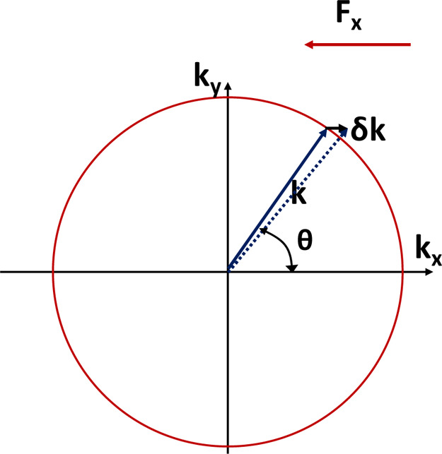
Electron dynamics in the presence of optical field F.
The projection of the velocity of this electron onto the direction of field is
| 10 |
Taking derivative, we obtain
| 11 |
Therefore, the velocity of the electron in the presence of dc field is
| 12 |
Now, one can obtain the expression for the current density as
| 13 |
where gV = 2 is the valley degeneracy, which yields precisely eq 6 for the sheet conductivity. Now, if we average eq 12 over the angle θ, we can write
| 14 |
where the energy-dependent mobility is
| 15 |
and
| 16 |
where f(k) is the distribution function. Herein lies the physical origin of the strength of the bolometric effect in graphene—the extreme non-parabolicity of the dispersion. If the dispersion had been parabolic, then the square of velocity in eq 15 would have been proportional to energy as mcv2/2 = E, where mc is effective mass, which would have made mobility-independent of energy, μ = eτm/mc.
Therefore, when the i-th electron gets promoted from state 1i to state 2i (leaving a hole in state 1i behind) because of heating, its mobility gets reduced by
| 17 |
All that is left is to calculate the total bolometric change of sheet conductivity by summing up individual electron–hole pair contributions eq 17 within unit area according to eq 16 and use eq 8
| 18 |
From eq 6, we can express e2τm = σπh2/EF, and therefore, relative bolometric change is
| 19 |
The change in resistance can then be simply estimated by averaging eq 19 as
| 20 |
where W and L1 are the width and the length of graphene, respectively, that absorb a light and ηabs is the absorption efficiency. Note that if the doping is electrostatic, then the total charge in the graphene can be found as roughly enWL = Cg(Vg – Vt), where Cg is gate capacitance and Vt is threshold voltage and then
| 21 |
Comparison of Two Effects
Before continuing, we need to develop the expression for the hole conductivity for the case of low carrier concentration, when the Fermi energy is comparable or less than kBT or δp < Neff = (2/π) (kBT/hvF)2 ≈ 1010 cm–2 and the carriers are distributed according to Boltzmann distribution with energy counted down
| 22 |
where EV is the quasi-Fermi level of the valence band and Tp is the temperature of hot holes following excitation, which is, in general photon energy-dependent and can be anywhere from lattice temperature to hω/2kB. We only need a very rough idea about its magnitude in order to show that PC effect is weaker than the bolometric one. Substituting eq 22 into eq 16, we then obtain the expression for the hole photoconductivity
| 23 |
| 24 |
Since δn = δp we obtain
| 25 |
We can now compare photoconductive response with the bolometric one—essentially
| 26 |
This follows from the fact that EF < hω/2, τee < τEL, and the expression in parenthesis is on the order of a few times unity. Hence, bolometric effect dominates.
Bolometric Photodetector Arrangement
To maximize the PB photodetector performances expressed by eqs 20 and 21, we propose a plasmonic bolometric photodetector operating at telecom wavelengths that is based on the long-range dielectric loaded surface plasmon polariton (LR-DLSPP) waveguide49−51 with graphene placed at the maximum electric field of the propagating mode (Figure 3). As a result, the plasmonic mode is highly absorbed by the graphene sheet, enhancing thermally activated carrier transport in the graphene,45 while the absorption losses in metal are highly reduced.
To achieve efficient absorption in graphene, it is necessary to maximize the in-pane component of the electric field. The in-plane electric field component of the propagating LR-DLSPP mode interacts strongly with graphene enhancing absorption (Figure 4). The presence of the in-plane component of the electric field even for the TM mode is associated here with the small thickness of the metal stripe and its sharp metal corners.31 The electric field at the metal stripe’s corners is very strong but decays quickly on the graphene. This produces hot carriers in very close proximity to the metal stripe.
Figure 4.

(a) In-plane electric field component of the plasmonic TM mode on graphene surface with a corresponding (b) electric field profile (Ey) for the cross section of the photodetector as presented in (c). The E2 of the mode is presented in (d).
To minimize the contribution from the PTE effect that requires an asymmetric electron distribution in a graphene channel,13,16,33 the symmetric contact arrangement has been implemented here, that is, the same metals were used as contacts and the structure was symmetric with respect to the center of the metal stripe/ridge (Figure 3). As a result, a symmetric band diagram across the active graphene channel is achieved. Consequently, only the aforementioned PB and PC effects can exist under this arrangement and, as has been shown above, PC effect is invariably weaker than a bolometric one.
Electron–Electron and Electron-Phonon Scattering times
The theory of hot-carrier induced bolometric effect presented in previous sections relies on the fact that carriers inside the graphene stay out of equilibrium with lattice for a relatively long time τel52−54 that is longer than the time that it takes to establish the thermalized distribution among the electrons—τee.55−57 Here, we preset estimates of these rates and compare them with available experimental data. The e–e scattering rate, under large doping of graphene, when the Fermi energy EF exceeds kBTe, the inelastic scattering rate tends to form
| 27 |
Here, Te is the electron temperature in graphene and α is defined as58
| 28 |
where εr is the dielectric constant. In the next step, the energy from the electrons is dissipated (relaxed) either by the energy transfer to the lattice via the e–l coupling or by electron diffusion away from the heated region33,48,59 (Figure 5). The e–l scattering rate is defined as60
| 29 |
where D = 18 eV is the deformation potential, ρm = 7.4 × 10⁻⁷ kg/m2 is the mass density of monolayer graphene,39,61vs = 2.6 × 10⁴ m/s is the phonon velocity in graphene, Ek is the carrier energy, and TL is the lattice temperature.
Figure 5.

Electron temperature-dependent e–e and e–l scattering times for different lattice temperatures TL = 293 K (red and blue curves) and TL = 600 K (black curve). The ambient (room) temperature was assumed at T0 = 293 K.
In graphene, the Fermi energy is much smaller than in conventional metals; thus, the e–e scattering time is extremely fast even is the doped regime with the smallest value achieved near the Dirac point.58 In comparison, the e–l scattering time is much slower than e–e scattering time and range from 1 to 2 ps under the room temperature operation conditions.33,36,48,52,55,56 However, for higher lattice temperature TL, the e–l scattering time decreases52,57 (Figure 5). From the scattering rates, it can be concluded that an increase of phonon/lattice temperature TL leads to increased e–l scattering rate, that is, decreased e–l scattering time and, in consequence, a reduction in transport current, that is, decrease of ΔR/R, while an increase in electron temperature Te is equivalent to an increased carrier density and leads to an increase in transport current. The increase of the lattice temperature TL leads to a more efficient cooling pathway for hot electrons54 because additional phonons become available for heat dissipation.25,26,55,62 The lattice temperature can be increased in the graphene either through a Joule heating that is proportional to the applied electrical power25,55,62 or through highly confined plasmonic energy.26 Thus, for compact devices, where the (electrical) power density is high, the increases of TL can provide additional heat dissipation channel, in consequence, reducing a PB effect.32 Simultaneously, as it has been previously observed that55 the efficiency of electron heating is independent of lattice temperature and depends only on the in-plane component of the electric field coupled to the graphene.
Evaluation of PB Photodetector Performances
Having estimated the scattering times, we can evaluate the detector performance. For a large distance of hot electrons to external electrodes exceeding the electron mean free path lMFP, the main heat-flow channel of hot electrons is through relaxation to the graphene lattice. In such a case, the ratio of resistance ΔR/R is very valuable formula to evaluate a bolometric photodetector. The ratio of resistance ΔR/R is calculated from eq 20, and results are showed in Figure 6 with W = 40 μm and L1 = 10 nm. As observed from Figure 6, the maximum resistance ratio was calculated at ΔR/R = 23 for EF = 0.1 eV. When compared with other plasmonic PB photodetectors,12 the resistance ratio was much smaller calculated at ΔR/R = 7.7 for EF = 0.1 eV.
Figure 6.
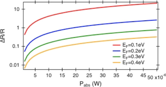
Ratio of resistances as a function of absorbed power by the graphene sheet for different Fermi energies EF and carrier concentrations n. Here, the lattice temperature was kept at the ambient temperature, that is, TL = T0 = 293 K.
To evaluate ΔR/R, the power absorbed by the graphene should be calculated. The power absorbed by the graphene photodetector Pabs is related to the input power Pin as Pabs = ηabsηcPin, where ηc and ηabs are the coupling and absorption efficiencies, respectively. Here, L1 is the length of the in-plane electric field interacting with graphene. The coupling efficiency in this type of plasmonic waveguide can exceed 90%, with absorption efficiency exceeding 40% for 40 μm-long and up to 63% for 100 μm-long photodetectors, respectively (Figure 7) (Methods section). Simultaneously, as shown in Figure 4a, the power is absorbed by less than 10 nm-wide graphene. As a result, the power absorbed by the graphene is extremely high, enhancing the electron temperature in the graphene.
Figure 7.

Comparison of the light absorption efficiencies in graphene for the LR-DLSPP-based photodetector and the MIM-based photodetector proposed here.32
Under zero bias voltage, the PB photocurrent does not exist. However, under a bias voltage applied across the metallic contact, the change of graphene resistance can be detected by the change of the photocurrent flowing through the graphene sheet as
| 30 |
Thus, the responsivity of photodetector is expressed by
| 31 |
Consequently, knowing the photocurrent of the photodetector and input power, the responsivity can be calculated. The calculations were performed for conductivity σ0 = 0.4 mS, similar to ref (12). For L = 800 nm long and W = 40 μm wide photodetector, the resistance was calculated at R = 50 Ω. Thus, by the applying a bias voltage of 1 V, a current I = 20 mA at room temperature T0 = 293 K was calculated. As observed from Figure 6 (ratio of resistances), the PB photodetector works in an inverse operation mode with the off-state in the dark (where the current signal is high) and the on-state with light incidence (where the current signal is low). Furthermore, to achieve a large on–off state, a strong suppression of the current is highly desired with an applied optical signal. This observation is consistent with experimental work performed with the bow-tie PB photodetector.12 The current change between off and on state corresponds to a photocurrent (eq 30).
When light is delivered to the photodetector with an input power of 50 μW that corresponds to the absorbed power of 20 μW, the external responsivity was calculated at Rph = 150 A/W and Rph = 120 A/W for Fermi energies of 0.1, and 0.2 eV (Figure 8a). For lower input power of 5 μW, that is, absorbed power Pabs = 2 μW, the external responsivity was calculated at Rph = 1100 A/W for EF = 0.1 eV, while for EF = 0.2 eV, it was calculated at Rph = 350 A/W (Figure 8a). As observed from above, the low power operation is desired for the best performance of the PB photodetector as it reduces power requirements and ensures it enhances responsivity for all Fermi energies studied here.
Figure 8.

(a) Responsivity as a function of input power Pin for different Fermi energies and (b) normalized current responsivity as a function of Fermi energy EF.
Another very valuable parameter that characterizes the performance of the photodetectors is the normalized current responsivity (in %/W) defined as63
| 32 |
where ION is the current without illumination and Pin is the input power. For ΔR/R ≈ 10 at EF = 0.1 eV and for Pabs = 20 μW absorbed power (Figure 6), that corresponds to the input power of 50 μW, the normalized current responsivity was calculated at Rph,N = 1.9·107%/W (Figure 8b). It is three orders of magnitude higher than state-of-the-art pyroelectric bolometer based on graphene–lithium niobate (LN), Rph,N = 2·104%/W,63 and five orders of magnitude higher than the pyroelectric bolometer based on a graphene–lead zirconate titanate, Rph,N = 1.2 × 10²%/W.64 However, despite of a comparable responsivity of the graphene–LN photodetector, the operation speed is limited to 1 kHz what makes it inefficient for high speed operations.
In graphene hot electron photodetectors such as PB photodetectors, the response time and thus the bandwidth of the photodetector are determined by the e–l relaxation time that is required for graphene devices to return to equilibrium.10,25,26,33,54 As previously experimentally observed25,26,33,52,54,57,65 and confirmed by calculations performed here, the e–l relaxation time range from hundreds of femtoseconds to tens of picoseconds that depends on the carrier concentration in graphene as well as the lattice and electron temperatures. As a consequence, graphene hot electron bolometers enable a realization of photodetectors with the bandwidth approaching 500 GHz. As it has been previously shown, the bandwidth of the PB photodetector can exceed 110 GHz12 and is only limited by the product of the electronic heat capacitance and thermal resistance.12
Conclusions
Here, a theory of the bolometric effect originating from the band nonparabolicity of graphene was developed, and new waveguide-integrated plasmonic graphene bolometer was proposed with the ratio of resistances exceeding 23. As such, the responsivity exceeding 1100 A/W is expected to be attained. The extremely fast response time of hot carriers in graphene enables a realization of photodetectors with response well beyond hundreds of GHz. The improved performances originate from the highly localized in-plane component of the electric field that is mostly absorbed within 10 nm from a metal stripe. The results show the potential of graphene for high-speed communication systems.
Methods
Estimation of Power Absorbed by a Graphene Sheet
To evaluate the performance of the proposed photodetector, the amount of power absorbed by a graphene sheet need to be determined. Power absorbed by the graphene sheet can be calculated as follow
| 33 |
Here, we simulate around Pin = 50 μW of power coupling to a photodetector that consists of Si as semiconductor ridge and semiconductor buffer and Au as metal stripe (Figures 3 and 4). The Si ridge (semiconductor ridge) width and thickness were taken at 380 and 210 nm, respectively, while Si rib thickness (semiconductor buffer) was taken at 90 nm. The Au stripe width was taken at 80 nm and thickness at 12 nm, while a distance between external electrodes (metal pad 1 and metal pad 2) was taken at 800 nm.
For the absorption coefficient of graphene αG and metal αM obtained from a simulation, the length-dependent of fraction of light absorption in graphene ηabs can be calculated by
| 34 |
where L is the length of photodetector. Calculations were performed for a telecom wavelength of 1550 nm, and results were summarized in Figure 7. From this figure, it can be deduced that for a 40 μm-long photodetector, about 40% of the power is absorbed by graphene (Figure 7). As a result, we can assume that a power of Pabs = 20 μW absorbed by graphene will contribute to a photocurrent generation.
Acknowledgments
The support of a National Science Foundation grant no. 1507749 is gratefully acknowledged.
Author Contributions
J.G. conceived the idea of detector, performed all calculations and FEM and FDTD simulations and wrote the article. J.B.K. derived the analytical estimate of bolometric and PC responses. J.G. and J.B.K. analyzed and discussed the results. Both authors reviewed the article.
The authors declare no competing financial interest.
References
- Thomson D.; Zilkie A.; Bowers J. E.; Komljenovic T.; Reed G. T.; Vivien L.; Marris-Morini D.; Cassan E.; Virot L.; Fédéli J.-M.; Hartmann J.-M.; Schmid J. H.; Xu D.-X.; Boeuf F.; O’Brien P.; Mashanovich G. Z.; Nedeljkovic M. Roadmap on silicon photonics. J. Optic. 2016, 18, 073003. 10.1088/2040-8978/18/7/073003. [DOI] [Google Scholar]
- Piels M.; Bowers J. E.. Photodetectors for silicon photonic integrated circuits. In Photodetectors; Nabet B., Ed.; Woodhead Publishing, 2018; pp 3–20. [Google Scholar]
- Miller D. A. B. Attojoule optoelectronics for low-energy information processing and communications. J. Lightwave Technol. 2017, 35, 346–396. 10.1109/jlt.2017.2647779. [DOI] [Google Scholar]
- Amin R.; Zhizhen M.; Maiti R.; Miscuglio M.; Dalir H.; Khurgin J. B.; Sorger V. J.. A Guide for Material and Design Choices for Electro-Optic Modulators and recent 2D-Material Silicon Modulator Demonstrations. 2018, arXiv.org 2018, arXiv:1812.11096. [Google Scholar]
- Romagnoli M.; Sorianello V.; Midrio M.; Koppens F. H. L.; Huyghebaert C.; Neumaier D.; Galli P.; Templ W.; D’Errico A.; Ferrari A. C. Graphene- based integrated photonics for next- generation datacom and telecom. Nat. Rev. Mater. 2018, 3, 392–414. 10.1038/s41578-018-0040-9. [DOI] [Google Scholar]
- Koppens F. H. L.; Mueller T.; Avouris P.; Ferrari A. C.; Vitiello M. S.; Polini M. Photodetectors based on graphene, other two-dimensional materials and hybrid systems. Nat. Nanotechnol. 2014, 9, 780–793. 10.1038/nnano.2014.215. [DOI] [PubMed] [Google Scholar]
- Leuthold J.; Hoessbacher C.; Muehlbrandt S.; Melikyan A.; Kohl M.; Koos C.; Freude W.; Dolores-Calzadilla V.; Smit M.; Suarez I.; Martínez-Pastor J.; Fitrakis E. P.; Tomkos I. Plasmonic Communications: Light on a Wire. Optic Photon. J. 2013, 24, 28–35. 10.1364/opn.24.5.000028. [DOI] [Google Scholar]
- Khurgin J. B. Relative merits of phononics vs. plasmonics: the energy balance approach. Nanophotonics 2018, 7, 305–316. 10.1515/nanoph-2017-0048. [DOI] [Google Scholar]
- Schuller J. A.; Barnard E. S.; Cai W.; Jun Y. C.; White J. S.; Brongersma M. L. Plasmonics for extreme light concentration and manipulation. Nat. Mater. 2010, 9, 193–204. 10.1038/nmat2630. [DOI] [PubMed] [Google Scholar]
- Yao Y.; Shankar R.; Rauter P.; Song Y.; Kong J.; Loncar M.; Capasso F. High-Responsivity Mid-Infrared Graphene Detectors with Antenna-Enhanced Photocarrier Generation and Collection. Nano Lett. 2014, 14, 3749–3754. 10.1021/nl500602n. [DOI] [PubMed] [Google Scholar]
- Ding Y.; Cheng Z.; Zhu X.; Yvind K.; Dong J.; Galili M.; Hu H.; Mortensen N. A.; Xiao S.; Oxenløwe L. K.. Ultra-compact integrated graphene plasmonic photodetector with bandwidth above 110 GHz. Nanophotonics 2020, 9, doi: 10.1515/nanoph-2019-0167. [DOI] [Google Scholar]
- Ma P.; Salamin Y.; Baeuerle B.; Josten A.; Heni W.; Emboras A.; Leuthold J. Plasmonically Enhanced Graphene Photodetector Featuring 100 Gbit/s Data Reception, High Responsivity, and Compact Size. ACS Photonics 2019, 6, 154–161. 10.1021/acsphotonics.8b01234. [DOI] [Google Scholar]
- Gosciniak J.; Rasras M.; Khurgin J. B. Ultrafast Plasmonic Graphene Photodetector Based on the Channel Photothermoelectric Effect. ACS Photonics 2020, 7, 488–498. 10.1021/acsphotonics.9b01585. [DOI] [Google Scholar]
- Muehlbrandt S.; Melikyan A.; Harter T.; Köhnle K.; Muslija A.; Vincze P.; Wolf S.; Jakobs P.; Fedoryshyn Y.; Freude W.; Leuthold J.; Koos C.; Kohl M. Silicon-plasmonic internal-photoemission detector for 40 Gbit/s data reception. Optica 2016, 3, 741–747. 10.1364/optica.3.000741. [DOI] [Google Scholar]
- Goykhman I.; Sassi U.; Desiatov B.; Mazurski N.; Milana S.; de Fazio D.; Eiden A.; Khurgin J.; Shappir J.; Levy U.; Ferrari A. C. On-chip integrated, silicon–graphene plasmonic Schottky photodetector with high responsivity and avalanche photogain. Nano Lett. 2016, 16, 3005–3013. 10.1021/acs.nanolett.5b05216. [DOI] [PMC free article] [PubMed] [Google Scholar]
- Muench J. E.; Ruocco A.; Giambra M. A.; Miseikis V.; Zhang D.; Wang J.; Watson H. F. Y.; Park G. C.; Akhavan S.; Sorianello V.; Midrio M.; Tomadin A.; Coletti C.; Romagnoli M.; Ferrari A. C.; Goykhman I. Waveguide-integrated, plasmonic enhanced graphene photodetectors. Nano Lett. 2019, 19, 7632–7644. 10.1021/acs.nanolett.9b02238. [DOI] [PubMed] [Google Scholar]
- Gosciniak J.; Atar F. B.; Corbett B.; Rasras M. Plasmonic Schottky photodetector with metal stripe embedded into semiconductor and with a CMOS-compatible titanium nitride. Sci. Rep. 2019, 9, 6048. 10.1038/s41598-019-42663-3. [DOI] [PMC free article] [PubMed] [Google Scholar]
- Gosciniak J.; Atar F. B.; Corbett B.; Rasras M. CMOS-Compatible Titanium Nitride for On-Chip Plasmonic Schottky Photodetectors. ACS Omega 2019, 4, 17223–17229. 10.1021/acsomega.9b01705. [DOI] [PMC free article] [PubMed] [Google Scholar]
- Gosciniak J.; Rasras M. High-bandwidth and high-responsivity waveguide-integrated plasmonic germanium photodetector. J. Opt. Soc. Am. B 2019, 36, 2481–2491. 10.1364/josab.36.002481. [DOI] [Google Scholar]
- Salamin Y.; Ma P.; Baeuerle B.; Emboras A.; Fedoryshyn Y.; Heni W.; Cheng B.; Josten A.; Leuthold J. 100 GHz Plasmonic Photodetector. ACS Photonics 2018, 5, 3291–3297. 10.1021/acsphotonics.8b00525. [DOI] [Google Scholar]
- Geim A. K.; Novoselov K. S. The rise of graphene. Nat. Mater. 2007, 6, 183–191. 10.1038/nmat1849. [DOI] [PubMed] [Google Scholar]
- Bonaccorso F.; Sun Z.; Hasan T.; Ferrari A. C. Graphene photonics and optoelectronics. Nat. Photonics 2010, 4, 611–622. 10.1038/nphoton.2010.186. [DOI] [Google Scholar]
- Castro Neto A. H.; Guinea F.; Peres N. M. R.; Novoselov K. S.; Geim A. K. The electronic properties of graphene. Rev. Mod. Phys. 2009, 81, 109–162. 10.1103/revmodphys.81.109. [DOI] [Google Scholar]
- Dorodnyy A.; Salamin Y.; Ma P.; Vukajlovic Plestina J.; Lassaline N.; Mikulik D.; Romero-Gomez P.; Fontcuberta I Morral A.; Leuthold J. Plasmonic Photodetectors. IEEE J. Sel. Top. Quantum Electron. 2019, 24, 4600313. 10.1016/b978-1-78242-445-1.00006-3. [DOI] [Google Scholar]
- Freitag M.; Low T.; Xia F.; Avouris P. Photoconductivity of biased graphene. Nat. Photonics 2013, 7, 53–59. 10.1038/nphoton.2012.314. [DOI] [Google Scholar]
- Freitag M.; Low T.; Zhu W.; Yan H.; Xia F.; Avouris P. Photocurrent in graphene harnesses by tunable intrinsic plasmons. Nat. Commun. 2013, 4, 1951. 10.1038/ncomms2951. [DOI] [PubMed] [Google Scholar]
- Grigorenko A. N.; Polini M.; Novoselov K. S. Graphene plasmonics. Nat. Photonics 2012, 6, 749–758. 10.1038/nphoton.2012.262. [DOI] [Google Scholar]
- Liu M.; Yin X.; Ulin-Avila E.; Geng B.; Zentgraf T.; Ju L.; Wang F.; Zhang X. A graphene-based broadband optical modulator. Nature 2011, 474, 64–67. 10.1038/nature10067. [DOI] [PubMed] [Google Scholar]
- Ayata M.; Fedoryshyn Y.; Heni W.; Baeuerle B.; Josten A.; Zahner M.; Koch U.; Salamin Y.; Hoessbacher C.; Haffner C.; Elder D. L.; Dalton L. R.; Leuthold J. High-speed plasmonic modulator in a single metal layer. Science 2017, 358, 630–632. 10.1126/science.aan5953. [DOI] [PubMed] [Google Scholar]
- Gosciniak J.; Tan D. T. H. Theoretical investigation of graphene-based photonic modulators. Sci. Rep. 2013, 3, 1897. 10.1038/srep01897. [DOI] [PMC free article] [PubMed] [Google Scholar]
- Ansell D.; Radko I. P.; Han Z.; Rodriguez F. J.; Bozhevolnyi S. I.; Grigorenko A. N. Hybrid graphene plasmonic waveguide modulators. Nat. Commun. 2015, 6, 8846. 10.1038/ncomms9846. [DOI] [PMC free article] [PubMed] [Google Scholar]
- Ma Z.; Kikunaga K.; Wang H.; Sun S.; Amin R.; Maiti R.; Tahersima M. H.; Dalir H.; Miscuglio M.; Sorger V. J. Compact Graphene Plasmonic Slot Photodetector on Silicon-on-insulator with High Responsivity. ACS Photonics 2020, 7, 932–940. 10.1021/acsphotonics.9b01452. [DOI] [Google Scholar]
- Shautsova V.; Sidiropoulos T.; Xiao X.; Gusken N. A.; Black N. C. G.; Gilbertson A. M.; Giannini V.; Maier S. A.; Cohen L. F.; Oulton R. F. Plasmon induced thermoelectric effect in graphene. Nat. Commun. 2018, 9, 5190. 10.1038/s41467-018-07508-z. [DOI] [PMC free article] [PubMed] [Google Scholar]
- Xia F.; Mueller T.; Lin Y.-m.; Valdes-Garcia A.; Avouris P. Ultrafast graphene photodetector. Nat. Nanotechnol. 2009, 4, 839–843. 10.1038/nnano.2009.292. [DOI] [PubMed] [Google Scholar]
- Luo F.; Zhu M.; Tan Y.; Sun H.; Luo W.; Peng G.; Zhu Z.; Zhang X.-A.; Qin S. High responsivity graphene photodetectors from visible to near-infrared by photogating effect. AIP Adv. 2018, 8, 115106. 10.1063/1.5054760. [DOI] [Google Scholar]
- Urich A.; Unterrainer K.; Mueller T. Intrinsic Response Time of Graphene Photodetectors. Nano Lett. 2011, 11, 2804–2808. 10.1021/nl2011388. [DOI] [PMC free article] [PubMed] [Google Scholar]
- Du X.; Prober D. E.; Vora H.; McKitterick Ch. B. Graphene-based Bolometers. Graphene 2D Mater. 2014, 1, 1–22. 10.2478/gpe-2014-0001. [DOI] [Google Scholar]
- Yan J.; Kim M.-H.; Elle J. A.; Sushkov A. B.; Jenkins G. S.; Milchberg H. M.; Fuhrer M. S.; Drew H. D. Dual-gated bilayer graphene hot-electron bolometer. Nat. Nanotechnol. 2012, 7, 472–478. 10.1038/nnano.2012.88. [DOI] [PubMed] [Google Scholar]
- Walsh E. D.; Efetov D. K.; Lee G.-H.; Heuck M.; Crossno J.; Ohki T. A.; Kim P.; Englund D.; Fong K. Ch. Graphene-Based Josephson-Junction Single-Photon Detector. Appl. Phys. Rev. 2017, 8, 024022. 10.1103/physrevapplied.8.024022. [DOI] [Google Scholar]
- Efetov D. K.; Shiue R.-J.; Gao Y.; Skinner B.; Walsh E. D.; Choi H.; Zheng J.; Tan C.; Grosso G.; Peng C.; Hone J.; Fong K. C.; Englund D. Fast thermal relaxation in cavity-coupled graphene bolometers with a Johnson noise read-out. Nat. Nanotechnol. 2018, 13, 797–801. 10.1038/s41565-018-0169-0. [DOI] [PubMed] [Google Scholar]
- Ryzhii V.; Ryzhii M.; Ponomarev D. S.; Leiman V. G.; Mitin V.; Shur M. S.; Otsuji T. Negative photoconductivity and hot-carrier bolometric detection of terahertz radiation in graphene-phosophorene hybrid structures. J. Appl. Phys. 2019, 125, 151608. 10.1063/1.5054142. [DOI] [Google Scholar]
- Rogalski A.Infrared Detectors; CRC Press, 2011. [Google Scholar]
- Shao Q.; Liu G.; Teweldebrhan D.; Balandin A. A. High-temperature quenching of electrical resistance in graphene interconnects. Appl. Phys. Lett. 2008, 92, 202108. 10.1063/1.2927371. [DOI] [Google Scholar]
- Yadav A. K.; Khan S. M.; Kundu A.; Rani R.; Soin N.; McLaughlin J.; Misra D. S.; Hazra K. S. Vertically Aligned Few-Layered Graphene-Based Non-Cryogenic Bolometer. C J. of Carbon Research 2019, 5, 23. 10.3390/c5020023. [DOI] [Google Scholar]
- Guo Q.; Yu R.; Li C.; Yuan S.; Deng B.; de Abajo F. J. G.; Xia F. Efficient electrical detection of mid-infrared graphene plasmons at room temperature. Nat. Mater. 2018, 17, 986–992. 10.1038/s41563-018-0157-7. [DOI] [PubMed] [Google Scholar]
- McKitterick C. B.; Prober D. E.; Karasik B. S. Performance of graphene thermal photon detectors. J. Appl. Phys. 2013, 113, 044512. 10.1063/1.4789360. [DOI] [Google Scholar]
- Efetov D.; Kim P. Controlling electron-phonon interactions in graphene at ultrahigh carrier densities. Phys. Rev. Lett. 2010, 105, 256805. 10.1103/physrevlett.105.256805. [DOI] [PubMed] [Google Scholar]
- Brida D.; Tomadin A.; Manzoni C.; Kim Y. J.; Lombardo A.; Milana S.; Nair R. R.; Novoselov K. S.; Ferrari A. C.; Cerullo G.; Polini M. Ultrafast collinear scattering and carrier multiplication in graphene. Nat. Commun. 2013, 4, 1987. 10.1038/ncomms2987. [DOI] [PubMed] [Google Scholar]
- Holmgaard T.; Gosciniak J.; Bozhevolnyi S. I. Long-range dielectric-loaded surface plasmon polariton waveguides. Opt. Mater. Express 2010, 18, 23009–23015. 10.1364/oe.18.023009. [DOI] [PubMed] [Google Scholar]
- Gosciniak J.; Holmgaard T.; Bozhevolnyi S. I. Theoretical analysis of long-range dielectric-loaded surface plasmon polariton waveguides. J. Lightwave Technol. 2011, 29, 1473–1481. 10.1109/jlt.2011.2134071. [DOI] [Google Scholar]
- Volkov V. S.; Han Z.; Nielsen M. G.; Leosson K.; Keshmiri H.; Gosciniak J.; Albrektsen O.; Bozhevolnyi S. I. Long-range dielectric-loaded surface plasmon polariton waveguides operating at telecommunication wavelengths. Opt. Lett. 2011, 36, 4278–4280. 10.1364/ol.36.004278. [DOI] [PubMed] [Google Scholar]
- Song J. C. W.; Levitov L. S. Energy Flows in Graphene: Hot Carrier Dynamics and Cooling. J. Phys. Condens. Matter 2015, 27, 164201. 10.1088/0953-8984/27/16/164201. [DOI] [PubMed] [Google Scholar]
- Ma Q.; Gabor N. M.; Andersen T. I.; Nair N. L.; Watanabe K.; Taniguchi T.; Jarillo-Herrero P. Competing Channels for Hot-Electron Cooling in Graphene. Phys. Rev. Lett. 2014, 112, 247401. 10.1103/physrevlett.112.247401. [DOI] [PubMed] [Google Scholar]
- Graham M. W.; Shi S.-F.; Ralph D. C.; Park J.; McEuen P. L. Photocurrent measurements of supercollision cooling in graphene. Nat. Phys. 2013, 9, 103–108. 10.1038/nphys2493. [DOI] [Google Scholar]
- Tielrooij K. J.; Piatkowski L.; Massicotte M.; Woessner A.; Ma Q.; Lee Y.; Myhro K. S.; Lau C. N.; Jarillo-Herrero P.; van Hulst N. F.; Koppens F. H. L. Generation of photovoltage in graphene on a femtosecond timescale through efficient carrier heating. Nat. Nanotechnol. 2015, 10, 437–443. 10.1038/nnano.2015.54. [DOI] [PubMed] [Google Scholar]
- Chen Y.; Li Y.; Zhao Y.; Zhou H.; Zhu H. Highly efficient hot electron harvesting from graphene before electron-hole thermalization. Sci. Adv. 2019, 5, eaax9958 10.1126/sciadv.aax9958. [DOI] [PMC free article] [PubMed] [Google Scholar]
- Song J. C. W.; Rudner M. S.; Marcus C. M.; Levitov L. S. Hot Carrier Transport and Photocurrent Response in Graphene. Nano Lett. 2011, 11, 4688–4692. 10.1021/nl202318u. [DOI] [PubMed] [Google Scholar]
- Lucas A.; Fong K. C. Hydrodynamics of electrons in graphene. J. Phys.: Condens. Matter 2018, 30, 053001. 10.1088/1361-648x/aaa274. [DOI] [PubMed] [Google Scholar]
- Lin Y.; Ma Q.; Shen P.-C.; Ilyas B.; Bie Y.; Liao A.; Ergeçen E.; Han B.; Mao N.; Zhang X.; Ji X.; Zhang Y.; Yin J.; Huang S.; Dresselhaus M.; Gedik N.; Jarillo-Herrero P.; Ling X.; Kong J.; Palacios T. Asymmetric hot-carrier thermalization and broadband photoresponse in graphene-2D semiconductor lateral hererojunctions. Sci. Adv. 2019, 5, eaav1493 10.1126/sciadv.aav1493. [DOI] [PMC free article] [PubMed] [Google Scholar]
- Ge Y.; Fisher T. S.. First-principles prediction of bilayer graphene photoconductivity. 2019, arXiv.org 2019, arXiv:1907.11323. [Google Scholar]
- Viljas J. K.; Heikkila T. T. Electron-phonon heat transfer in monolayer and bilayer graphene. Phys. Rev. B: Condens. Matter Mater. Phys. 2010, 81, 245404. 10.1103/physrevb.81.245404. [DOI] [Google Scholar]
- Zhu W.; Perebeinos V.; Freitag M.; Avouris P. Carrier scattering, mobilities, and electrostatic potential in monolayer, bilayer, and trilayer graphene. Phys. Rev. B: Condens. Matter Mater. Phys. 2009, 80, 235402. 10.1103/physrevb.80.235402. [DOI] [Google Scholar]
- Sassi U.; Parret R.; Nanot S.; Bruna M.; Borini S.; De Fazio D.; Zhao Z.; Lidorikis E.; Koppens F. H. L.; Ferrari A. C.; Colli A. Graphene-based mid-infrared room-temperature pyroelectric bolometers with ultrahigh temperature coefficient of resistance. Nat. Commun. 2017, 8, 14311. 10.1038/ncomms14311. [DOI] [PMC free article] [PubMed] [Google Scholar]
- Hsieh C.-Y.; Chen Y.-T.; Tan W.-J.; Chen Y.-F.; Shih W. Y.; Shih W.-H. Graphene-lead zirconate titanate optothermal field effect transistors. Appl. Phys. Lett. 2012, 100, 113507. 10.1063/1.3693607. [DOI] [Google Scholar]
- Tielrooij K. J.; Song J. C. W.; Jensen S. A.; Centeno A.; Pesquera A.; Zurutuza Elorza A.; Bonn M.; Levitov L. S.; Koppens F. H. L. Photoexcitation cascade and multiple hot-carrier generation in graphene. Nat. Phys. 2013, 9, 248–252. 10.1038/nphys2564. [DOI] [Google Scholar]
- Guo J.; Li J.; Liu Ch.; Yin Y.; Wang W.; Ni Z.; Fu Z.; Yu H.; Xu Y.; Shi Y.; Ma Y.; Gao S.; Tong L.; Dai D. High-performance silicon-graphene hubrid plasmonic waveguide photodetectors beyond 1.55 um. Light: Sci. Appl. 2020, 9, 9–29. 10.1038/s41377-020-0263-6. [DOI] [PMC free article] [PubMed] [Google Scholar]