Abstract
In this paper, a wide bandwidth angle- and polarization-insensitive symmetric metamaterial (MM) absorber for X and Ku band is proposed. For both normal and oblique incidence in TEM mode, the proposed unit cell shows high absorption at different polarizing angles due to structural symmetry. A four-fold resonator was introduced in the unit cell to enhance the bandwidth. The performance of the proposed absorber is determined by both full-wave simulations and measurements. The simulated and measured absorptions are almost similar at normal incidence with 94.63%, 95.58%, 97% and 75.58% at 11.31 GHz, 14.11 GHz, 14.23 GHz, and 17.79 GHz respectively. At 45° for these frequencies, the absorptions are 95.47%, 97.2%, 97.12% and 75.29% respectively. For 90°, the absorptions are similar to those for 45° except 98.15% for 14.21 GHz. At all these angles and resonance frequencies, either permittivity or permeability was found negative, as a result, the refractive index was negative revealing metamaterial characteristics of the unit cell. Along with high absorptivity and wide incidence angle insensitivity up to 90°, a total of 1.42 GHz of absorption bandwidth was achieved, which is better than recent similar works with FR4 substrate.
Subject terms: Engineering, Physics
Introduction
Metamaterial (MM) absorbers are recent developments in the field of electromagnetic wave applications like 5 G antenna, Radar cross-section reduction, remote sensing, stealth technology and photo-electron absorption in THz range, etc. MM absorbers are those materials that usually exhibit either negative permittivity or negative permeability or both are negative when electromagnetic (EM) waves pass through them1–3. As a result, they absorb most of the EM waves, as the transmission coefficient of MM absorber is negligible, and the reflection coefficient is very small. These properties are not present in any material generally used for EM wave applications unless they are engineered4,5. Research is going on to achieve absorbance of certain selective range or entire incident EM waves for purpose-wise applications6–10. Different types of substrate materials are used for appropriate di-electric properties for the desired absorbance of the EM waves11. FR4 (fire retardant 4) is one of the most popular and widely used substrates for MM absorber design12. Although FR4 is not appropriate because of high dielectric loss13 at high-frequency range like X and Ku band, it is popular because of low cost, availability and most importantly, absorber applications due to high dielectric loss.
The absorption capability of an MM absorber depends not only on the unit cell design but also on the angle of incidence of the incident EM wave and their polarization types. EM waves are sometimes needed to be absorbed for sensing devices or frequency-selective antenna where the type of polarization and incident angle is important for the absorption capacity of the absorber.
Research is going on to design MM absorbers with features like angle and polarization insensitiveness. The unit cell should also be symmetrically shaped like a split-ring cross resonator, circular sector, Jerusalem cross-section, four-fold symmetric and so on14–19. These absorbers can absorb EM waves with high efficiency at some certain frequencies with very low bandwidth. Hence, they are not appropriate for mass deployment into places for wide bandwidth absorption like radar cross-section reduction, remote sensing, unwanted frequency absorption in antennae, stealth capability in modern military airplanes and so on. To overcome all these challenges in this modern age, the MM absorbers should be designed with such precision that, they will be polarization and wide-angle insensitive, symmetric in structural design, capable of high absorption and most importantly, they must have broad bandwidth of absorption efficiency. For both X and Ku band, only a few absorbers are designed with FR4 to date. The efficiency of those absorbers is not at a satisfactory level concerning the afore-mentioned performance indicators.
In this paper, we propose an MM absorber which satisfies all these properties for X and Ku band applications. We also have compared the performance of the unit cell with recently published relevant absorbers and found it better in all aspects of the above-mentioned performance categories. The most popular FR4 substrate is used as the dielectric barrier for the unit cell, where the copper patch is backed up by a copper ground with the substrate in between them.
Design of unit cell
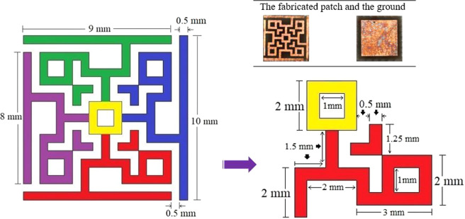
Usually, absorption with broad bandwidth and negative value of either permittivity or permeability or both, are the key objectives of designing an MM absorber. Any substrate can be used to design the patch on it with or without a ground at the opposite side of the patch. Commercially and widely used FR4 is not found much with broad bandwidth absorption in the X and Ku band regions. In this project, FR4 substrate (loss tangent = 0.025, dielectric constant = 4.3 and relative permeability = 1) with 1.578 mm thickness was used to design the proposed MM absorber unit cell. Fortunately, a broadband frequency absorption was achieved with so many attempts in the patch and the ground plane design with ending up to the following design shown in Fig. 1. The shape of the patch became like this from the intention of keeping square-shaped inductive and rectangular-shaped capacitive ring elements with 90-degree symmetric rotations. The metallic square rings are continuous for ensuring inductance and the rectangular rings are discontinuous by splits for capacitance. The entire unit cell is four-fold symmetrical as each quadrant are equivalent and rotated by 90 degrees. The size of the unit cell is 10 × 10 mm. The detailed dimension of the unit cell and a quadrant is shown in Fig. 2. Each quadrant is shown in different colors for the understanding of the patch design with the central square associated with all quadrants.
Figure 1.
Design of the unit cell.
Figure 2.
Dimension of the patch.
Each quadrant acts as an associate resonator to demonstrate the single negative value of either permittivity or permeability. The center of the total patch acts as a bridge to ensure equivocal current flow from any direction throughout the unit cell. The slits at the square border act as a capacitive load to perform for absorption in the lower frequencies (X band), whereas the discontinuities in the body of the patchwork for absorption in the higher frequencies (Ku band). Each quadrant with the center square and the perimeter lines act as inductive loads with complex values for reflection and transmission coefficients. The ground was chosen to reflect EM waves only to the quadrants except for the circumferential border transmission lines for better performance. This was because, the EM waves (any type of polarized) were needed to be rippled back from the ground to the patch so that the transmission coefficient of the unit cell is not negligible, which is essential to ensure negative values of permittivity and permeability.
The unit cell was fabricated (as shown in the top inset of Fig. 2) and data were taken using the cell in the PNA Network analyzer (N5227A).
Metamaterial fundamentals and results
The absorption capability of an MM absorber can be calculated by
| 1 |
if the reflection coefficient R (ω) and transmission coefficient T(ω) are zero, the highest absorption can be achieved. In the case of normal incidence of EM wave, the reflection coefficient can be achieved by
| 2 |
where Z(ω) is the impedance of the MM absorber and zo is the impedance of the free space (air). When Z(ω) = Zo = 377 Ω, the reflection coefficient becomes zero. The characteristic or built-in impedance of the absorber can be found by
| 3 |
as the designed unit cell has a symmetric patch, the dependence of characteristic impedance of the cell on the incident angle was not an issue. Furthermore, the groundsheet at the back of the substrate didn’t allow any EM waves to be transmitted through it. Hence the transmission coefficient was negligible and any amount of it was dissipated due to the dielectric loss tangent of the substrate medium. The simulated values of the reflection (S11) and transmission (S21) coefficients were found below −10dB at the resonance frequencies.
The refractive index (η) of the unit cell was calculated by two different methods: the Nicolson-Ross-Weir (NRW) method and the Direct Refractive Index (DRI) method as shown in the Eqs. (4) and (7) below.
| 4 |
Where,
| 5 |
And
| 6 |
here ω = 2πf (f is the frequency of applied EM wave), d = thickness of the substrate and c = speed of light.
| 7 |
using Eq. (1) and (4) to (7), the results were found using simulated S11 and S21 parameters in transverse electric and magnetic (TEM) mode, which are tabulated in Table 1. The S parameters were found for 3 different polarized incident EM waves.
Table 1.
Absorption and bandwidth of absorptions at different polarizing angles in TEM mode.
| Polarizing Angle (normal incidence) | EM wave Mode | Frequency Band | Resonance Frequency (GHz) | Permittivity | Permeability | Refractive Index (NRW) | Refractive Index (DRI) | Max. Absorption | Absorption Bandwidth (GHz) |
|---|---|---|---|---|---|---|---|---|---|
| 0-degree phi | TEM | X Band | 11.31 | −0.9011 | 2.095 | −1.023 | 1.023 | 94.63% | 0.27 |
| TEM | Ku Band | 14.11 | −0.7755 | 2.395 | −0.7518 | 0.7518 | 95.58% | 0.87 | |
| 14.23 | 1.905 | −0.4527 | −0.6726 | 0.6726 | 97% | ||||
| 14.69 | 2.728 | −0.1392 | −0.6437 | 0.6437 | 87.93% | ||||
| TEM | Ku Band | 17.79 | 6.37 | −0.2137 | −0.9672 | 0.9672 | 75.58% | 0.16 | |
| 17.81 | 7.111 | −0.4196 | −0.8144 | 08144 | 73.8% | ||||
| 45-degree phi | TEM | X Band | 11.32 | −0.6305 | 1.936 | −0.9998 | 0.9998 | 95.47% | 0.26 |
| TEM | Ku Band | 14.13 | −0.3643 | 1.99 | −0.7273 | 0.7273 | 97.2% | 0.86 | |
| 14.23 | 1.839 | −0.3765 | −0.6722 | 0.6722 | 97.12% | ||||
| 14.69 | 2.937 | −0.1533 | −0.6562 | 0.6562 | 86.7% | ||||
| TEM | Ku Band | 17.79 | 6.455 | −0.1749 | −0.9875 | 0.9875 | 75.29% | 0.14 | |
| 17.81 | 7.183 | −0.3867 | −0.8572 | 0.8572 | 73.66% | ||||
| 90-degree phi | TEM | X Band | 11.32 | −0.6311 | 1.937 | −0.9998 | 0.9998 | 95.47% | 0.26 |
| TEM | Ku Band | 14.13 | −0.3642 | 1.99 | −0.7273 | 0.7273 | 97.2% | 0.86 | |
| 14.21 | 1.493 | −0.1616 | −0.6791 | 0.6791 | 98.15% | ||||
| 14.69 | 2.931 | −0.1533 | −0.6562 | 0.6562 | 86.7% | ||||
| TEM | Ku Band | 17.79 | 6.455 | −0.1749 | −1.018 | 1.018 | 75.29% | 0.14 | |
| 17.81 | 7.183 | −0.3867 | −0.8572 | 0.8572 | 73.66% |
It is clear from Table 1 that, highest possible absorptions were found with a negative value of either permittivity or permeability. As a result, the refractive index became negative as per Eq. (5) & (6), which confirmed the metamaterial (MM) characteristics of the proposed unit cell. Also, the absorption bandwidth was calculated for frequencies with more than 70% absorption (for ensuring −10dB value of S11 and S21 parameters), which are quite good values and proved the design as a wide bandwidth MM absorber. The simulated absorption for plane-polarized EM waves at different normal incidences is plotted in Fig. 3, which shows similar performance with negligible distortions.
Figure 3.
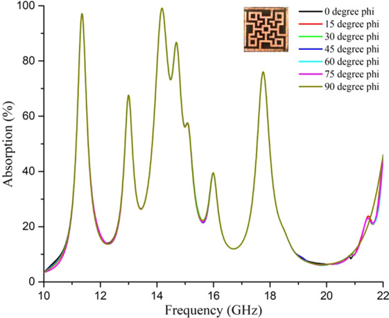
Absorption at normal incidence from simulation (TEM mode).
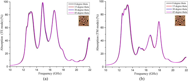
The simulated absorptions for plane-polarized EM waves at different oblique incidences for TE (transverse electric) mode and TM (transverse magnetic) mode of applied incident waves are plotted in Fig. 4(a,b) respectively.
Figure 4.
Absorption from simulation for oblique incidence at (a) TE mode and (b) TM mode operation.
It is observed in Fig. 4(a) that, a considerable bandwidth of absorption (≈1.75 GHz) is ensured from the oblique incidence of applied EM waves on the proposed absorber in TE mode. Broadband absorption is achieved from 12.7 GHz to 13.46 GHz, 14.72 GHz to 15.19 GHz and 16.45 GHz to 16.97 GHz considering −10dB value of S11 and S21 parameters. Whereas in TM mode of applied EM wave at oblique incidence (Fig. 4(b)), the bandwidth of absorption reduces significantly to ≈1.24 GHz. It is important to mention that, in both TE and TM mode for oblique incidence, the proposed absorber can absorb only at Ku band, but bandwidth is increased compared to normal incidence.
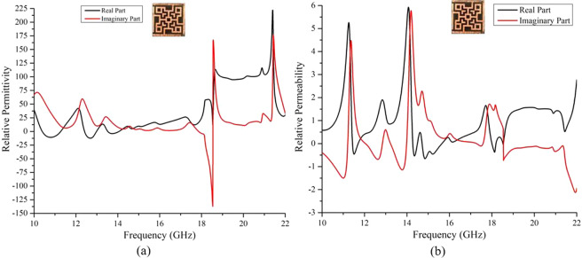
At the resonance frequencies, the value of either relative permittivity or relative permeability was found negative as shown in Fig. 5, which ensures the negative value of the refractive index as per Eq. 4 & 7. Hence the absorption of applied EM waves at normal and oblique incidences is justified from the negative value of the refractive index.
Figure 5.
(a) Relative permittivity and (b) relative permeability of the absorber (from simulation) at operating frequencies.
The impedance of the unit cell in the whole operating frequencies is shown in Fig. 6. Impedance was determined by Eq. 320.
Figure 6.
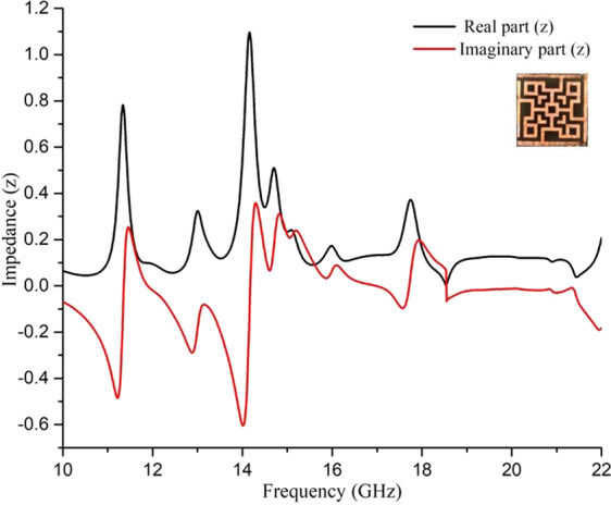
Impedance of the unit cell at operating frequencies.
From Fig. 6 it is clear that the impedance of the unit cell at the resonance frequencies aligns with the impedance of air, as a result, the reflection coefficient is less in these resonance frequencies as shown in Fig. 7. In association with transmission blocked by the metal ground, four absorption peaks were found at 11.31 GHz, 14.11 GHz, 14.23 GHz, and 17.79 GHz respectively.
Figure 7.
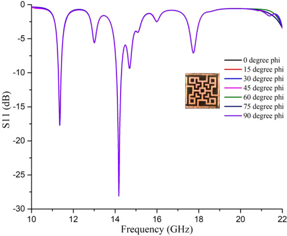
Reflection coefficient for normal incidences at operating frequencies.
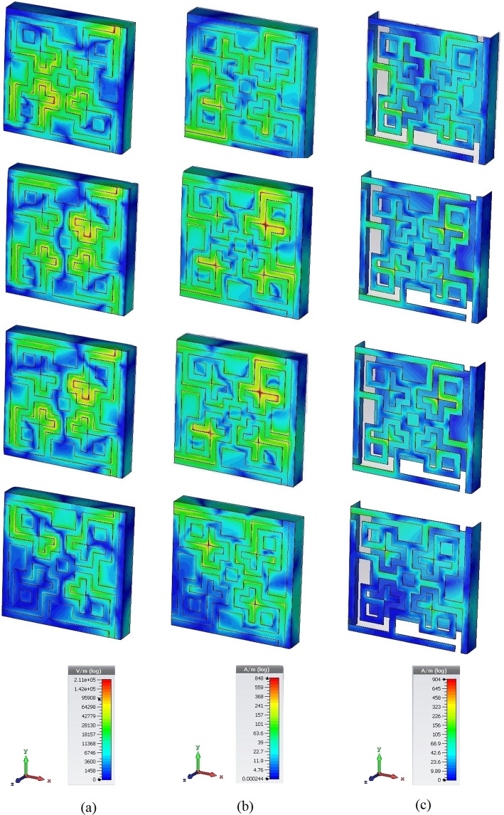
The behavior of the patch along with the ground at the resonance frequencies can be better understood by the following Fig. 8. The perfect electric field was applied along the x-axis, perfect magnetic field along the y-axis and the EM wave propagated along the z-axis. Hence Ez = 0 and Hz = 0 It is essential to mention that, the distributed fields and surface current are lying on the x-y plane. Hence the electric field has components Ex and Ey. Similarly surface current and magnetic fields have Hx, Hy, and Jx, Jy components respectively in Fig. 8. The electric field, magnetic field and current distributions at resonance frequencies show the respective dense amounts at some specific portions of the patch. The redder color shows the dense field and current density. Green color shows medium dense areas and blue means less dense. At the lowest resonance frequency (11.31 GHz), the lower-left corner of the patch seems to be agitated much than the upper right corner. And the right bottom and the upper left corners are comparatively less agitated. But in medium resonance frequencies (14.11 GHz and 14.23 GHz), all four corners are agitated. Hence highest absorption was found in these frequencies. Again, in the highest resonance frequency (17.79 GHz), all the corners except the lower-left corner are agitated. These happen because of the current flow throughout the patch transmission lines, which were changing directions with respect to frequencies. The distributions shown in Fig. 6 are polarization insensitive due to the symmetric geometry of the unit cell. In other words, the magnetic dipoles are aligned with the incident polarized magnetic field and hence the energy due to the incident magnetic field is trapped, which led to less reflection of EM waves and intense absorption inside the lossy dielectric material.
Figure 8.
Instantaneous distribution of (a) electric field, (b) magnetic field, and (c) surface current at 11.31, 14.11, 14.23 and 17.79 GHz, respectively.
Discussion
MM absorbers are designed to use for a perfect absorption of EM waves and other applications like sensing or imaging21–23. High-loss dielectric materials are needed for a wide bandwidth of absorption and curtailed thickness of the substrate. Whereas, for sensing or imaging applications, low-loss dielectric materials are appropriate24. For wideband absorption in the X and Ku band region, the proposed unit cell was designed. The simulated results were justified by taking measured data from VNA and were compared as shown in Fig. 9.
Figure 9.
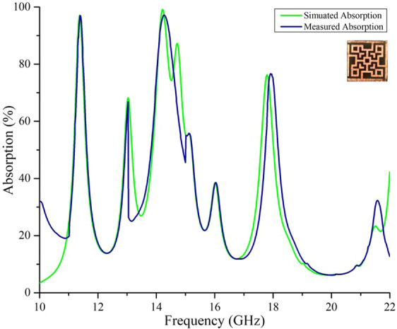
Simulated and measured absorption.
The simulated and measured data are quite similar except few deviations from resonance frequencies at the higher range. This is because the measured data were taken from two different waveguide ports (one port for 10–15 GHz and another port for 15–22 GHz). Absorption was calculated by Eq. 1, which needed S11 and S21 parameters. Hence for comparing the absorption by experimental data with simulated absorption, the total number of sample frequency points (from 10 GHz to 22 GHz) along the x-axis were taken equally. The changing of ports during measurement has caused some changes in expected values. Moreover, the high dielectric loss in the FR4 substrate at higher frequencies may be another reason and hence we see discrepancies in Fig. 9. The bandwidth of absorption is observed wide in Fig. 9. It is assumable that the proposed absorber can only absorb some fractions of the entire incident EM wave because the values of S11 and S21 parameters at the frequencies other than resonance have values more than −10 dB and hence there were absorptions less than 70%. As the substrate is a lossy material (FR4), it only has shown the necessary magnetic dipole momenta at the resonance frequencies.
The performance of the proposed absorber unit cell was compared with recent relevant works (by FR4 substrate) and found it more efficient in terms of response to wide-angle polarized TEM wave, maximum absorption and wide bandwidth of absorption along with the maximum number of resonance frequencies in X and Ku band as shown in Table 2.
Table 2.
Comparison of proposed work with recent relevant works.
| Reference | Year | Substrate Material | Copper patch only | Frequency Bands | Cell Structure Symmetry | Resonance Frequencies (GHz) | Unit Cell Size (mm×mm) | Polarization Insensitivity | Max Absorption (%) | The bandwidth of Absorbed Frequency (GHz) |
|---|---|---|---|---|---|---|---|---|---|---|
| [25] | 2017 | FR4 | Yes | Ku | Yes | 14.75, 15.1, 16.25 | 24 × 24 | Up to 60° | 95% | 1.1 |
| [26] | 2017 | FR4 | Yes | X | Yes | 8.08, 11.41 | 10 × 10 | Up to 30° | 98.97% | 0.4 |
| [13] | 2017 | FR4 | Yes | X | Yes | 10.1–10.6 | 17.6 × 17.6 | Up to 70° | 96.5% | 0.35 |
| [27] | 2017 | FR4 | Yes | X | Yes | 9.26 | 10 × 10 | Up to 70° | 95.28% | 0.3 |
| [28] | 2018 | FR4 | No | X and Ku | Yes | 9, 11, 13 | 15 × 15 | Up to 65° | 99% | Unknown |
| [29] | 2019 | FR4 | Yes | C, X, and Ku | Yes | 5.57, 7.96, 13.44 | 10 × 10 | Up to 75° | 99.28% | 0.34 |
| [16] | 2019 | FR4 | Yes | X and Ku | Yes | 8.6, 10.2, 11.95 | 10 × 10 | Up to 60° | 99.98% | 1.05 |
| Our Proposed Work | 2019 | FR4 | Yes | X and Ku | Yes |
11.21–11.49 13.92–14.85 17.66–17.87 |
10 × 10 | Up to 90° | 99.15% | 1.42 |
Methods
Measurement
The unit cell was practically fabricated (as shown in Fig. 2) to test its absorbance from S parameters by Agilent PNA Network Analyzer N5227A with two different wave-guide ports (one is for 10–15 GHz and another one is for 15–22 GHz) connected simultaneously to the 2 ports of the VNA. In the simulation, the total number of points was 1021 (up to 15 GHz, 430 points and from 15.0119 GHz to 22 GHz, 591 points). To match experimental data with simulation, the number of points for the two waveguide ports were also set to 430 and 591 respectively on VNA and then combined to extract absorptions. As we have used two different waveguide ports, we had to calibrate the VNA setup for 10 to 15 GHz first for the first waveguide port for measurement and then calibrate again from 15 GHz to 22 GHz to measure using the second port. Calibration (e-cal) was done with Agilent N4694-60001 Electronic Calibration Module. S parameters (S11 and S21) were taken in real and imaginary parts separately and copied to an Excel file. Absorption was found from Matlab using data from the Excel file with the necessary codes. The measured values are quite similar to simulated values, which proves it a strong candidate for the absorption purpose in X and Ku band applications with features like the wide-incidence, angle, and polarization insensitivity and broad-bandwidth of frequencies absorptions.
Author contributions
Saif Hannan designed the proposed absorber, analyzed, evaluated the fabricated absorber and wrote the manuscript. Mohammad Tariqul Islam supervised the whole study and provided intellectual suggestions. Ali. F. Almutairi revised the article critically and advised intellectual recommendations. Mohammad Rashed Iqbal Faruque helped in revising the article as per reviewers’ comments.
Competing interests
The authors declare no competing interests.
Footnotes
Publisher’s note Springer Nature remains neutral with regard to jurisdictional claims in published maps and institutional affiliations.
Contributor Information
Saif Hannan, Email: p98220@siswa.ukm.edu.my.
Mohammad Tariqul Islam, Email: tariqul@ukm.edu.my.
Ali F. Almutairi, Email: ali.almut@ku.edu.kw
References
- 1.Valentine J, et al. Three-dimensional optical metamaterial with a negative refractive index. nature. 2008;455:376. doi: 10.1038/nature07247. [DOI] [PubMed] [Google Scholar]
- 2.Faruque MRI, Islam MT, Misran N. Electromagnetic (EM) absorption reduction in a muscle cube with metamaterial attachment. Medical engineering & physics. 2011;33:646–652. doi: 10.1016/j.medengphy.2010.12.004. [DOI] [PubMed] [Google Scholar]
- 3.Cheng Y, He B, Zhao J, Gong R. Ultra-thin low-frequency broadband microwave absorber based on magnetic medium and metamaterial. Journal of Electronic Materials. 2017;46:1293–1299. doi: 10.1007/s11664-016-5115-z. [DOI] [Google Scholar]
- 4.Hannan S, Islam MT, Hoque A, Singh MJ, Almutairi AF. Design of a Novel Double Negative Metamaterial Absorber Atom for Ku and K Band Applications. Electronics. 2019;8:853. doi: 10.3390/electronics8080853. [DOI] [Google Scholar]
- 5.Cheng Y, Cheng Z, Mao X, Gong R. Ultra-thin multi-band polarization-insensitive microwave metamaterial absorber based on multiple-order responses using a single resonator structure. Materials. 2017;10:1241. doi: 10.3390/ma10111241. [DOI] [PMC free article] [PubMed] [Google Scholar]
- 6.Ayop O, Rahim MKA, Murad NA, Samsuri NA. Dual-resonant polarization-independent and wide-angle metamaterial absorber in X-band frequency. Applied Physics A. 2016;122:374. doi: 10.1007/s00339-016-9902-4. [DOI] [Google Scholar]
- 7.Tung BS, et al. Polarization-independent, wide-incident-angle and dual-band perfect absorption, based on near-field coupling in a symmetric metamaterial. Scientific reports. 2017;7:11507. doi: 10.1038/s41598-017-11824-7. [DOI] [PMC free article] [PubMed] [Google Scholar]
- 8.Cong L-L, Cao X-Y, Song T, Han T. Polarization-independent wide-angle ultrathin double-layered metamaterial absorber for broadband application. Applied Physics A. 2018;124:452. doi: 10.1007/s00339-018-1686-2. [DOI] [Google Scholar]
- 9.Barde, C., Choubey, A. & Sinha, R. A set square design metamaterial absorber for X-band applications. Journal of Electromagnetic Waves and Applications, 1–14 (2019).
- 10.Islam M, Islam M, Samsuzzaman M, Faruque M, Misran N. A negative index metamaterial-inspired UWB antenna with an integration of complementary SRR and CLS unit cells for microwave imaging sensor applications. Sensors. 2015;15:11601–11627. doi: 10.3390/s150511601. [DOI] [PMC free article] [PubMed] [Google Scholar]
- 11.Cheng Y, Nie Y, Wang X, Gong R. Adjustable low frequency and broadband metamaterial absorber based on magnetic rubber plate and cross resonator. Journal of Applied Physics. 2014;115:064902. doi: 10.1063/1.4863540. [DOI] [Google Scholar]
- 12.Hasan M, Faruque M, Islam S, Islam M. A new compact double-negative miniaturized metamaterial for wideband operation. Materials. 2016;9:830. doi: 10.3390/ma9100830. [DOI] [PMC free article] [PubMed] [Google Scholar]
- 13.Nguyen TT, Lim S. Bandwidth-enhanced and Wide-angle-of-incidence Metamaterial Absorber using a Hybrid Unit Cell. Scientific reports. 2017;7:14814. doi: 10.1038/s41598-017-14792-0. [DOI] [PMC free article] [PubMed] [Google Scholar]
- 14.Liu L, Chen J, Zhou Z, Yi Z, Ye X. Tunable absorption enhancement in electric split-ring resonators-shaped graphene arrays. Materials Research Express. 2018;5:045802. doi: 10.1088/2053-1591/aabbd9. [DOI] [Google Scholar]
- 15.Luo H, Cheng YZ. Ultra-thin dual-band polarization-insensitive and wide-angle perfect metamaterial absorber based on a single circular sector resonator structure. Journal of Electronic Materials. 2018;47:323–328. doi: 10.1007/s11664-017-5770-8. [DOI] [Google Scholar]
- 16.Jafari FS, Naderi M, Hatami A, Zarrabi FB. Microwave Jerusalem cross absorber by metamaterial split ring resonator load to obtain polarization independence with triple band application. AEU-International Journal of Electronics and Communications. 2019;101:138–144. doi: 10.1016/j.aeue.2019.02.002. [DOI] [Google Scholar]
- 17.Grześkiewicz B, Sierakowski A, Marczewski J, Pałka N, Wolarz E. SU-8 based planar metamaterials with fourfold symmetry as selective terahertz absorbers. Opto-Electronics Review. 2018;26:329–337. doi: 10.1016/j.opelre.2018.10.006. [DOI] [Google Scholar]
- 18.Cheng Y, Zou Y, Luo H, Chen F, Mao X. Compact Ultra-Thin Seven-Band Microwave Metamaterial Absorber Based on a Single Resonator Structure. Journal of Electronic Materials. 2019;48:3939–3946. doi: 10.1007/s11664-019-07156-z. [DOI] [Google Scholar]
- 19.Misran N, Yusop SH, Islam MT, Ismail MY. Analysis of Parameterization Substrate Thickness and Permittivity for Concentric Split Ring Square Reflectarray Element. Jurnal Kejuruteraan (Journal of Engineering) 2012;23:11–16. [Google Scholar]
- 20.Chen X, Grzegorczyk TM, Wu B-I, Pacheco J, Jr., Kong JA. Robust method to retrieve the constitutive effective parameters of metamaterials. Physical review E. 2004;70:016608. doi: 10.1103/PhysRevE.70.016608. [DOI] [PubMed] [Google Scholar]
- 21.Yoo Y, et al. Triple-band perfect metamaterial absorption, based on single cut-wire bar. Applied Physics Letters. 2015;106:071105. doi: 10.1063/1.4913243. [DOI] [Google Scholar]
- 22.Wang B-X, Zhai X, Wang G-Z, Huang W-Q, Wang L-L. A novel dual-band terahertz metamaterial absorber for a sensor application. Journal of Applied Physics. 2015;117:014504. doi: 10.1063/1.4905261. [DOI] [Google Scholar]
- 23.Kuznetsov SA, Paulish AG, Gelfand AV, Lazorskiy PA, Fedorinin VN. Matrix structure of metamaterial absorbers for multispectral terahertz imaging. Progress In Electromagnetics Research. 2012;122:93–103. doi: 10.2528/PIER11101401. [DOI] [Google Scholar]
- 24.Assimonis SD, Fusco V. Polarization Insensitive, Wide-Angle, Ultra-wideband, Flexible, Resistively Loaded, Electromagnetic Metamaterial Absorber using Conventional Inkjet-Printing Technology. Scientific reports. 2019;9:1–15. doi: 10.1038/s41598-019-48761-6. [DOI] [PMC free article] [PubMed] [Google Scholar]
- 25.Naser-Moghadasi M, Nia AZ, Toolabi M, Heydari S. Microwave metamaterial Absorber based on Jerusalem Cross with meandered load for bandwidth enhancement. Optik. 2017;140:515–522. doi: 10.1016/j.ijleo.2017.04.007. [DOI] [Google Scholar]
- 26.Hossain M, Faruque M, Islam M, Mat K. A new compact octagonal shape perfect metamaterial absorber for microwave applications. Applied Sciences. 2017;7:1263. doi: 10.3390/app7121263. [DOI] [Google Scholar]
- 27.Nguyen TT, Lim S. Wide incidence angle-insensitive metamaterial absorber for both TE and TM polarization using eight-circular-sector. Scientific reports. 2017;7:3204. doi: 10.1038/s41598-017-03591-2. [DOI] [PMC free article] [PubMed] [Google Scholar]
- 28.Nguyen TT, Lim S. Design of metamaterial absorber using eight-resistive-arm cell for simultaneous broadband and wide-incidence-angle absorption. Scientific reports. 2018;8:6633. doi: 10.1038/s41598-018-25074-8. [DOI] [PMC free article] [PubMed] [Google Scholar]
- 29.Dhillon AS, Mittal D, Bargota R. Triple band ultrathin polarization insensitive metamaterial absorber for defense, explosive detection and airborne radar applications. Microwave and Optical Technology Letters. 2019;61:89–95. doi: 10.1002/mop.31547. [DOI] [Google Scholar]


