

Abstract

Investigating group-IV-based photonic components is a very active area of research with extensive interest in developing complementary metal-oxide-semiconductor (CMOS) compatible light sources. However, due to the indirect band gap of these materials, effective light-emitting diodes and lasers based on pure Ge or Si cannot be realized. In this context, there is considerable interest in developing group-IV based Raman lasers. Nevertheless, the low quantum yield of stimulated Raman scattering in Si and Ge requires large device footprints and high lasing thresholds. Consequently, the fabrication of integrated, energy-efficient Raman lasers is challenging. Here, we report the systematic investigation of stimulated Raman scattering (SRS) in Ge nanowires (NWs) and axial Al-Ge-Al NW heterostructures with Ge segments that come into contact with self-aligned Al leads with abrupt metal–semiconductor interfaces. Depending on their geometry, these quasi-one-dimensional (1D) heterostructures can reassemble into Ge nanowires, Ge nanodots, or Ge nanodiscs, which are monolithically integrated within monocrystalline Al (c-Al) mirrors that promote both optical confinement and effective heat dissipation. Optical mode resonances in these nanocavities support in SRS thresholds as low as 60 kW/cm2. Most notably, our findings provide a platform for elucidating the high potential of future monolithically integrated, nanoscale low-power group-IV-based Raman lasers.
Introduction
The continuing miniaturization of Si-based integrated circuits has led to high-performance compact devices with reduced power consumption at lower cost.1−3 Associated with this rapid downscaling, metallic interconnects have become a severe bottleneck due to their high space demand, signal delays, and electromagnetic interference.4,5 Thus, there is an increasing demand for high-speed data transmission in the optical domain.6 While effective on-chip detection and transmission have already been demonstrated,7 conventional light-emitting diodes and lasers based on pure Si or Ge cannot be realized, due to their indirect band gap. In this context, there is considerable interest in developing group-IV-based Raman lasers. Nevertheless, the low quantum yield of stimulated Raman scattering (SRS) in Si and Ge requires large device footprints and high lasing thresholds.8,9 These centimeter-scale lasers are incompatible with the goal of fabricating on-chip energy-efficient monolithically integrable lasers.10,11 Meanwhile, semiconducting nanowires (NWs) may possess great future potential due to their quasi-one-dimensional (1D) cylindrical geometry and easy device integration.12,13 In terms of optoelectronic devices, it was already demonstrated that NWs can function as both active optical device elements14 and transmission lines.15 Lasers fabricated from direct band gap semiconductor NWs have been achieved using GaN,16 ZnO,13 and CdS.17 However, there are only a few works on NW-based Raman lasers, including the pioneering work on cavity-enhanced SRS in GaP NWs18 and cavity-mode enhanced SRS in Si NWs.19,20 To our knowledge, there are no further reports on this important nonlinear optical effect in semiconductor NWs.
Methods
Device Fabrication
Vapor–liquid–solid21 (VLS)-grown Ge NWs with a length of several micrometers and diameters ranging from 40 nm to 140 nm were dispersed onto a Si substrate with 100 nm of thermally grown SiO2 atop. To synthesize the Al-Ge-Al NW heterostructures, Ge NWs with diameters of 100 nm were brought into contact with Al pads fabricated by electron beam lithography, 150 nm Al sputter deposition, preceded by a 5 s HI dip (14%) to remove any Ge oxide, and lift-off techniques. The Al-Ge exchange reaction is induced by rapid thermal annealing (UniTemp UTP 1100) at a temperature of T = 624 K in forming a gas atmosphere and results in quasi-1D NW heterostructures. To achieve small Ge nanostructure devices, such as nanodots and nanodiscs, consecutive thermal annealing steps were applied, accompanied by SEM imaging.22,23
Raman Measurements
A confocal μ-Raman setup (Alpha300, WITec) was employed in backscattering geometry with a grating monochromator and a CCD camera (DV401- BV, Andor). A frequency-doubled Nd:YAG laser emitting linearly polarized light at λ = 532 nm was used as an excitation source. The laser light passes a beam splitter with an integrated polarizer and is focused onto the sample surface through an achromatic Nikon EPI EPlan 100 x objective (NA = 0.9, WD = 0.23 mm), enabling a diffraction-limited spot size of ∼720 nm. The scattered light was confocally collected through the objective and filtered to remove the excitation wavelength and then coupled into a fiber that guides the light to the spectrometer.
FDTD Simulations
Numerical three-dimensional (3D) finite
difference time domain (FDTD) calculations were performed (based on
the commercially available software Lumerical FDTD) at λ = 532
nm incident wavelength to estimate the strength of the Raman effect
from the Ge TO mode. The electrical energy inside the Ge segment was
calculated by integrating the simulated integrated field intensity
over the entire Ge volume  with n2 = εr*μr and μr = 1, where εr is the relative permittivity and μr is the relative
permeability. The data are typically normalized to the peak value,
and hence
with n2 = εr*μr and μr = 1, where εr is the relative permittivity and μr is the relative
permeability. The data are typically normalized to the peak value,
and hence  cancels out within the fraction to provide
a relative local field enhancement factor. When estimating the relative
strength of Raman scattering between different Ge nanostructures,
the calculated data per Ge volume was corrected by the measured signal
decrease due to the temperature increase in the NW segment as explained
in the Supporting Information.
cancels out within the fraction to provide
a relative local field enhancement factor. When estimating the relative
strength of Raman scattering between different Ge nanostructures,
the calculated data per Ge volume was corrected by the measured signal
decrease due to the temperature increase in the NW segment as explained
in the Supporting Information.
Results and Discussion
In this paper, we present a systematic experimental investigation of Raman scattering in Ge nanostructures. The VLS- grown Ge NWs with a length of several micrometers and diameters ranging from 40 to 140 nm were dispersed onto a Si substrate with 100 nm of thermally grown SiO2 atop. Raman spectroscopy was performed using a confocal μ-Raman setup with CW laser excitation at λpump = 532 nm. A schematic illustration of the μ-Raman experiments on Ge NWs in backscattering geometry is shown in Figure 1a. The Stokes Raman spectra of an NW with a diameter of 100 nm for pump laser intensities between 8 and 200 kW/cm2 are shown in Figure 1b. The Raman spectra reveal two distinct peaks assigned to the Stokes transverse optical (TO) modes of Ge–Ge vibrations (Ge TO) at about 301 cm–1 and the Si–Si vibrations (Si TO) of the underlying Si substrate at 520 cm–1.24−26 With increasing pump laser intensity, both the TO modes increase in intensity but only the Ge-related Raman peak undergoes a slight red shift. The inset shows the red shift of the TO phonon mode of a 2 μm long (black) Ge NW and a 100 nm long (red) Ge NW for increasing pump intensities up to 190 kW/cm2. This red shift is associated with laser-induced heating. The more pronounced red shift of the Ge TO phonon mode is consistent with the lower thermal mass of the shorter Ge NW.24,27
Figure 1.

(a) Schematic illustration of μ-Raman experiments on Ge NWs in backscattering geometry and confocal detection. (b) Exemplary Stokes Raman spectra of a Ge NW with a diameter of 100 nm and a length of 2 μm for laser excitation (λpump = 532 nm) with intensities between 8 and 190 kW/cm2. The Raman spectrum shows the TO modes at 301 and 520 cm–1 assigned to Ge-Ge and Si-Si vibrations of the Ge NW and the underlying Si substrate, respectively. The inset shows the red shift of the Ge TO phonon mode for a 2 μm long (black) and a 100 nm long (red) Ge NW for pump intensities up to 190 kW/cm2.
According to the work of Agarwal et al.19,20 cavity-mode enhanced SRS in Si NWs was demonstrated to arise from higher electric field intensity and lower mode volume of the electromagnetic modes inside the quasi-1D nanostructures. To investigate the dependence of the Stokes intensity of the Ge TO peak on the Ge NW diameter, numerical calculations were performed to calculate the electric energy confined to the Ge NW via the finite difference time domain (FDTD) method.19,28 The calculations shown in Figure 2a clearly reveal that for λpump = 532 nm, the highest electric field intensity is observed for Ge NWs with a diameter of about 100 nm. The calculations were then compared with the integrated Ge TO Stokes intensity of Ge NWs with diameters between 40 and 140 nm. As heating not only induces red shifts but also decreases the Stokes intensity,29 the recorded spectra were corrected for these temperature effects (see Figure S1). As shown in Figure 2b, Ge NWs with a diameter of 100 nm show the highest Stokes intensity. In all of these cases, the Stokes intensity of the Ge TO peak increases linearly with the pump intensity, indicating spontaneous Raman scattering.19
Figure 2.

(a) FDTD calculation of the spatial distribution of the electric field intensity inside Ge NWs of various diameters as a function of excitation wavelength. (b) Normalized integrated Stokes intensity of the Ge TO peak of 2 μm long Ge NWs with different diameters at various pump intensities. The μ-Raman measurements were obtained using a λ = 532 nm pump laser and corrected with respect to thermal effects.
To cope with the problem of laser-induced heating and to further achieve and explore SRS, Ge NWs were monolithically integrated in metal–semiconductor–metal (M-S-M) NW heterostructures (Figure 3a). Therefore, the Ge NWs on the oxidized Si substrate were brought into contact with 150 nm thick Al pads using electron beam lithography, Al sputter deposition preceded by 5 s HI dip (14%), and lift-off techniques. To adjust the Ge NW segment length, a thermally induced exchange reaction was applied using rapid thermal annealing.22,23 This results in axial Al-Ge-Al NW heterostructures with ultrascaled Ge segments that came into contact with both sides by self-aligned monocrystalline Al leads with abrupt M–S interfaces (see Figures S2 and S3). The schematics and SEM images in Figure 3b show such Al-Ge-Al NW heterostructures with typical Ge geometries further denoted as the Ge segment (L > d), the Ge nanodot (L ≈ d), and the Ge nanodisc (L < d).
Figure 3.

(a) Schematic illustration of μ-Raman experiments on Al-Ge-Al NW heterostructures in backscattering geometry. (b) Schematic illustration and SEM images of a Ge segment (L > d), a Ge nanodot (L ≈ d), and a Ge nanodisc (L < d) monolithically integrated in an Al-Ge-Al NW heterostructure.
The c-Al leads contacting the Ge segments are expected to effectively dissipate the energy introduced by laser excitation. Figure 4a shows the Raman shift and the corresponding calculated temperature increases at various laser pump intensities for a 100 nm long Ge NW and a Ge segment of the same length embedded in the Al-Ge-Al NW heterostructure (dashed and solid red lines, respectively). As expected, the bare Ge NW heats up significantly more than the Al-Ge-Al NW heterostructure device. This is attributed to efficient heat transfer by the c-Al contact leads and dissipation by the large Al heat sinks. This is further supported by the investigation of various heterostructure devices between L = 500 and 20 nm, which revealed significantly lower laser-induced heating effects for even smaller Ge segments.
Figure 4.

(a) Comparison of the laser heating effect on the Raman shift of Ge NWs and Al-Ge-Al NW heterostructures all with a diameter of 100 nm. (b) Polar representation of the normalized angle-dependent integrated Stokes intensities of the Ge TO peak of a Ge NW (black), a Ge nanodot (red), and a Ge nanodisc (blue). All μ-Raman measurements were obtained using a λ = 532 nm pump laser.
Figure 4b shows a comparison of the normalized angle-dependent integrated Ge TO Stokes intensities of a Ge segment, a Ge nanodot, and a Ge nanodisc all integrated within Al-Ge-Al NW heterostructures. Here, the electric field polarization is being rotated from being parallel (transverse magnetic, TM) to being perpendicular (transverse electric, TE) to the NW axis. Elongated Ge NWs (black) exhibit the highest integrated Stokes intensity of the Ge TO peak when the incident polarization is parallel to the NW axis. The anisotropic Raman scattering can be explained by considering the effect of the dielectric permittivity mismatch of the NW geometry.30,31 In contrast, the Ge nanodisc (blue) shows much less anisotropy and the Stokes intensity of the Ge TO peak was found to be larger for the pump laser polarized perpendicular to the NW axis, i.e., parallel to the elongated Ge nanodisc, which can again be associated with the dielectric permittivity mismatch of the geometry. However, according to the particular geometry of the nanodisc devices, this effect was found to be quite weak. Finally, the Ge nanodot (red) shows no preferential polarization axis. Based on these investigations, the Raman response of the respective devices was maximized for the following investigations choosing the proper laser polarization.
Importantly, the effective heat dissipation in Al-Ge-Al NW heterostructures compared to bare Ge NW devices allows the investigation of Raman scattering for higher excitation intensities without thermally damaging these devices. Determining the integrated Stokes intensity as a function of the excitation power requires subtraction of the enhanced background observed for the Al-Ge-Al heterostructures (see Figure S4). The integrated Stokes intensity of the Ge TO peak was further normalized by Ge volume for varying Ge segment length L, as a function of the pump intensity is shown in Figure 5a. Devices with L ≥ 300 nm show a linear increase of the integrated Stokes intensity of the Ge TO peak for all investigated pump intensities, indicating that merely spontaneous Raman scattering occurs. In contrast, the integrated Stokes intensity of the Ge TO peak of devices with L = 20, 50, and 100 nm became nonlinear for sufficiently high pump intensities, suggesting the onset of SRS. Considering the smallest 20 nm long Ge nanodisc heterostructure device at a pump intensity of 60 kW/cm2, the integrated Stokes intensity of the Ge TO peak was twice the value calculated from linear extrapolation at the lowest pump intensities, corresponding to a 100% enhancement in Stokes scattering. A comparison of the integrated Ge TO signal to the substrate related Si TO and SiO2 signals is shown in Figure S5.
Figure 5.

(a) Temperature-corrected integrated Stokes intensity of the Ge TO peak for Al-Ge-Al NW heterostructures as a function of the pump intensity normalized with respect to the volume of the Ge segment. Ge segment lengths vary between 20 nm and 1 μm. The solid lines are guidance for the eye. (b) Evaluation of the normalized integrated Stokes intensity of the Ge TO peak at 256 kW/cm2 pump intensity as a function of the Ge segment length L. The inset schematically shows the transition from heterostructure devices with Ge segments to Ge nanodiscs. All μ-Raman measurements were obtained using a λ = 532 nm pump laser. (c) Calculated electric field energy for bare Ge NWs (blue) and Al-Ge-Al NW heterostructures (red) normalized by both Ge volume and the effect of relative heating. The temperature corrections for (c) are shown in the supporting information (cf. Figure S6). The inset shows cross-sections of the field intensity distributions (|Ep (r)|2/|E0|2) in the Ge segments for L = 20, 50, and 300 nm.
Figure 5b shows the evaluation of the normalized integrated Stokes intensity of the Ge TO peak at a pump intensity of 256 kW/cm2 as a function of the Ge segment length. The rapid increase in electric energy for Ge segment lengths <100 nm indicates a nanocavity effect within the Al-Ge-Al NW heterostructure device geometry.
The spontaneous
Raman signal strength, SR, depends on
the electric field energy, 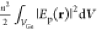 , within the Ge volume, VGe, where Ep (r) is the incident
electric field. It will also be affected by temperature,
which can be taken into account by a correction function determined
from the experiments, f(L). We thus
can write the normalized Raman signal per unit volume as
, within the Ge volume, VGe, where Ep (r) is the incident
electric field. It will also be affected by temperature,
which can be taken into account by a correction function determined
from the experiments, f(L). We thus
can write the normalized Raman signal per unit volume as 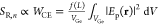 , where WCE has
units of electric energy density. Calculations of WCE are depicted for the bare Ge NW as well as the Al-Ge-Al
heterostructure in Figure 5c. The correction data f(L) and the noncorrected calculations are also shown for comparison
in Figure S6. Most notably, the electric
energy density increases for L < 100 nm in the
Al-Ge-Al heterostructure (red dashed line), which indicates good optical
confinement. This is in stark contrast to the Ge-only case, which
shows a strong decrease for L < 100 nm (blue dashed
line), indicating the loss of optical confinement. In fact, very little
of the electric field penetrates the NW for segments of length, L < 100 nm, as shown in the inset of Figure 5c. For the Al-Ge-Al heterostructure
(inset Figure 5c, upper
row), a hybrid plasmonic mode exists allowing for nonvanishing fields
within the Ge even for the very shortest Ge segments. Note that this
is in line with the results from the study of Fan et al.,32 where a Ge NW resonance was cascaded with a
metallic slit resonance formed between two narrow metal electrodes
to support standing wave resonances of gap surface plasmon polaritons.33,34 These experimental observations and field calculations show that
the metallic contacts are key to observing SRS within the narrow Ge-segment
regime. The Al contacts to the Ge provide two functions: (1) optical
confinement via a hybrid plasmonic mode to ensure a sufficiently large
electric energy density to trigger SRS and (2) the mitigation of Ge
heating under intense laser excitation.
, where WCE has
units of electric energy density. Calculations of WCE are depicted for the bare Ge NW as well as the Al-Ge-Al
heterostructure in Figure 5c. The correction data f(L) and the noncorrected calculations are also shown for comparison
in Figure S6. Most notably, the electric
energy density increases for L < 100 nm in the
Al-Ge-Al heterostructure (red dashed line), which indicates good optical
confinement. This is in stark contrast to the Ge-only case, which
shows a strong decrease for L < 100 nm (blue dashed
line), indicating the loss of optical confinement. In fact, very little
of the electric field penetrates the NW for segments of length, L < 100 nm, as shown in the inset of Figure 5c. For the Al-Ge-Al heterostructure
(inset Figure 5c, upper
row), a hybrid plasmonic mode exists allowing for nonvanishing fields
within the Ge even for the very shortest Ge segments. Note that this
is in line with the results from the study of Fan et al.,32 where a Ge NW resonance was cascaded with a
metallic slit resonance formed between two narrow metal electrodes
to support standing wave resonances of gap surface plasmon polaritons.33,34 These experimental observations and field calculations show that
the metallic contacts are key to observing SRS within the narrow Ge-segment
regime. The Al contacts to the Ge provide two functions: (1) optical
confinement via a hybrid plasmonic mode to ensure a sufficiently large
electric energy density to trigger SRS and (2) the mitigation of Ge
heating under intense laser excitation.
Conclusions
We have systematically investigated Raman scattering in Ge NWs as well as axial Al-Ge-Al NW heterostructures with abrupt metal–semiconductor interfaces. We demonstrated that these quasi-1D heterostructures can be reassembled into Ge segments that are monolithically integrated between c-Al mirrors that also serve as effective heat sinks. Plasmonic mode resonances within these nanocavities result in SRS with thresholds as low as 60 kW/cm2. This is a significant step toward the development of a homogeneous group-IV nanolaser with a low lasing threshold, which could lead to the development of the first monolithically integrable Ge-based Raman nanolaser in the infrared as well as telecom wavelength range.
Acknowledgments
The authors gratefully acknowledge financial support from the Austrian Science Fund (FWF): project no. P29729-N27. The authors further thank the Center for Micro- and Nanostructures for providing cleanroom facilities. We acknowledge support from the Laboratoire d’excellence LANEF in Grenoble (ANR-10-LABX-51-01). Financial support from the ANR-COSMOS (ANR-12-JS10-0002) project is acknowledged. We benefitted from the access to the Nano characterization platform (PFNC) in CEA Minatec Grenoble in collaboration with the LEMMA/IRIG group. We acknowledge support from Campus France in the framework of PHC AMADEUS 2016 for project no. 35592PB.
Supporting Information Available
The Supporting Information is available free of charge at https://pubs.acs.org/doi/10.1021/acs.jpcc.0c02602.
Laser-induced heating effects of Ge NWs, transmission electron microscopy (TEM) and energy-dispersive X-ray (EDX) images of Al-Ge-Al NW heterostructures, details regarding the calculation of electric field energy for bare Ge NWs and Al-Ge-Al NW heterostructures with respect to the effect of heating (PDF)
Author Contributions
M.S. and M.G.B. performed the device fabrication. M.S. conducted the Raman measurements. A.L. conceived the project, contributed essentially to the experimental design. N.A.G. conducted the electric field energy calculations and the FDTD field intensity simulations for bare Ge NWs and Al-Ge-Al NW heterostructures. N.A.G. and R.F.O. assisted with the explanation of the underlying physical mechanisms. H.K. performed the numerical calculation of the spatial distribution of the electric field intensity via the FDTD method. M.I.H., E.R., and M.A.L. carried out the TEM and EDX measurements and analysis. All authors analyzed the results and helped shape the research and manuscript.
The authors declare no competing financial interest.
Supplementary Material
References
- Chau R.; Doyle B.; Datta S.; Kavalieros J.; Zhang K. Integrated Nanoelectronics for the Future. Nat. Mater. 2007, 6, 810–812. 10.1038/nmat2014. [DOI] [PubMed] [Google Scholar]
- Moore G. E. Cramming More Components onto Integrated Circuits. IEEE Solid-State Circuits Soc. Newsl. 2006, 11, 33–35. 10.1109/N-SSC.2006.4785860. [DOI] [Google Scholar]
- Thompson S. E.; Parthasarathy S. Moore’s Law: The Future of Si Microelectronics. Mater. Today 2006, 9, 20–25. 10.1016/S1369-7021(06)71539-5. [DOI] [Google Scholar]
- Chaudhry A. Interconnects for Nanoscale MOSFET Technology: A Review. J. Semicond. 2013, 34, 066001 10.1088/1674-4926/34/6/066001. [DOI] [Google Scholar]
- Kaushik B. K.; Goel S.; Rauthan G. Future VLSI Interconnects: Optical Fiber or Carbon Nanotube – a Review. Microelectron. Int. 2007, 24, 53–63. 10.1108/13565360710745601. [DOI] [Google Scholar]
- Soref R. Silicon Photonics: A Review of Recent Literature. Silicon 2010, 2, 1–6. 10.1007/s12633-010-9034-y. [DOI] [Google Scholar]
- Wang K. C.High-Speed Circuits for Lightwave Communications, Selected topics in electronics and systems; World Scientific, 1999. [Google Scholar]
- Claps R.; Raghunathan V.; Dimitropoulos D.; Jalali B. Influence of Nonlinear Absorption on Raman Amplification in Silicon Waveguides. Opt. Express 2004, 12, 2774. 10.1364/OPEX.12.002774. [DOI] [PubMed] [Google Scholar]
- Jalali B.; Fathpour S. Silicon Photonics. J. Lightwave Technol. 2006, 24, 4600–4615. 10.1109/JLT.2006.885782. [DOI] [Google Scholar]
- Rong H.; Jones R.; Liu A.; Cohen O.; Hak D.; Fang A.; Paniccia M. A Continuous-Wave Raman Silicon Laser. Nature 2005, 433, 725–728. 10.1038/nature03346. [DOI] [PubMed] [Google Scholar]
- Rong H.; Xu S.; Kuo Y.-H.; Sih V.; Cohen O.; Raday O.; Paniccia M. Low-Threshold Continuous-Wave Raman Silicon Laser. Nat. Photonics 2007, 1, 232–237. 10.1038/nphoton.2007.29. [DOI] [Google Scholar]
- Appenzeller J.; Knoch J.; Bjork M. T.; Riel H.; Schmid H.; Riess W. Toward Nanowire Electronics. IEEE Trans. Electron Devices 2008, 55, 2827–2845. 10.1109/TED.2008.2008011. [DOI] [Google Scholar]
- Pauzauskie P. J.; Yang P. Nanowire Photonics. Mater. Today 2006, 9, 36–45. 10.1016/S1369-7021(06)71652-2. [DOI] [Google Scholar]
- Li J.; Wang D.; LaPierre R. R.. Advances in III-V Semiconductor Nanowires and Nanodevices; Bentham Science Publishers, 2011. [Google Scholar]
- Wei H.; Pan D.; Zhang S.; Li Z.; Li Q.; Liu N.; Wang W.; Xu H. Plasmon Waveguiding in Nanowires. Chem. Rev. 2018, 118, 2882–2926. 10.1021/acs.chemrev.7b00441. [DOI] [PubMed] [Google Scholar]
- Gradečak S.; Qian F.; Li Y.; Park H.-G.; Lieber C. M. GaN Nanowire Lasers with Low Lasing Thresholds. Appl. Phys. Lett. 2005, 87, 173111 10.1063/1.2115087. [DOI] [Google Scholar]
- Duan X.; Huang Y.; Agarwal R.; Lieber C. M. Single-Nanowire Electrically Driven Lasers. Nature 2003, 421, 241–245. 10.1038/nature01353. [DOI] [PubMed] [Google Scholar]
- Wu J.; Gupta A. K.; Gutierrez H. R.; Eklund P. C. Cavity-Enhanced Stimulated Raman Scattering from Short GaP Nanowires. Nano Lett. 2009, 9, 3252–3257. 10.1021/nl901515t. [DOI] [PubMed] [Google Scholar]
- Agarwal D.; Ren M.-L.; Berger J. S.; Yoo J.; Pan A.; Agarwal R. Nanocavity-Enhanced Giant Stimulated Raman Scattering in Si Nanowires in the Visible Light Region. Nano Lett. 2019, 19, 1204–1209. 10.1021/acs.nanolett.8b04666. [DOI] [PubMed] [Google Scholar]
- Agarwal D.; Yoo J.; Pan A.; Agarwal R. Cavity Engineering of Photon–Phonon Interactions in Si Nanocavities. Nano Lett. 2019, 19, 7950–7956. 10.1021/acs.nanolett.9b03120. [DOI] [PubMed] [Google Scholar]
- Wagner R. S.; Ellis W. C. Vapor-Liquid-Solid Mechanism of Single Crystal Growth. Appl. Phys. Lett. 1964, 4, 89–90. 10.1063/1.1753975. [DOI] [Google Scholar]
- Kral S.; Zeiner C.; Stöger-Pollach M.; Bertagnolli E.; den Hertog M. I.; Lopez-Haro M.; Robin E.; El Hajraoui K.; Lugstein A. Abrupt Schottky Junctions in Al/Ge Nanowire Heterostructures. Nano Lett. 2015, 15, 4783–4787. 10.1021/acs.nanolett.5b01748. [DOI] [PMC free article] [PubMed] [Google Scholar]
- El Hajraoui K.; Luong M. A.; Robin E.; Brunbauer F.; Zeiner C.; Lugstein A.; Gentile P.; Rouvière J.-L.; Den Hertog M. In Situ Transmission Electron Microscopy Analysis of Aluminum–Germanium Nanowire Solid-State Reaction. Nano Lett. 2019, 19, 2897–2904. 10.1021/acs.nanolett.8b05171. [DOI] [PMC free article] [PubMed] [Google Scholar]
- Parker J. H.; Feldman D. W.; Ashkin M. Raman Scattering by Silicon and Germanium. Phys. Rev. 1967, 155, 712–714. 10.1103/PhysRev.155.712. [DOI] [Google Scholar]
- Richter H.; Wang Z. P.; Ley L. The One Phonon Raman Spectrum in Microcrystalline Silicon. Solid State Commun. 1981, 39, 625–629. 10.1016/0038-1098(81)90337-9. [DOI] [Google Scholar]
- Borowicz P.; Latek M.; Rzodkiewicz W.; Łaszcz A.; Czerwinski A.; Ratajczak J. Deep-Ultraviolet Raman Investigation of Silicon Oxide: Thin Film on Silicon Substrate versus Bulk Material. Adv. Nat. Sci.: Nanosci. Nanotechnol. 2012, 3, 045003 10.1088/2043-6262/4/045003. [DOI] [Google Scholar]
- Lugstein A.; Mijić M.; Burchhart T.; Zeiner C.; Langegger R.; Schneider M.; Schmid U.; Bertagnolli E. In Situ Monitoring of Joule Heating Effects in Germanium Nanowires by μ-Raman Spectroscopy. Nanotechnology 2013, 24, 065701 10.1088/0957-4484/24/6/065701. [DOI] [PubMed] [Google Scholar]
- Taflove A.; Hagness S. C.. Computational Electrodynamics: The Finite-Difference Time-Domain Method; Artech House, 2005. [Google Scholar]
- Saltonstall C. B.; Serrano J.; Norris P. M.; Hopkins P. E.; Beechem T. E. Single Element Raman Thermometry. Rev. Sci. Instrum. 2013, 84, 064903 10.1063/1.4810850. [DOI] [PubMed] [Google Scholar]
- Zardo I.; Conesa-Boj S.; Peiro F.; Morante J. R.; Arbiol J.; Uccelli E.; Abstreiter G.; Fontcuberta i Morral A. Raman Spectroscopy of Wurtzite and Zinc-Blende GaAs Nanowires: Polarization Dependence, Selection Rules, and Strain Effects. Phys. Rev. B 2009, 80, 245324 10.1103/PhysRevB.80.245324. [DOI] [Google Scholar]
- Wang J.; Gudiksen M. S.; Duan X.; Cui Y.; Lieber C. M. Highly Polarized Photoluminescence and Photodetection from Single Indium Phosphide Nanowires. Science 2001, 293, 1455–1457. 10.1126/science.1062340. [DOI] [PubMed] [Google Scholar]
- Fan P.; Huang K. C. Y.; Cao L.; Brongersma M. L. Redesigning Photodetector Electrodes as an Optical Antenna. Nano Lett. 2013, 13, 392–396. 10.1021/nl303535s. [DOI] [PubMed] [Google Scholar]
- Bozhevolnyi S. I.; Søndergaard T. General Properties of Slow-Plasmon Resonant Nanostructures: Nano-Antennas and Resonators. Opt. Express 2007, 15, 10869. 10.1364/OE.15.010869. [DOI] [PubMed] [Google Scholar]
- Chandran A.; Barnard E. S.; White J. S.; Brongersma M. L. Metal-Dielectric-Metal Surface Plasmon-Polariton Resonators. Phys. Rev. B 2012, 85, 085416 10.1103/PhysRevB.85.085416. [DOI] [Google Scholar]
Associated Data
This section collects any data citations, data availability statements, or supplementary materials included in this article.