Abstract
Far ultraviolet C (UVC) light sources have the potential for numerous applications ranging from sterilization, purification, sensing, deodorization, surface modification, and so on. In particular, a short wavelength of far UVC is effective at sterilizing viruses and bacteria by minimizing damage to mammalian skin. Recently, many researchers are devoting materials and alternative light sources to overcome low efficiency, small light-emitting area, UV absorption, and complicated manufacturing processes of far UVC generation. Here, the sapphire wafer is evaluated for far UVC light generation using electron beam irradiation with carbon nanotube (CNT) emitters. A CNT-based cold cathode electron beam (C-beam) that emits electrons and accelerated onto κ-Al2O3 of the sapphire wafer was used as an excitation source to demonstrate high-power far UVC light generation. High-efficiency 226 nm far UVC is made with a power conversion efficiency of 0.87% and a light-emitting area of 960 mm2. Far UVC generation depends on the input power and the crystallinity of sapphire wafers.
Introduction
The short wavelength of far ultraviolet C (UVC) light is a powerful tool to prevent and reduce viral infections without harming the exposed skin of mammals. The Columbia University Medical Centre reported that influenza A virus can be effectively sterilized by filtered 222 nm excimer lamps without causing toxicity to human cells and tissues.1,2 The short wavelengths of the far UVC range should be investigated because of the strong absorbance of the biological materials, which cannot penetrate the outer dead-cell layers of human skin.2 However, because excimer lasers are bulky and expensive and UVC-light-emitting diodes (LEDs) are inefficient, novel far UVC light sources are required to be explored.
Sapphire consisting of aluminum oxide (Al2O3) is a ceramic material that attracts a lot of attention as a material with exceptional properties. It is applied in many industrial and technical applications because of its hardness, mechanical strength, corrosion resistance, excellent electrical insulation, high melting temperature, and worthwhile optical properties. Particularly, it is widely used as a substrate for LED and UV-LED light sources because of its large band gap energy.3−11 In typical UVC-LEDs, many layers such as a buffer layer, AlGaN multiquantum wells (MQWs), and a p-type layer should be stacked on the sapphire wafer, and dislocation occurs by lattice mismatches between the materials of each layer, thereby reducing the efficiency of the device.3−14 In addition, there are drawbacks in efficiency because of the UVC structure on the sapphire wafer caused by UV light absorption in the p-type layer,6,7 and complicated processes are required to fabricate multiple layers.10−13 To overcome these drawbacks, we have developed a very simple UVC light generation technique with sapphire as a UVC light-emitting anode (Figure 1).
Figure 1.
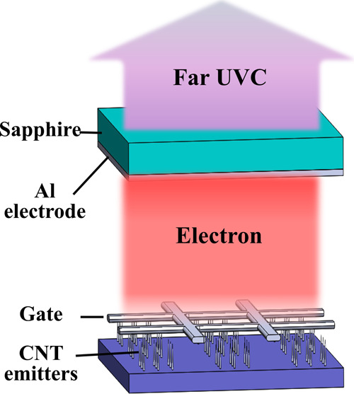
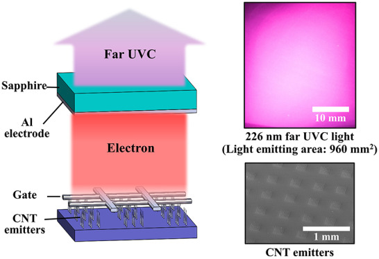
Schematic of far UVC light generation with the sapphire wafer and C-beam pumping. The anode consists of the sapphire wafer and an Al electrode used as an anode electrode. The CNT emitters are precisely patterned on the Si wafer, and a bias is applied to the gate to emit electrons. The emitted electrons are accelerated by the anode bias applied to the Al electrode, and the accelerated electrons collide with the sapphire wafer to generate far UVC light through the excitation and relaxation processes.
Several studies have been conducted on the light emission characteristics of Al2O3. Cathodoluminescence (CL) studies using electron beam (EB) excitation have been performed for Al2O3 powders and crystalline phases limited to α-, γ-, δ-, and θ-Al2O.15,16 Al2O3 powders of these phases showed near 7.6 eV (163 nm, VUV) and 4.5 eV (276 nm, UVC) emission through the CL analysis. Among many phases of Al2O3, such as α-, γ-, δ-, η-, θ-, κ-, and χ-Al2O3, we focused on κ-Al2O3. This is because the direct band gap of κ-Al2O3 was found to be 5.4 eV at the Γ point.17 The light generation efficiency depend on the band structure of light-emitting layers, and a direct bandgap is better than an indirect one. Therefore, we could generate 226 nm far UVC light by exciting κ-Al2O3 on a sapphire wafer.
To apprehend the relationship between the crystalline structures of the sapphire wafer, we performed X-ray diffraction (XRD) analysis with three types of sapphire wafers (Figure 2). The crystal structure of κ-Al2O3 was confirmed in all sapphire wafers (JCPDS 04-0878).17,18 However, it can be seen that the peak intensities differ for the three samples. Sample 1 has the highest XRD peak intensity, and sample 3 has the lowest one. In order to examine the effect of XRD peak intensity on UV performance, a carbon nanotube (CNT)-based cold cathode EB (C-beam) pumping technique was used to emit electrons using CNT emitters.
Figure 2.
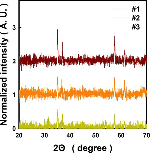
XRD results with various sapphire wafers. XRD spectra of three different sapphire wafers. The crystal structure of κ-Al2O3 was confirmed in all sapphire wafers (JCPDS 04-0878).
EB-pumped UV light sources have been researched and developed over the last 10 years.4,19−26 In 2009, Watanabe et al. explored EB pumping on hexagonal boron nitride powder to obtain far UVC light with a wavelength of 225 nm and a power conversion efficiency (PCE) of 0.6%.19 This PCE with the EB pumping technique is higher than 0.2%, which is the external quantum efficiency of UVC-LEDs at wavelengths of 226 and 227 nm.5,13 Oto et al. reported an EB pumping technique in 2010 using AlGaN MQWs with an optical output power of 100 mW and a PCE of 40% at a wavelength of 238 nm.20 In 2016, the Palo Alto Group achieved an optical output power of 230 mW at a wavelength of 246 nm using the EB pumping technology and AlGaN MQWs.21 We have also found that Zn2SiO4 pumped with the C-beam, that is, via CNT emitters as an electron source, obtained far UVC light at wavelengths of 208, 226, and 244 nm and that CNT emitters could be used as excitation sources to generate far UVC light.22 Recently, we developed 278.7 nm UVC light with AlGaN MQWs and C-beam irradiation.23 We obtained UVC lighting with a large area of 303 mm2. Based on the previous UVC generation technique through C-beam irradiation, we have developed a novel 226 nm far UVC lighting technique with high-performance C-beam excitation on a sapphire wafer.
Results and Discussion
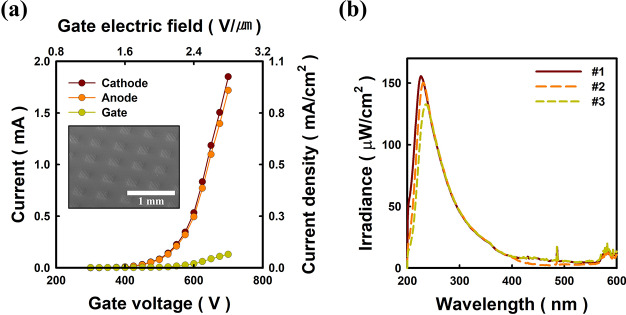
The C-beam source consists of three parts such as an anode with sapphire, a gate for electron extraction, and a cathode with CNT emitters. The electrons generated by the gate bias would pass through the gate holes and collide with the sapphire, generating far UVC light through the excitation and relaxation processes. Fully vertical aligned cone-shaped CNT emitters are arranged periodically at 30 μm intervals to enhance the electron emission current (Figure 3a). The one island consists of 49 CNT emitters in the square shape (Figure S1, Supporting Information). These islands are patterned at 0.5 mm intervals to reduce cathode current leakage through the gate electrode. The penetration ratio of the cathode electrons through the gate electrode is called as the electron transmission ratio. The higher the electron transmission ratio, the better for vacuum devices. We achieved an electron transmission ratio of 92.9% (Figure 3a). The C-beam exhibits an anode current (Ia) of 1.72 mA at a gate bias voltage (Vg) of 700 V applied at a fixed anode bias (Va) of 10 kV.
Figure 3.
(a) Electron emission characteristics of C-beam pumping. The electrons emitted by the well organizing patterned CNT emitters transmit the gate with an electron transmission ratio of 92.9% (inset: the SEM image of CNT emitters). (b) UV spectra of three different sapphire wafers with C-beam pumping. The peak intensity depends on the used sapphire wafers. The lower the peak intensity of the XRD results, the weaker the peak irradiance of the UV spectra and the red shift of the peak wavelength occurs. Far UVC light generation with C-beam pumping is affected by the crystalline quality of the sapphire wafer.
The UV spectra are obtained by making an Al electrode on three different sapphire wafers and then irradiating the C-beam (Figure 3b). To excite the sapphire anode, we input a Va of 10 kV and Ia of 1.3 mA into the Al electrode by C-beam pumping. UVC lighting performance in sample 1 indicates the highest peak irradiance and the shorted peak wavelength of 226 nm. Sample 3 shows that the peak irradiance of the UV spectrum is weak and a red shift of the peak wavelength occurs. From these results, we confirmed that the crystalline quality of the κ-Al2O3 phase is the most important for the short wavelength and high irradiance of UVC lighting by C-beam irradiation.
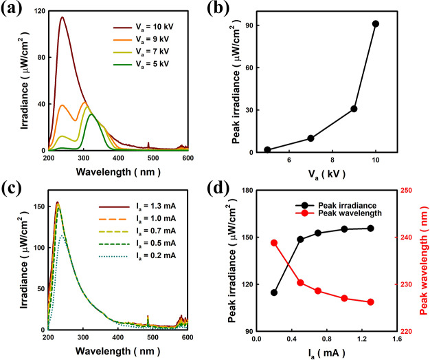
The far UVC light generation depends on the performance of electron emission characteristics and C-beam irradiation conditions. We investigated UVC generation characteristics with various irradiation conditions. UVC lighting with various Va was studied with Ia of 0.2 mA (Figure 4a). When Va was less than 9 kV, a double peak UV spectrum was observed. However, when Va was increased to 10 kV, one peak UVC spectrum with a peak wavelength of 239 nm was obtained. UV irradiance at the short wavelength increased with increasing Va (Figure 4b). In addition, small electron current at the anode is not sufficient to obtain far UVC light less than 230 nm wavelength. When Va is smaller than 9 kV, a broad peak near the UVB range is the main UV emission source in the sapphire anode, which is due to structural defects associated with oxygen vacancies.27 Thus, it was understood that more than a Va of 10 kV is needed for far UVC lighting. After fixing Va at 10 kV, we investigated the effect of Ia on the far UVC lighting performance (Figure 4c). The irradiance of the UVB range associated with the oxygen vacancies does not change, which means that the defect-related UV emission is not dependent on Ia. Irradiance and the peak wavelength of the far UVC region depend on Ia. As Ia increases to 1.3 mA, the peak irradiance increases, and the peak wavelength decreases (Figure 4d). The increment in peak irradiance decreases with increasing current and saturates at a peak wavelength of 226 nm. The peak wavelength of 226 nm is similar to the direct band gap (5.4 eV) of κ-Al2O3,17 and the peak irradiance is 156 μW/cm2 at Va of 10 kV and Ia of 1.3 mA.
Figure 4.
UV spectra with electron emission characteristics of C-beam pumping. (a) UV spectra of different Va. As the Va increases, the intensity of the peak in the far UVC region increases. (b) As Va increases, the peak irradiance at 226 nm increases. Va affects the peak irradiance of the UVC region. (c) UV spectra of different Ia. At Va of 10 kV, the main peak wavelength decreases and the peak irradiance tends to increase. (d) Peak irradiance increases, and the peak wavelength decreases with Ia increases up to 1.3 mA.
One of the most important characteristics of far UVC, generated by irradiating a C-beam onto a sapphire wafer, is the visualization of UV lighting. The sapphire wafer can emit visible light by the photoluminescence (PL) mechanism. Visible light emission by UV light induced PL in Al2O3 bulk and nano-size powders was reported by Trinkler et al.28 According to them, visible light depends on the excitation wavelength of UV light. Figure 5a,b show visible light emission images with peak wavelengths of 323 and 226 nm, respectively. A bluish-violet color is observed at a wavelength of 323 nm when Va of 5 kV and Ia of 0.2 mA are injected (Figure 5a). As Va and Ia increase to 10 kV and 1.3 mA, respectively, reddish white light is emitted (Figure 5b). The color depends on the input power of the Al electrode, and the high-power input shortens the wavelength of UVC light. Visible light emission images with various input power for 1.0, 1.4, 2.0, and 13 W are shown (Figure 5c). The visible color image changes from bluish-violet to reddish-white. As the peak wavelength decreases, the light changes from blue to violet and red to reddish-white. Visible lighting does not depend on the window materials (Figure S2, Supporting Information). For far UVC emission, we used a quartz window with a thickness of 5 mm. To confirm the origin of visible lighting, we used a glass window but nothing changed in visible light. Thus, we conclude that visible light emission comes from the PL in the sapphire wafer. We used a 430 μm thick sapphire wafer, but the electrons were able to penetrate less than 10 μm at a Va below 10 kV.20,21,25 The sapphire layer, where electrons do not reach, would make PL by the UV generated by the C-beam.
Figure 5.
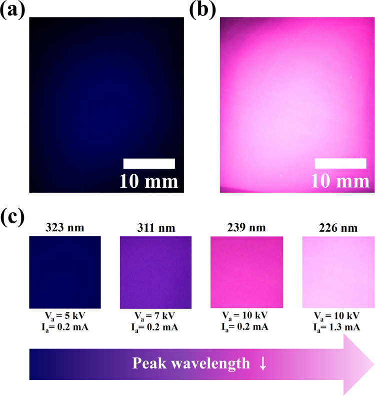
Visible light emission images generated on a sapphire wafer by C-beam pumping. (a) Input power of 1.0 W with Va = 5 kV and Ia = 0.2 mA. (b) Input power of 13 W with Va = 10 kV and Ia = 1.3 mA. (c) UV emission characteristics depend on the C-beam pumping conditions and can be easily confirmed by the color change of the optical image.
The UVC light-emitting area (A) was analyzed with an image analysis program (ImageJ program) and then obtained 960 mm2. This area would be the largest 226 nm far UVC lighting. Also, PCE was calculated by eq 1.
| 1 |
The total irradiance (E) is the sum of the peak irradiance in the UV range from 200 to 400 nm, and E is 11.8 mW/cm2 at a Va of 10 kV and Ia of 1.3 mA. Then, we obtained a PCE of 0.87% and an optical output power of 113.3 mW. This PCE of 0.87% would be higher than any UVC-LEDs and conventional EB pumping UVC light sources at wavelengths below 230 nm (Figure S3, Supporting Information).
Conclusions
In summary, the sapphire wafer and C-beam pumping technique generated far UVC light with a peak wavelength of 226 nm. At a Va of 10 kV and Ia of 1.3 mA, far UVC light with a peak wavelength of 226 nm had a light-emitting area of 960 mm2, a PCE of 0.87%, and an optical output power of 113.3 mW. UV-C emission by the C-beam irradiated on a 430 μm thick sapphire wafer can be visualized as reddish-white light at a wavelength of 226 nm. In addition, when the C-beam is irradiated the sapphire wafer, it was confirmed that the peak wavelengths of UV light were changed by the input power, and these could be easily observed by the eye. This work suggests that the sapphire wafer and C-beam pumping technique generate short wavelengths of far UVC light and can be applied to far UVC light sources with high efficiency, large emitting areas, and simple manufacturing processes.
Experimental Section
Fabrication of CNT Emitters
CNT emitters were grown on the Si wafer in a region 188 mm2 using direct current plasma-enhanced chemical vapor deposition (DC-PECVD) incorporating the mesh electrode.29 Nickel, used as the catalyst, was first deposited on a Si wafer by sputtering and was 20 nm thick. A photoresist was patterned on the Ni layer to make CNT emitters at desired positions through photolithography, and the Ni catalysts were etched using a Ni etchant.30 After that, CNT emitters were grown by DC-PECVD with a mesh grid and the substrate holder electrode for the strong positive and negative bias, respectively. The total gas pressure during growth was kept at 1.8 Torr with ammonia (NH3) and acetylene (C2H2) gas being fed. The growth time of the CNT emitters was 95 min. CNT emitters on Si wafers were grown conically and were examined using a scanning electron microscope (SEM; Hitachi S-4700) after growth.
Analysis of Sapphire
Three sapphire wafers were prepared and Panalytical X′pert Pro XRD measurements were used to analyze the crystal structure. The working voltage was 45 kV, and current was 40 mA. It was measured from 20 to 70° in the 2θ range. After XRD analysis, the anode electrode for C-beam pumping was fabricated by aluminium (Al) thermal evaporation on sapphire.
Optical Measurement
We used a UV spectrometer of Avanspec-ULS2048 (Avantes) to measure irradiance and obtain UV spectra. This spectrometer was calibrated using a UV deuterium–halogen light source. UVC light was measured at a distance of 5 mm from the sapphire wafer to the spectrometer. To generate the far UVC light, power supply and current measurements were performed on the C-beam and anode electrode using Agilent 34401A, Keithley 248, and Spellman SL1200 systems.
Acknowledgments
This work was supported by the BK21 Plus Program (future-oriented innovative brain raising type, 21A20130000018) funded by the Ministry of Education (MOE, Korea) and the National Research Foundation of Korea (NRF).
Supporting Information Available
The Supporting Information is available free of charge at https://pubs.acs.org/doi/10.1021/acsomega.0c01824.
SEM images of CNT emitters; photographs with different window materials; and PCE comparison of UVC light sources (PDF)
The authors declare no competing financial interest.
Supplementary Material
References
- Welch D.; Buonanno M.; Grilj V.; Shuryak I.; Crickmore C.; Bigelow A. W.; Randers-Pehrson G.; Johnson G. W.; Brenner D. J. Far-UVC Light: A New Tool to Control the Spread of Airborne-Mediated Microbial Diseases. Sci. Rep. 2018, 8, 2752. 10.1038/s41598-018-21058-w. [DOI] [PMC free article] [PubMed] [Google Scholar]
- Buonanno M.; Ponnaiya B.; Welch D.; Stanislauskas M.; Randers-Pehrson G.; Smilenov L.; Lowy F. D.; Owens D. M.; Brenner D. J. Germicidal Efficacy and Mammalian Skin Safety of 222-nm UV Light. Radiat. Res. 2017, 187, 493–501. 10.1667/rr0010cc.1. [DOI] [PMC free article] [PubMed] [Google Scholar]
- Kneissl M.; Seong T.-Y.; Han J.; Amano H. The Emergence and Prospects of Deep-Ultraviolet Light-Emitting Diode Technologies. Nat. Photonics 2019, 13, 233–244. 10.1038/s41566-019-0359-9. [DOI] [Google Scholar]
- Li D.; Jiang K.; Sun X.; Guo C. AlGaN Photonics: Recent Advances in Materials and Ultraviolet Devices. Adv. Opt. Photonics 2018, 10, 43. 10.1364/aop.10.000043. [DOI] [Google Scholar]
- Hirayama H.; Fujikawa S.; Noguchi N.; Norimatsu J.; Takano T.; Tsubaki K.; Kamata N. 222-282 nm AlGaN and InAlGaN-Based Deep-UV LEDs Fabricated on High-Quality AlN on Sapphire. Phys. Status Solidi A 2009, 206, 1176–1182. 10.1002/pssa.200880961. [DOI] [Google Scholar]
- Shatalov M.; Sun W.; Lunev A.; Hu X.; Dobrinsky A.; Bilenko Y.; Yang J.; Shur M.; Gaska R.; Moe C.; et al. AlGaN Deep-Ultraviolet Light-Emitting Diodes with External Quantum Efficiency above 10%. Appl. Phys. Express 2012, 5, 082101. 10.1143/apex.5.082101. [DOI] [Google Scholar]
- Takano T.; Mino T.; Sakai J.; Noguchi N.; Tsubaki K.; Hirayama H. Deep-Ultraviolet Light-Emitting Diodes with External Quantum Efficiency Higher than 20% at 275 nm Achieved by Improving Light-Extraction Efficiency. Appl. Phys. Express 2017, 10, 031002. 10.7567/apex.10.031002. [DOI] [Google Scholar]
- Grandusky J. R.; Chen J.; Gibb S. R.; Mendrick M. C.; Moe C. G.; Rodak L.; Garrett G. A.; Wraback M.; Schowalter L. J. 270 nm Pseudomorphic Ultraviolet Light-Emitting Diodes with Over 60 mW Continuous Wave Output Power. Appl. Phys. Express 2013, 6, 032101. 10.7567/apex.6.032101. [DOI] [Google Scholar]
- Mehnke F.; Kuhn C.; Guttmann M.; Reich C.; Kolbe T.; Kueller V.; Knauer A.; Lapeyrade M.; Einfeldt S.; Rass J.; et al. Efficient charge carrier injection into sub-250 nm AlGaN multiple quantum well light emitting diodes. Appl. Phys. Lett. 2014, 105, 051113. 10.1063/1.4892883. [DOI] [Google Scholar]
- Hirayama H.; Tsukada Y.; Maeda T.; Kamata N. Marked Enhancement in the Efficiency of Deep-Ultraviolet AlGaN Light-Emitting Diodes by Using a Multiquantum-Barrier Electron Blocking Layer. Appl. Phys. Express 2010, 3, 031002. 10.1143/apex.3.031002. [DOI] [Google Scholar]
- Kneissl M.; Kolbe T.; Chua C.; Kueller V.; Lobo N.; Stellmach J.; Knauer A.; Rodriguez H.; Einfeldt S.; Yang Z.; et al. Advances in Group III-Nitride-Based Deep UV Light-Emitting Diode Technology. Semicond. Sci. Technol. 2010, 26, 014036. 10.1088/0268-1242/26/1/014036. [DOI] [Google Scholar]
- Inoue S.-i.; Tamari N.; Taniguchi M. 150 mW deep-ultraviolet light-emitting diodes with large-area AlN nanophotonic light-extraction structure emitting at 265 nm. Appl. Phys. Lett. 2017, 110, 141106. 10.1063/1.4978855. [DOI] [Google Scholar]
- Liu D.; Cho S. J.; Park J.; Gong J.; Seo J.-H.; Dalmau R.; Zhao D.; Kim K.; Kim M.; Kalapala A. R. K.; et al. 226 nm AlGaN/AlN UV LEDs using p-type Si for hole injection and UV reflection. Appl. Phys. Lett. 2018, 113, 011111. 10.1063/1.5038044. [DOI] [Google Scholar]
- Kinoshita T.; Obata T.; Nagashima T.; Yanagi H.; Moody B.; Mita S.; Inoue S.-i.; Kumagai Y.; Koukitu A.; Sitar Z. Performance and Reliability of Deep-Ultraviolet Light-Emitting Diodes Fabricated on AlN Substrates Prepared by Hydride Vapor Phase Epitaxy. Appl. Phys. Express 2013, 6, 092103. 10.7567/apex.6.092103. [DOI] [Google Scholar]
- Oja M.; Feldbach E.; Kotlov A.; Mändar H.; Vielhauer S.; Kirm M. Intrinsic and Extrinsic Luminescence of Nanosize Transition Alumina Powders. Radiat. Meas. 2013, 56, 411. 10.1016/j.radmeas.2013.01.067. [DOI] [Google Scholar]
- Oja M.; Feldbach E.; Kirm M. Relaxation of Intrinsic and Extrinsic Electronic Excitations in Nano- and Micro-Size Alumina. Opt. Mater. 2019, 91, 120–125. 10.1016/j.optmat.2019.02.045. [DOI] [Google Scholar]
- Holm B.; Ahuja R.; Yourdshahyan Y.; Johansson B.; Lundqvist B. I. Elastic and Optical Properties of α- and κ-Al2O3. Phys. Rev. B: Condens. Matter Mater. Phys. 1999, 59, 12777. 10.1103/physrevb.59.12777. [DOI] [Google Scholar]
- Choi J.; Zhang S.; Hill J. M. Reducibility and Toluenehydrogenation Activity of Nickel Catalysts Supported on γ-Al2O3 and κ-Al2O3. Catal. Sci. Technol. 2012, 2, 179–186. 10.1039/c1cy00301a. [DOI] [Google Scholar]
- Watanabe K.; Taniguchi T.; Niiyama T.; Miya K.; Taniguchi M. Far-Ultraviolet Plane-Emission Handheld Device Based on Hexagonal Boron Nitride. Nat. Photonics 2009, 3, 591–594. 10.1038/nphoton.2009.167. [DOI] [Google Scholar]
- Oto T.; Banal R. G.; Kataoka K.; Funato M.; Kawakami Y. 100 mW Deep-Ultraviolet Emission from Aluminium-Nitride-Based Quantum Wells Pumped by an Electron Beam. Nat. Photonics 2010, 4, 767–770. 10.1038/nphoton.2010.220. [DOI] [Google Scholar]
- Tabataba-Vakili F.; Wunderer T.; Kneissl M.; Yang Z.; Teepe M.; Batres M.; Feneberg M.; Vancil B.; Johnson N. M. Dominance of Radiative Recombination from Electron-Beam-Pumped Deep-UV AlGaN Multi-Quantum-Well Heterostructures. Appl. Phys. Lett. 2016, 109, 181105. 10.1063/1.4967220. [DOI] [Google Scholar]
- Yoo S. T.; Hong J. H.; Kang J. S.; Park K. C. Deep-Ultraviolet Light Source with a Carbon Nanotube Cold-Cathode Electron Beam. J. Vac. Sci. Technol., B: Nanotechnol. Microelectron.: Mater., Process., Meas., Phenom. 2018, 36, 02C103. 10.1116/1.5004621. [DOI] [Google Scholar]
- Yoo S. T.; So B.; Lee H. I.; Nam O.; Chang Park K. Large Area Deep Ultraviolet Light of Al0.47Ga0.53N/Al0.56Ga0.44N Multi Quantum Well with Carbon Nanotube Electron Beam Pumping. AIP Adv. 2019, 9, 075104. 10.1063/1.5109956. [DOI] [Google Scholar]
- Ivanov S. V.; Jmerik V. N.; Nechaev D. V.; Kozlovsky V. I.; Tiberi M. D. E-Beam Pumped Mid-UV Sources Based on MBE-Grown AlGaN MQW. Phys. Status Solidi A 2015, 212, 1011. 10.1002/pssa.201431756. [DOI] [Google Scholar]
- Matsumoto T.; Iwayama S.; Saito T.; Kawakami Y.; Kubo F.; Amano H. Handheld Deep Ultraviolet Emission Device Based on Aluminum Nitride Quantum Wells and Graphene Nanoneedle Field Emitters. Opt. Express 2012, 20, 24320. 10.1364/oe.20.024320. [DOI] [PubMed] [Google Scholar]
- Jmerik V. N.; Nechaev D. V.; Toropov A. A.; Evropeitsev E. A.; Kozlovsky V. I.; Martovitsky V. P.; Rouvimov S.; Ivanov S. V. High-Efficiency Electron-Beam-Pumped Sub-240-nm Ultraviolet Emitters Based on Ultra-Thin GaN/AlN Multiple Quantum Wells Grown by Plasma-Assisted Molecular-Beam Epitaxy on c-Al2O3. Appl. Phys. Express 2018, 11, 091003. 10.7567/apex.11.091003. [DOI] [Google Scholar]
- Museur L.; Bouslama M.; Amamra M.; Kanaev A. Electronic transitions in α, θ and γ polymorphs of ultraporous monolithic alumina. Phys. Status Solidi RRL 2013, 7, 1026–1029. 10.1002/pssr.201308040. [DOI] [Google Scholar]
- Trinkler L.; Berzina B.; Jakimovica D.; Grabis J.; Steins I. UV-Light Induced Luminescence Processes in Al2O3 Bulk and Nanosize Powders. Opt. Mater. 2010, 32, 789–795. 10.1016/j.optmat.2010.01.005. [DOI] [Google Scholar]
- Lim S. H.; Park K. C.; Moon J. H.; Yoon H. S.; Pribat D.; Bonnassieux Y.; Jang J. Controlled Density of Vertically Aligned Carbon Nanotubes in a Triode Plasma Chemical Vapor Deposition System. Thin Solid Films 2006, 515, 1380–1384. 10.1016/j.tsf.2006.03.056. [DOI] [Google Scholar]
- Park K. C.; Ryu J. H.; Kim K. S.; Yu Y. Y.; Jang J. Growth of Carbon Nanotubes with Resist-Assisted Patterning Process. J. Vac. Sci. Technol., B: Nanotechnol. Microelectron.: Mater., Process., Meas., Phenom. 2007, 25, 1261. 10.1116/1.2752513. [DOI] [Google Scholar]
Associated Data
This section collects any data citations, data availability statements, or supplementary materials included in this article.


