Abstract
This article introduces in archival form the Nanolithography Toolbox, a platform-independent software package for scripted lithography pattern layout generation. The Center for Nanoscale Science and Technology (CNST) at the National Institute of Standards and Technology (NIST) developed the Nanolithography Toolbox to help users of the CNST NanoFab design devices with complex curves and aggressive critical dimensions. Using parameterized shapes as building blocks, the Nanolithography Toolbox allows users to rapidly design and layout nanoscale devices of arbitrary complexity through scripting and programming. The Toolbox offers many parameterized shapes, including structure libraries for micro- and nanoelectromechanical systems (MEMS and NEMS) and nanophotonic devices. Furthermore, the Toolbox allows users to precisely define the number of vertices for each shape or create vectorized shapes using Bezier curves. Parameterized control allows users to design smooth curves with complex shapes. The Toolbox is applicable to a broad range of design tasks in the fabrication of microscale and nanoscale devices.
Keywords: CAD, lithography, nanofabrication, nanofluidic, nanophotonic, nanoplasmonic, nanoscale curved features, nanoscale design, nanoscale devices
1. Introduction
Various lithographic processes enable patterning of structures with nanometer-scale lateral dimensions [1–12]. Lithographic nanostructures are overlaid on one another many times to fabricate the complex integrated circuit (IC) devices that make up modern semiconductor electronics. Even for simple devices, however, precise design and layout of patterns are essential. The first step in any lithographic process consists of device design. There are a number of available software packages for device design that output semiconductor-standard graphic database system II (GDSII) files, which is a binary format representing planar geometric shapes. The predominance of IC devices in manufacturing has led to the development of software packages that are ideal for designing and laying out integrated circuits, which typically have rectilinear geometries, where shape edges are parallel to the x and y axes, as Figs. 1a–c illustrates. In this scenario, every polygon is a rectangle. As a result, many of these software packages are not ideal for designing curved geometries (Fig. 1d) with aggressively-scaled dimensions for nanophotonic, nanoplasmonic, nanofluidic, and nanomechanical devices.
Fig. 1.
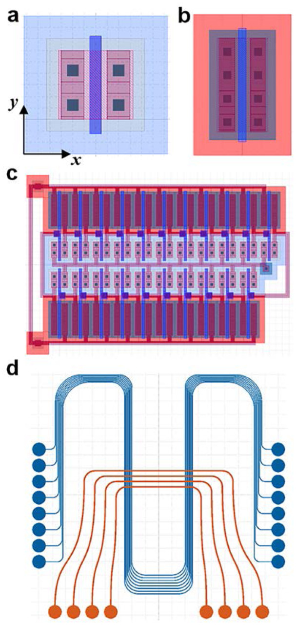
Schematic illustration of (a) n-type and (b) p-type metal oxide semiconductor (NMOS and PMOS) transistor building blocks used to create complementary MOS (CMOS) devices (c). Within CMOS architectures every polygon is a rectangle. Colors within the physical layout represent distinct lithographic levels. (d) Nanolithography Toolbox design of a microfluidic device with curved fluidic channels and ports.
Imprecise representation of curved objects at the nanoscale results in increased line-edge roughness. Scattering from the resulting edge asperities along device peripheries, for example, leads to undesirable dissipative effects in plasmonic, photonic, and other systems in which low-loss signal transmission is needed. To solve this design problem, we have developed a computer-aided design (CAD) software package for scripting and streaming complex shapes to GDSII. The Toolbox utilizes the freely available Java based (JGDS) library for encoding shapes to GDSII objects [13]. The platform-independent Nanolithography Toolbox runs on Linux1, Windows and MacOS, and is free for users to download from the Center for Nanoscale Science and Technology (CNST) website (http://www.nist.gov/cnst/). A comprehensive manual can also be found at the same address.
2. Nanolithography Toolbox Overview
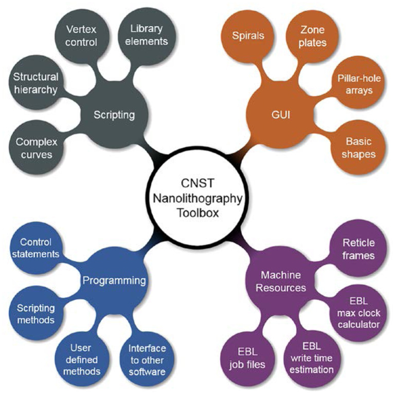
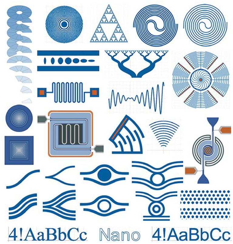
Figure 2 shows the four sections of the Nanolithography Toolbox package. The graphical user interface (GUI) allows direct export of a small subset of parameterized shapes to GDSII files. The scripting section allows full customization of device layouts with structural hierarchy, vertex control for individual shapes, and more than 400 parameterized shapes. Figure 3 shows a small subset of the available shapes, including structures from the nanophotonic and MEMS-NEMS libraries. In particular, the nanophotonic library contains a variety of microrings, S- and Y-bends based on Bezier curves, photonic crystals, tapers, spiral delay lines, grating couplers, and other complex structures. The MEMS-NEMS library includes a variety of actuators, gears, flexures, clamped beams, interacting arrays, and test and measurement structures. Since users create Toolbox scripts with text-based parameterized constructors, scripting complex structures for GDSII export does not require any programming knowledge (Appendix A).
Fig. 2.
Nanolithography Toolbox schematic illustrating the graphical user interface (GUI), scripting, programming, and machine resource sections.
Fig. 3.
Illustrative subset of parameterized shapes available for nanoscale photonic, electronic, mechanic, fluidic, and other applications.
The programming section allows for control statements and full access to scripting methods, enabling generation of custom parameterized shapes and an interface to simulation software for algorithmic design of complex nanostructures with optimal topologies. Through object-oriented programming, users can define custom methods that return a single GDSII object or a collection of GDSII objects. The Toolbox then stores the resulting shapes in GDSII structures. These platform-independent Java methods can then be reused and shared with the user community.
The machine resources section allows users to graphically create complex electron-beam lithography (EBL) job and schedule files. This is particularly useful for creating dose matrices and base dose matrices for proximity effect-corrected files [14].
3. Pattern Design
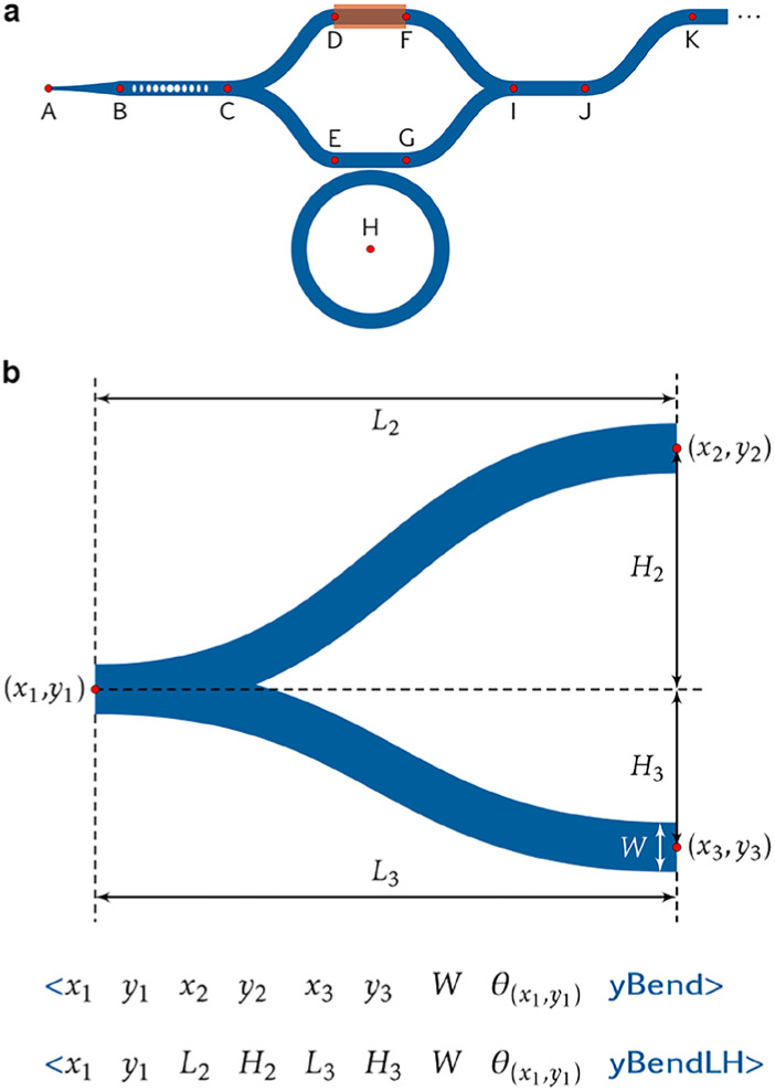
During pattern design, the design space can be viewed as a collection of grid points between which building blocks of parameterized shapes are placed. For example, Fig. 4a shows an exponential taper between points A and B, a waveguide between B and C, a y-splitter between C, D, and E, and so on. Figure 4b shows the two constructors (yBend and yBendLH) with the respective parameters used to create y-bend structures.
Fig 4.
Nanolithography Toolbox pattern layout design schematic highlighting (a) a structure composed of various available nanophotonic elements placed between grid points A through K. (b) A y-bend coupler illustrating various constructor parameters. Y-bends are made using either yBend or yBendLH scripting constructors displayed below the illustration. Y-bends of width W are defined by a start point (x1, y1), two end points and (x3, x3). Upper and lower curved segments are defined by lengths L2 and L3, and heights H2 and H3. The parameter defines object rotation about the point (x1, y1).
Precise representation of nanoscale shapes is particularly important in high-resolution EBL. Modern EBL systems have beam-position address grids with the capability for sub-nanometer grid-snapping that, in principle, enables extremely precise feature definition and edge placement. In practice, however, this capability is useful only if the device design and resulting GDSII file have similar precision. The Toolbox constructs curved shapes from a uniform vertex distribution or from vectorized shapes. In the latter case, the Toolbox constructs shapes by the concatenation of multiple cubic Bezier paths, which is more computationally efficient than the direct generation of higher-order curves. These parameterized curves allow modelling of smooth curves of arbitrary complexity. The Toolbox renders the resulting curves at the resolution limit of the EBL address grid. In general, a cubic Bezier path is defined by the following parametric equation
| (1) |
where t is a variable ranging 0 ≤ t ≤ 1, P0 and P3 are the corresponding start and end points, and P1 and P2 are the respective control points. In Cartesian coordinates Eq (1) becomes
| (2) |
| (3) |
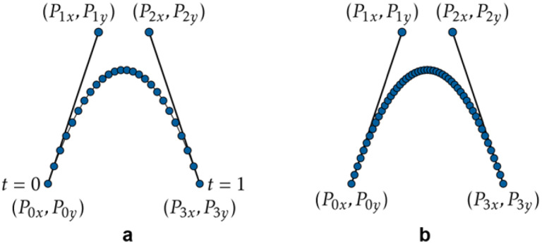
Figure 5 shows Bezier curves rendered at varying resolutions. These curves automatically exhibit an increased vertex density at higher curvatures. The points, with uniform spacing in t, become closer together in the (x, y) plane as the curvature increases. The higher density of points along curving objects allows more accurate fracturing of EBL patterns that consequently leads to smoother structures. In photonic applications, optical characteristics are highly sensitive to structural sidewall roughness profiles. Increased line-edge roughness on the nanoscale leads to a significant increase in photon propagation loss. The use of the Bezier curve approach in the Nanolithography Toolbox can eliminate sources of line-edge roughness related to pattern layout and fracturing.
Fig. 5.
Bezier curves rendered at (a) a lower and (b) a higher resolution. The blue circles along the curved path represent rendered curve vertices. Uniform distribution of t in the interval between 0 and 1 automatically yields increased vertex density at higher curvatures.
4. Impact and Future Developments
The Nanolithography Toolbox is in use by the researchers within the CNST NanoLab and by users of the CNST NanoFab. Their requirements have informed the initial development of the Toolbox, which has broadly applicable capabilities. The software will evolve over time, implementing features as the CNST identifies and prioritizes new applications.
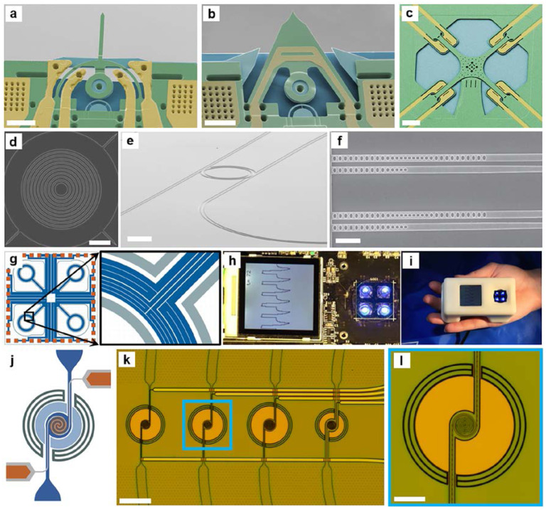
Several research projects have successfully used the Toolbox, with applications ranging from the physical to the life sciences [15–24]. Figure 6 shows representative devices from several projects that have used the Toolbox. Figures 6a–c show an on-chip cavity optomechanical transducer platform that offers high measurement-bandwidth coupled with a displacement noise-floor below 10 fm/√Hz for mechanical devices with stiffness values ranging from ≈ 0.2 N/m to ≈ 200 N/m. Integrated microdisc optical cavities allow optical measurement of micromechanical device motion. The electrothermal and electrostatic actuation allows for tuning of the readout gain. Figures 6d–f show a variety of nanophotonic and optomechanical devices designed using the Toolbox photonics library. Figures 6g–i show a hand-held, real-time Polymerase Chain Reaction (rtPCR) system capable of performing four simultaneous reactions. The system includes electronics, optics, and MEMS and is capable of detecting a single deoxyribonucleic acid (DNA) molecule. Figures 6j–l show surface micromachined, suspended fluidic channels with integrated spiral delay-line heaters. These suspended, high quality-factor, fluidic resonant-structures have applications as biological sensing platforms.
Fig. 6.
Representative devices designed using the Nanolithography Toolbox. Scanning electron micrographs (SEMs) of a MEMS cantilever with an optomechanical readout and integrated (a) electrostatic fringe-field actuation and (b) thermal bimorph actuation. (c) SEMs of silicon nitride membrane with high mechanical quality-factor and optomechanical readout (below the membrane) and integrated electrostatic fringe-field actuation. Scale bars are (a) and (b) 10 μm and (c) 20 μm. (d) SEM of a circular grating geometry used to efficiently extract light emitted from an embedded quantum dot. (e) SEM of a microring resonator add/drop device that operates as an octave-spanning optical frequency comb. (f) SEM of two optomechanical crystal devices. Each consists of a pair of nanobeams, in which the top nanobeam uses a series of etched air holes to simultaneously confine 2.4 GHz phonons and 1550 nm photons, while the bottom nanobeam acts as an optical waveguide with a left-end mirror. Scale bars are (d) 2 μm, (e) 20 μm, and (f) 2 μm. (g) Schematic design of the thermally isolated MEMS cantilever beams with integrated heaters. (h) rtPCR system with four virtual reaction-chambers and a liquid crystal display showing several amplification cycles. (i) Assembled, hand-held rtPCR device within a 3D-printed package. (j) Schematic design of a suspended fluidic channel with integrated spiral delay-line heaters. Optical micrographs of (k) an array of devices and (l) a magnified single flow-cell device. Scale bars are (k) 100 μm and (l) 30 μm.
5. Conclusions
The Nanolithography Toolbox is a platform-independent software package that is free for download and use. The CNST developed the Toolbox to help users of the CNST NanoFab to design their nanoscale devices, particularly those with curved features and small dimensions. The Toolbox offers design features that are difficult to implement in software optimized for IC design, and allows users to rapidly customize nanoscale shapes of arbitrary complexity. The Nanolithography Toolbox offers hundreds of parameterized shapes that are useful in a variety of applications spanning nanoscale photonics, mechanics, fluidics, electronics, and other disparate fields of scientific endeavor. Furthermore, the Toolbox allows users to precisely define the number of vertices for each shape or to create vectorized shapes using Bezier curves. In the former case, the Toolbox constructs the resulting shapes with a uniform vertex distribution along the periphery, rendering symmetric objects. A shape-rendering parameter controls the number of vertices for vectorized objects. The parameter is set globally for all shapes, or individually for each shape. In the latter case, the resulting rendered shapes have an increased vertex density at higher curvatures. A full description of the all the capabilities of the Toolbox can be found in the manual [25].
Acknowledgments
K.C.B., K. G., Q. L., C. B. W. and I. J. G. acknowledge support under the Cooperative Research Agreement between the University of Maryland and the National Institute of Standards and Technology Center for Nanoscale Science and Technology, award number 70ANB10H193, through the University of Maryland.
Biography
About the authors: Krishna C. Balram is a Postdoctoral Researcher at the Center for Nanoscale Science and Technology at NIST and at the Maryland Nanocenter at the University of Maryland. Daron A. Westly is a Research Scientist at the Center for Nanoscale Science and Technology at NIST. Marcelo Davanço is a Research Scientist at the Center for Nanoscale Science and Technology at NIST. Karen Grutter is a Postdoctoral Researcher at the Center for Nanoscale Science and Technology at NIST and at the Maryland Nanocenter at the University of Maryland. Qing Li is a Postdoctoral Researcher at the Center for Nanoscale Science and Technology at NIST and at the Maryland Nanocenter at the University of Maryland. Thomas Michels is a Graduate Student Researcher at the Center for Nanoscale Science and Technology at NIST and at the Ilmenau University of Technology. Christopher H. Ray is a Process Engineer at the Center for Nanoscale Science and Technology at NIST. Liya Yu is a Process Engineer at the Center for Nanoscale Science and Technology at NIST. Richard Kasica is a Process Engineer at the Center for Nanoscale Science and Technology at NIST. Christopher B. Wallin is a Postdoctoral Researcher at the Center for Nanoscale Science and Technology at NIST and at the Maryland Nanocenter at the University of Maryland. Ian J. Gilbert is a Postdoctoral Researcher at the Center for Nanoscale Science and Technology at NIST and at the Maryland Nanocenter at the University of Maryland. Brian A. Bryce is an Assistant Professor of Engineering at Harvey Mudd. Gregory Simelgor is a Senior Process Development Engineer at Edico Genome. Juraj Topolancik is a Senior Engineer at Roche Sequencing Solutions. Nicolae Lobontiu is a Professor Mechanical Engineering at University of Alaska. Yuxiang Liu is an Assistant Professor of Mechanical Engineering at Worcester Polytechnic Institute. Pavel Neuzil is a Professor at Central European Institute of Technology at Brno University of Technology and at the Department of Microsystems, Northwestern Polytechnical University, Xi’an, P.R. China. Vojtech Svatos is a Graduate Student at Central European Institute of Technology at Brno University of Technology. Kristen A. Dill is a Visual Information Specialist for the Center for Nanoscale Science and Technology at NIST. Neal Bertrand is an IT Specialist for the Center for Nanoscale Science and Technology at NIST. Meredith Metzler is a Thin Film Area Manager at the Quattrone Nanofabrication Facility at University of Pennsylvania. Gerald Lopez is a Lithography Manager at the Quattrone Nanofabrication Facility at University of Pennsylvania. David A. Czaplewski is a Scientist at the Center for Nanoscale Materials at Argonne National Laboratory. Leonidas Ocola is a Physicist at the Center for Nanoscale Materials at Argonne National Laboratory. Kartik Srinivasan is a Project Leader at the Center for Nanoscale Science and Technology at NIST. Samuel Stavis is a Project Leader at the Center for Nanoscale Science and Technology at NIST. Vladimir Aksyuk is a Project Leader at the Center for Nanoscale Science and Technology at NIST. J. Alexander Liddle is a Group Leader at the Center for Nanoscale Science and Technology at NIST. Slava Krylov is a Professor and the Head of School of Mechanical Engineering atTel Aviv University. B. Robert Ilic is a Project Leader at the Center for Nanoscale Science and Technology at NIST. The National Institute of Standards and Technology is an agency of the U.S. Department of Commerce.
6. Appendix A – Scripting Example
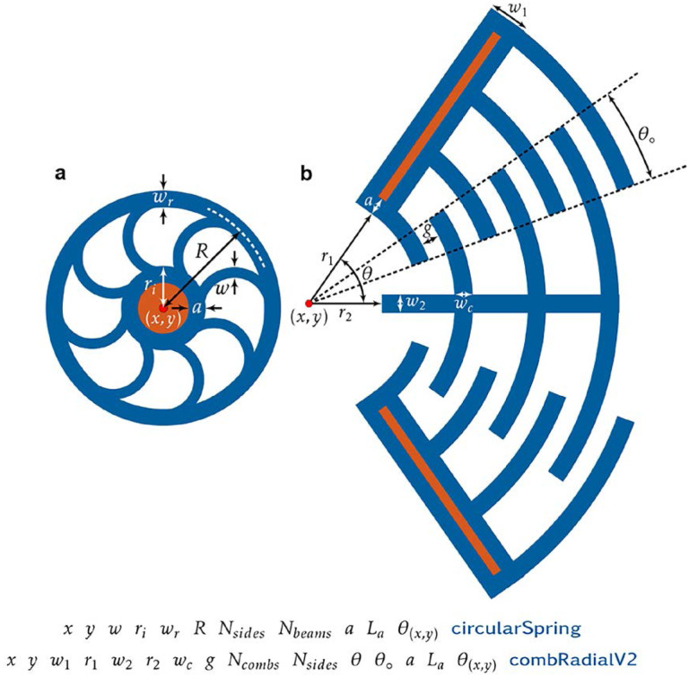
The following example illustrates the construction of a microelectromechanical actuator composed of four radial combs connected to a circular spring. Figure 7 shows a schematic illustration and constructors of the circular spring and radial combs. The circular spring is defined by the center coordinate (x, y), spring width w, inner hub radius ri, ring width wr, radius R, number of sides for the circular objects Nsides, number of circular beams Nbeams, distance from the hub edge to the anchor a, anchor GDS layer La, rotation about the center coordinates θ(x, y), and the constructor circularSpring. The radial comb is defined by the center coordinate (x, y), widths w1) and w2 and respective radial distance r1 and r2, comb width wc, gap between combs g, number of combs Ncombs, number of sides for the curved combs Nsides, opening angle theta θ, comb overlap angle θo, distance from the edge to the anchor a, anchor GDS layer La, rotation about the center coordinate θ(x, y), and constructor combRadialV2. Constructor parameter units of length and angle are expressed in micrometers and degrees, respectively.
Fig. 7.
Schematic illustration of (a) a concentric hub with circular springs and (b) a radial comb drive structures. Parameters within the schematic are defined in the respective constructors below.
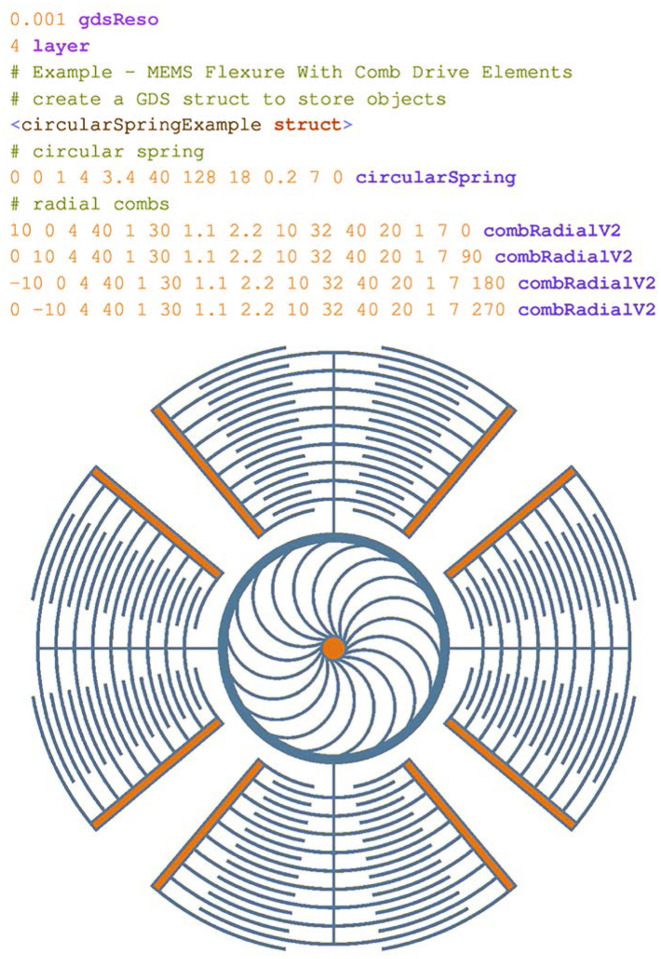
Figure 8 shows the syntax-highlighted script and the rendered GDS output of a MEMS circular spring connected to four radial comb drive elements. The script first defines the GDS rendering resolution of 0.001 nm. The next line defines GDS layer 4 for subsequent shapes. Scripting comments are denoted by # (lines 3, 4, 6 and 8). Line 5 defines a GDS structure cicrularSpringExample for storing shapes. Line 7 creates a circular spring structure with parameters defined by the circularSpring constructor (Fig. 7). Lines 9 through 12 define the connecting 4 radial combs placed at θ(x, y) = 0, 90, 180, and 270 using the combRadialV2 constructor.
Fig. 8.
Syntax-colored scripting example and the GDS rendered output of a circular spring connected to four radial comb drive elements.
Footnotes
Certain commercial equipment, instruments, or materials are identified in this paper to foster understanding. Such identification does not imply recommendation or endorsement by the National Institute of Standards and Technology, nor does it imply that the materials or equipment identified are necessarily the best available for the purpose.
7. References
- [1].Isaacson M, Murray A (1981) Insitu Vaporization of Very Low-Molecular Weight Resists Using 1–2 Nm Diameter Electron-Beams. J Vac Sci Technol 19(4):1117–1120. 10.1116/1.571180 [DOI] [Google Scholar]
- [2].Chou SY, Krauss PR (1997) Imprint lithography with sub-10 nm feature size and high throughput. Microelectronic Engineering 35(1):237–240. 10.1016/S0167-9317(96)00097-4 [DOI] [Google Scholar]
- [3].Guillorn MA, Carr DW, Tiberio RC, Greenbaum E, & Simpson ML (2000) Fabrication of dissimilar metal electrodes with nanometer interelectrode distance for molecular electronic device characterization. Journal of Vacuum Science & Technology B 18(3):1177–1181. 10.1116/1.591355 [DOI] [Google Scholar]
- [4].Yasin S, Hasko DG, Ahmed H (2001) Fabrication of <5 nm width lines in poly(methylmethacrylate) resist using a water:isopropyl alcohol developer and ultrasonically-assisted development. Appl Phys Lett 78(18):2760–2762. 10.1063/1.1369615 [DOI] [Google Scholar]
- [5].Word MJ, Adesida I, & Berger PR (2003) Nanometer-period gratings in hydrogen silsesquioxane fabricated by electron beam lithography. Journal of Vacuum Science & Technology B 21(6):L12–L15. 10.1116/1.1629711 [DOI] [Google Scholar]
- [6].An L, Zheng Y, Li K, Luo P, & Wu Y (2005) Nanometer metal line fabrication using a ZEP520∕50K PMMA bilayer resist by e-beam lithography. Journal of Vacuum Science & Technology B 23(4):1603–1606. 10.1116/1.1978893 [DOI] [Google Scholar]
- [7].Baek I-B, Yang J-H, Cho W-J, Ahn C-G, Im K, & Lee S (2005) Electron beam lithography patterning of sub-10nm line using hydrogen silsesquioxane for nanoscale device applications. Journal of Vacuum Science & Technology B 23(6):3120–3123. 10.1116/1.2132328 [DOI] [Google Scholar]
- [8].Chao W, Harteneck BD, Liddle JA, Anderson EH, & Attwood DT (2005) Soft X-ray microscopy at a spatial resolution better than 15 nm. Nature 435(7046):1210–1213. 10.1038/nature03719 [DOI] [PubMed] [Google Scholar]
- [9].Grigorescu AE, van der Krogt MC, Hagen CW, & Kruit P (2007) 10 nm lines and spaces written in HSQ, using electron beam lithography. Microelectronic Engineering 84(5–8):822–824. 10.1016/j.mee.2007.01.022 [DOI] [Google Scholar]
- [10].Yang JKW & Berggren KK (2007) Using high-contrast salty development of hydrogen silsesquioxane for sub-10 nm half-pitch lithography. Journal of Vacuum Science & Technology B 25(6):2025–2029. 10.1116/1.2801881 [DOI] [Google Scholar]
- [11].Pease RF & Chou SY (2008) Lithography and Other Patterning Techniques for Future Electronics. Proc IEEE 96(2):248–270. 10.1109/JPROC.2007.911853 [DOI] [Google Scholar]
- [12].Manfrinato VR, Zhang LH, Su D, Duan HG, Hobbs RG, Stach EA, & Berggren KK (2013) Resolution Limits of Electron-Beam Lithography toward the Atomic Scale. Nano Lett 13(4):1555–1558. 10.1021/nl304715p [DOI] [PubMed] [Google Scholar]
- [13].JGDS - Java GDS Library. Available at http://www.skinni.com. Accessed October 17, 2016.
- [14].Chang THP (1975) Proximity effect in electron beam lithography. J Vac Sci Technol 12(6):1271–1275. 10.1116/1.568515 [DOI] [Google Scholar]
- [15].Grutter KE, Davanço MI, & Srinivasan K (2015) Slot-mode optomechanical crystals: a versatile platform for multimode optomechanics. Optica 2(11):994–1001. 10.1364/OPTICA.2.000994 [DOI] [PMC free article] [PubMed] [Google Scholar]
- [16].Zhang R, Ti C, Davanço MI, Ren Y, Aksyuk V, Liu Y, & Srinivasan K (2015) Integrated tuning fork nanocavity optomechanical transducers with high fMQM product and stress-engineered frequency tuning. Appl Phys Lett 107(13):131110 10.1063/1.4932201 [DOI] [Google Scholar]
- [17].Sapienza L, Davanco M, Badolato A, & Srinivasan K (2015) Nanoscale optical positioning of single quantum dots for bright and pure single-photon emission. Nat Commun 6(7833). 10.1038/ncomms8833 [DOI] [PMC free article] [PubMed] [Google Scholar]
- [18].Li Q, Briles TC, Westly D, Stone J, Ilic R, Diddams S, Papp S, & Srinivasan K (2015) Octave-spanning microcavity Kerr frequency combs with harmonic dispersive-wave emission on a silicon chip Frontiers in Optics 2015, (Optical Society of America; ), p FW6C.5. 10.1364/FIO.2015.FW6C.5 [DOI] [Google Scholar]
- [19].Li Q, Davanço M, & Srinivasan K (2016) Efficient and low-noise single-photon-level frequency conversion interfaces using silicon nanophotonics. Nat Photon 10(6):406–414. 10.1038/nphoton.2016.64 [DOI] [Google Scholar]
- [20].Drake TE, Briles TC, Li Q, Westly D, Ilic BR, Stone JR, Srinivasan K, Diddams SA, & Papp SB (2016) An Octave-Bandwidth Kerr Optical Frequency Comb on a Silicon Chip Conference on Lasers and Electro-Optics, (Optical Society of America; ), p STu3Q.4. 10.1364/CLEO_SI.2016.STu3Q.4 [DOI] [Google Scholar]
- [21].Balram KC, Davanço MI, Song JD, & Srinivasan K (2016) Coherent coupling between radiofrequency, optical and acoustic waves in piezo-optomechanical circuits. Nat Photon 10(5):346–352. 10.1038/nphoton.2016.46 [DOI] [PMC free article] [PubMed] [Google Scholar]
- [22].Ahrberg CD, Ilic BR, Manz A, & Neuzil P (2016) Handheld real-time PCR device. Lab on a Chip 16(3):586–592. 10.1039/C5LC01415H [DOI] [PMC free article] [PubMed] [Google Scholar]
- [23].Abrahamsson S, Ilic R, Wisniewski J, Mehl B, Yu L, Chen L, Davanco M, Oudjedi L, Fiche J-B, Hajj B, Jin X, Pulupa J, Cho C, Mir M, El Beheiry M, Darzacq X, Nollmann M, Dahan M, Wu C, Lionnet T, Liddle JA, & Bargmann CI (2016) Multifocus microscopy with precise color multi-phase diffractive optics applied in functional neuronal imaging. Biomed Opt Express 7(3):855–869. 10.1364/BOE.7.000855 [DOI] [PMC free article] [PubMed] [Google Scholar]
- [24].Michels T, Aksyuk V (2016) Cavity optical transducer platform with integrated actuation for multiple sensing applications. In Proceedings, Solid State Sensor, Actuator and Microsystems Workshop, (Hilton Head Island, SC), pp 112–116. [Google Scholar]
- [25].Balram KC, Westly DA, Davanco M, Grutter KE, Li Q, Michels T, Ray CH, Yu L, Kasica RJ, Wallin CB, Gilbert IJ, Bryce BA, Simelgor G, Topolancik J, Lobontiu N, Liu Y, Neuzil P, Svatos V, Dill KA, Bertrand NA, Metzler MG, Lopez G, Czaplewski DA, Ocola L, Srinivasan KA, Stavis SM, Aksyuk VA, Liddle JA, Krylov S, Ilic BR (2016) The Nanolithography Toolbox (U.S. Department of Commerce, Washington, D.C.), NIST Handbook 160 10.6028/NIST.HB.160 [DOI] [PMC free article] [PubMed] [Google Scholar]


