

Abstract
During the manufacturing of printed circuit boards (PCBs) for a Flight Project, it was found that a European manufacturer was building its boards to a European standard that had no requirement for copper wrap on the vias. The amount of copper wrap that was measured on coupons from the panel containing the boards of interest was less than the amount specified in IPC-6012 Rev B, Class 3. To help determine the reliability and usability of the boards, three sets of tests and a simulation were run. The test results, along with results of simulation and destructive physical analysis, are presented in this paper. The first experiment involved subjecting coupons from the panels supplied by the European manufacturer to thermal cycling. After 17 000 cycles, the test was stopped with no failures. A second set of accelerated tests involved comparing the thermal fatigue life of test samples made from FR4 and polyimide with varying amounts of copper wrap. Again, the testing did not reveal any failures. The third test involved using interconnect stress test coupons with through-hole vias and blind vias that were subjected to elevated temperatures to accelerate fatigue failures. While there were failures, as expected, the failures were at barrel cracks. In addition to the experiments, this paper also discusses the results of finite-element analysis using simulation software that was used to model plated-through holes under thermal stress using a steady-state analysis, also showing the main failure mode was barrel cracking. The tests show that although copper wrap was sought as a better alternative to butt joints between barrel plating and copper foil layers, manufacturability remains challenging and attempts to meet the requirements often result in features that reduce the reliability of the boards. Experimental and simulation work discussed in this paper indicate that the standard requirements for copper wrap are not contributing to the overall board reliability, although it should be added that a design with a butt joint is going to be a higher risk than a reduced copper wrap design. The study further shows that procurement requirements for wrap plating thickness from Class 3 to Class 2 would pose little risk to reliability (minimum 5 μm/0.197 mil for all via types).Experimental results corroborated by modeling indicate that the stress maxima are internal to the barrels rather than at the wrap location. In fact, the existence of Cu wrap was determined to have no appreciable effect on reliability.
Keywords: Copper wrap, failure analysis, interconnect stress testing, plated through hole (PTH), printed circuit board (PCB)
I. Background
PRINTED circuit boards (PCBs) are the platform for electronic packaging upon which electronic components are formed into electronic systems. PCBs are used in a variety of electronic circuits from simple one-transistor amplifiers to large super computers. A PCB serves three main functions: 1) it provides the necessary mechanical support for the components in the circuit; 2) it provides the necessary electrical interconnections; and 3) it bears some form of legend that identifies the components it carries [1].
PCBs can be classified into three categories based on their construction and physical characteristics, namely, rigid, flexible and rigid–flex boards. Rigid circuit boards are composed of a composite layered structure in which solid copper sheets are laid down and separated with a dielectric material, which is commonly an epoxy resin system. Rigid boards represent the most widely used category, and they can be built from different materials systems. Flexible printed circuits consist of thin copper foil bonded to a thin plastic base. The third category is the rigid–flexible boards, which is a combination of rigid and flexible boards bonded together. Multilayer boards are made by a combination of the processes used for single sided boards and double-sided boards with plated through holes (PTHs). The individual internal layers, which may be single or double sided, are first etched in the same manner as single boards (after being punched and drilled for locating dowels), and then the layers are bonded together. The layers are laid up with prepregs between the etched layers on the alignment dowels and the assembly is placed in a powerful press to obtain a blank.
Initially, a light pressure is applied to close the layers together, and then the system is heated up. The full bonding pressure is applied, and the resin is cured at an elevated temperature. Once this stage is complete, the blank is ready for the outer layer processes. Early circuit boards contained one layer of copper foil adhered on to a phenolic backing [2]. The electronic parts, usually axially leaded parts, were mounted with screws. Since these were single-layer boards, there was little opportunity for traces to cross one another. The first big development was to go from a one-sided board to a two-sided board. The leads of the parts were used to connect one side of the board to the other. Where a trace had to go from one side to the other without the use of a part lead, a short wire known as a Z-wire was used. With either the part’s lead or the Z-wire, the standards required the wire to be bent over, thereby touching the trace as it left the solder pad area. During this time, it was learned how to get copper into the holes to help conduct the current along the leads of a leaded part, or Z-wire. The PTH is referred to as a via. Vias were not trusted to carry current without the addition of some form of wire being added. As vias matured, the number of layers to a PCB began to grow. In a four-layer configuration, power started to be carried solely by the vias between the board layers.
With advent of computer-aided design (CAD), designers and fabricators were able to bridge the gap from the electrical schematics to the controls involved in building the boards. With the use of CAD, higher layer count boards could be fabricated, and as the boards could handle more layers, the electronics going on the boards could be smaller, which, in turn, placed additional demands on the PCB. One of the newer tricks to make a board higher in signal density has been to make vias that no longer go through the entire board. Holes now may start on the outside of the PWB but stop somewhere inside of the board; these are known as blind vias. There are other places where a via can go between layers but never surface, and these are called buried vias. In both the cases of a blind via and a buried via, it becomes impossible to use the old technique of using a Z-wire to assure a signal is able to go from one layer to another.
One problem that has followed PCBs is thermal expansion. The typical root cause of filled PTH failures under thermal cycling is the difference in the Z-axis coefficient of thermal expansion (CTE) between the PCB material (a polymer), the material that fills the PTH, and the surrounding copper. The Z-axis of PCBs is conventionally defined as the axis parallel to the PTHs. When materials are heated, they physically expand, and when cooled, they contract. The X- and Y-axis CTEs of a PCB are constrained by the glass fiber weave and are not typically involved in PTH failures under thermal cycling. This constraint forces any expansion in the Z-axis. The Z-axis CTE values for typical PCBs are about 30 ppm/°C when below the glass transition temperature (Tg). However, this CTE value will vary based on multiple factors, including the polymer type, epoxy, and polyimide, which have significantly different Tg values, whereas the CTE value for copper is about 18 ppm/°C.
The physical expansion and contraction of the materials at different rates generates stress. The stress may be relieved by forming cracks in the copper, which may lead to an electrical intermittent or open circuit. Unfilled PTH cracks induced by thermal cycling typically occur near the middle of the PTH barrel, where the stress is highest [3]–[6]. When the PTHs are filled with polymer material, stress is also applied at the edges of the polymer fill between the copper wrap and copper cap plating layers [4], [5]. This crack initiates at this intersection and propagates horizontally away. Electrical intermittent opens or full opens are observed when the crack angles toward the board and propagates through the copper wrap and copper foil layers.
In the past, one of the accepted practices was to form a crook in the lead to allow for thermal expansion. Now without leads other solutions are needed to overcome the thermal expansion problem. Smaller parts have helped, but in space applications the material in the boards themselves has changed. The choice in the past was FR4, which has a higher coefficient of expansion than the parts, so there is a mismatch; it also has a low glass transition temperature, causing even more expansion issues as well as delamination problems. For PCBs that have to survive high temperatures, the material of choice is polyimide. FR4 however is still a common material that is used widely in the commercial world.
One of the areas that has been placed into focus in recent times has been the amount of copper that comes over the edge of a via hole and onto the layer plane. This could be on the surface layers in the case of a through hole, or it could be at the end of a buried via. Copper wrap is defined as the electrolytic hole plating, extending onto the surface from a plated via structure. In certain PCB fabrication processes a planarization process reduces the wrap thickness. The question has become how much copper wrap is needed to form a reliable via? A schematic illustration of copper wrap and a corresponding butt joint is shown in Figs. 1 and 2.
Fig. 1.

Copper wrap is the electrolytic hole plating deposition continuously extending onto the surface from a plated via structure. Schematic illustration of a wrap plating, 1—cap plating, 2—wrap plating, and 3—via fill.
Fig. 2.

Butt plating joint is a via structure of a surface interconnect termination with absence of copper wrap plating. In the schematic illustration, 1—butt joint plating, 2—via fill, and 3—cap plating.
Copper is added in multiple steps to a single PCB copper layer. The first is a copper foil that makes up the base copper of each copper layer in a PCB. This foil is etched to form the pattern of pads for components and the traces to connect them. After lamination, which joins all of the individual layers, the PTHs are drilled. The copper wrap plating includes the plating that covers the inside of PTHs. It covers the copper foil annular ring on the top and bottom PCB surfaces. The plating is continuous; thus, wrapping around the PTH shoulders and electrically connecting the top and bottom layers.
The fabrication steps relevant to the final wrap plating thickness begin with the copper wrap plating step. Current technology is more than sufficient to plate the minimum copper wrap and wrap plating thickness specified for Class 3 in IPC-6012 Rev B. After the copper is plated to a sufficient thickness, the PTHs are filled with a polymer. All polymer fill processes leave some cured polymer above the surfaces of the PCB.
A planarization step follows PTH fill and polymer cure because the PCBs must be flat for later fabrication steps. This planarization step removes excess polymer but also removes some copper wrap, reducing the wrap plating thickness. The amount of copper wrap removed during planarization is difficult to control.
II. Industry Specifications
Copper wrap plating and wrap plating thickness are dimensions specified for all filled PTHs in the IPC-6012 standard published by IPC. These dimensions are measured by preparing a cross section like the ones shown in Fig. 3. The microsections are etched to reveal the different copper layers prior to performing the wrap thickness measurements.
Fig. 3.

Copper wrap dimensions are measured after preparing microsections.
The wrap plating and thickness are defined in a graphic similar to Fig. 4. The cap plating is not considered in the wrap plating thickness measurement.
Fig. 4.

Copper wrap measurement, as shown in IPC-6012C.
In many IPC standards, including IPC-6012 Rev B, three values for a specified dimension are provided, categorized by performance classes. Classes 1, 2, and 3 represent different groups of electronics and are described in IPC-6011 Rev L, paragraph 1.2.
By definition, Class 1 represents general electronic products, which includes products suitable for applications where the major requirement is function of the completed assembly, Class 2 is dedicated service electronic products, which includes products where continued performance and extended life are required, and for which uninterrupted service is desired, but not critical. Typically, the end-use environment would not cause failures, and Class 3 represents high-reliability electronic products. Class 3, or high reliability electronic products, include products where continued high performance or performance-on-demand is critical, equipment downtime cannot be tolerated, end-use environment may be uncommonly harsh, and the equipment must function when required, such as life support or other critical systems. IPC-6012 Rev B paragraph 3.6.2.11.1, Figs. 3–13, and Table 3.2 together call out minimum wrap plating for PTHs and a minimum thickness for each class. These requirements are captured in Table I.
Fig. 13.

Top layer of IST coupon. Note provisions for four wire resistance measurements.
TABLE I.
IPC-6012 Rev. B Minimum Wrap Plating Thickness
| Class 1 | Class 2 | Class 3 | |
|---|---|---|---|
| Minimum Wrap Plating Thickness | As Agreed Between User and Supplier | 5μm [197μin or 0.2 mil] | 12μm [472μin or 0.5 mil] |
The basis for the copper wrap requirement described in Table I is unclear; however, it appears that in some comparative experiments reported in the open literature, a higher reliability was reported with copper wrap as compared to PTHs that are fabricated with a butt joint. The scenarios are illustrated in Fig. 2.
One premise for the copper wrap requirement is perhaps the perception that thicker copper requirements resulting in the wrap can be used as a safety margin against manufacturing variations that are introduced during the planarization process. Note that this planarization process is used in the wrap fabrication. Since wrap planarization can cause 0.3 mil or higher variations across a typical panel; PCB fabricators must target a higher value for the copper wrap [3]. It was further stated in literature that sufficient wrap cannot be achieved at required thickness for designs with tight line-width spacing and/or with multiple lamination/plating steps [8]–[10]. However, a review of Section 6 and other sections of the ECSS-Q-ST-70-11C: Space Product Assurance - Procurement of PCBs shows that there is no existing requirement for a minimum copper wrap thickness [11]. There are instances in literature that state a wrap that is 5.0 μm (.0002”) thick is robust, whereas a wrap of less than 5.0 μm is prone to early failure, although this study [12] does not provide specifics of board material, thermal cycling regime, or any other relevant information about context.
The requirements placed in the IPC specifications can contribute not only to a project’s inability to stay within budget and scheduled timelines but also to its ability to deliver the PCB hardware with high quality. The delays or lost build schedules are expensive, but failures are even more expensive. However, test sample nonconformances to a standard do not, in general, equate to PCB failures. In light of the lack of supporting reliability data and the requirements imposed in the IPC specifications, a process was implemented to utilize a risk-based decision to determine acceptability of nonconformances stemming from the PCB copper wrap requirements [13]. The impact of the nonconformance to standards and the resulting defects was explored and the merits of requirements were established using a series of experimental and modeling efforts that are described in the following sections.
III. Experiments
Three experiments and one computer modeling effort are described in the following section. The tests were undertaken in order to understand the effects of copper wrap thickness that did not meet the specifications. Accelerated tests on PCBs used in the Flight Project that were exhibiting copper wrap violation during structural integrity testing were the starting point. These constituted the first of the three tests that were conducted in order to understand the implication of violation in copper wrap thickness.
A. Experiment 1: Testing Flight Coupons
The structural integrity coupon evaluations determined that the boards represented by the coupons did not meet the IPC-6012B Class 3/A wrap copper requirement (minimum of 0.47 mils). The PCBs were supplied by a European manufacturer and met the European standards ECSS-Q-ST-70-11C [11] to which the boards were manufactured. When the coupons for the boards were reviewed at GSFC it was found that the copper wrap was insufficient to meet the 6012B 3/A standard that was imposed on the project at the time. A detailed examination of the original microsections as well as spare coupons that were submitted for each board/panel indicated that the wrap copper varied for top vias from 0.00 to 0.17 mils, bottom vias 0.00 to 0.29 ± 0.16 mils. A total of 16 top vias and 16 bottom vias were examined for each board/panel. Examples of the findings showing a copper wrap of 0.16 mil and another example with no copper wrap are shown in Fig. 5.
Fig. 5.

Examples of wrap copper findings. (a) Wrap copper of 0.16 mils from a microsection. (b) No wrap copper from a microsection.
The detailed examination found no evidence of poor bonding between the copper foil and plating, these boards were built to ECSS-Q-ST-70-11C, which does not address wrap copper in its specification. For the purpose of this test, the coupons that are provided at the periphery of the panel were used. An image of the test coupons is shown in Fig. 6.
Fig. 6.

(a) Image of the “D” coupon used for thermal cycling. (b) Hole pattern in the “D” coupons. There are 28 holes in total, out of which 24 are in the daisy chain and 4 at locations A1, A2, B1, and B2.
The boards consisted of ten layers which included a mix of buried vias, internal conductors, and PTH features. A schematic cross section of the ten-layer stack is shown in Fig. 7.
Fig. 7.

Schematic showing the stack-up of the ten layer board received from the European manufacturer.
Prior to accelerated temperature cycling, the test coupons were subjected to assembly process simulation where the coupons were thermally stressed using IPC TM-650 2.6.8 Test Condition C (to simulate the vapor phase soldering at +230 °C), followed by test condition A (to simulate hand soldering at +288 °C) with cooling in between. There was no rework on the flight boards, so rework was not simulated. In order to perform the ground testing and flight simulation, coupons were thermally shocked (and cycled) using IPC TM-650 2.6.7.2 Test Condition A (0 to +70 °C). This test condition was selected because it is closest to the expected ground testing and flight temperature range. The assembly simulations completed 17 765 cycles between 0 and +70 °C. Out of these, the first 1078 cycles were performed in a thermal shock chamber and the remaining cycles were performed in a conventional thermal cycling chamber. The resistances of six nets were monitored using a data-logger, with source current of 1 mA for the resistance measurements. The resistance monitoring interval was 30 s. A plot of the net resistance in ohms as a function of the time and cycle number is shown in Figs. 8 and 9. The colors in Figs. 8 and 9 refer to the resistance measurements taken on individual samples. In total, six D coupons were tested, with each coupon containing one net: two D coupons representing a single board/panel and four additional D coupons representing two additional boards/panels (two from each board/panel). These details have been added to the paper. It can be seen in the plots of resistance that the six monitored nets continued to exhibit the levels that were observed at the beginning of the temperature cycling tests.
Fig. 8.

Plot showing a snapshot of the thermal shock profile (top) and the corresponding change in resistance (bottom).
Fig. 9.

Plot showing a snapshot of the temperature cycling profile (top) and the corresponding changes in resistance (bottom).
During the temperature cycling and the thermal shock tests, intermittent changes in the resistance were observed on three of the six coupons. One of the D coupons developed spikes at cycle 386, which continued until the test setup was rewired into a thermal “cycling” chamber after 1078 cycles. No spikes were observed since the setup was rewired. An additional D coupon exhibited the resistance spikes at cycle 517, 518, and 520;however,nootherspikeshavebeenobserved.Anadditional D coupon developed resistance spikes at cycle 285. These spikes stopped after the test was stopped and the coupon probed to determine the cause of the spikes. There have been no observed trends in the absolute value of the resistance of the coupons during any of the cycling. Even though earlier probing of the test setup or the coupons could not get the spikes to occur, it appears that rewiring the test setup eliminated the intermittent resistance spikes.
B. Experiment 2: Thermal Cycling of Test Boards
While the boards in experiment 1 provide a very specific test sample, coupon and material set with specific test results, simultaneously a more general test was designed to determine the limit of where copper wrap started to fail. For the second set of tests, an outside laboratory was brought in to research copper wrap plating in typical PCBs procured by GSFC. The primary objective of this second test was to demonstrate the relationship between the wrap plating thickness dimension defined in IPC-6012 Rev B, Figs. 3–13, and thermal cycles to failure of the copper wrap plating. Test samples were exposed to simulated manufacturing followed by thermal cycling. The test sample design was based on a standardized interconnect stress testing (IST)coupon[14]–[16].As per the test laboratory, this standardized IST coupon design was chosen as the base design because it contained many PTHs connected in series. One test sample was designed with 16 copper layers and another with 22 copper layers. These layer counts and the signal and plane layer stack-up were designed similarly to typical PCBs procured by GSFC. The test comprised four sets of boards; two sets were fabricated with polyimide and two sets were glass-reinforced epoxy FR-4. Two different board layer configurations were used for each of the two materials, one with 16 copper layers, and the other with 22 copper layers. Within each set, the boards were divided into four groups with three groups having different amounts of copper wrap.
Two laminate materials were chosen. The first was Isola P95 polyimide, with the test samples constructed with individual laminate containing 106-style and 2116-style glass fabric weaves and having either 1 oz copper on both sides, 1 oz on one side and 0.5 oz on the other, or 0.5 oz on both sides. The prepreg material was Neltec N7305-3, with either one 1080- or one 2113-style glass fabric weave. The second laminate material was Isola PCL-FR-370HR, an FR-4 epoxy-based glass reinforced PCB material. These test samples were constructed with individual laminate each containing one C0040 style glass fabric weave and having either 1 oz copper on both sides, 1 oz on one side and 0.5 oz on the other, or 0.5 oz on both sides. The prepreg material was Isola PCL-FRP-370HR with a single 1080-style glass weave. The PTHs were filled for the all panels with a Taiyo THP-100 DX1 VF material.
Sixteen circuit board panels were designed and fabricated by Electro Plate Circuitry, Inc. (EPC). Each panel contained 22 test samplesand25or26A/B coupons and had a unique construction identified by a number–letter combination. The construction variables were wrap plating thickness designated by the numbers 1through 4, laminate material, and number of copper layers both designated by the letters A through D. Although controlling wrap plating thickness is difficult, an attempt was made by EPC to vary this dimension. The objective was to fabricate panels with the four different ranges listed below:
-
1)
Test Sample Groups with Designation 1: 0.0 mil
-
2)
Test Sample Groups with Designation 2: >0.0 to 0.2 mil
-
3)
Test Sample Groups with Designation 3: >0.2 to 0.5 mil
-
4)
Test Sample Groups with Designation 4: >0.5 mil to 0.7 mil
In the manufacturing process, there were some samples rejected by the board manufacturer such that in some cases there were as few as 18 boards, out of the 22 total that were manufactured. As per the board fabricator, EPC, it is difficult to fabricate to precise targets due to large variation resulting from the planarization process. Of the missing boards, the loss of boards was seen to be random in terms of the intended copper wrap thicknesses. Extra microsection coupons were fabricated to characterize panel variations, four or seven coupons were examined per panel, and eight measurements were taken per coupon, with two holes each.
The microsection procedure involved first cutting the A/B coupons perpendicular from the strip along designated lines using a table equipped with a diamond blade. While cutting, it was ensured that the cutting path is far enough away from PTHs so as not to induce damage. After sectioning, the coupons were rinsed with deionized water and then dried. The A/B coupons from each coupon strip were placed in a bake out oven where these are baked for 6–8 h at 135 °C ± 14 °C. The thermal stress tests on A/B coupons was performed as per methods described in the IPC-TM-650 2.6.8, Test Condition A. During this test, the temperature of the pot was verified before initiating the test, and after thermal stressing, ethanol was used to ultrasonically clean the coupons for approximately five minutes to remove any flux residues. The coupons were then microsectioned as per the procedures described in IPC-TM-650 2.1.1. Measurements of the amount of copper wrap were taken after the coupons were microsectioned. Four box and whisker plots, one for each desired copper wrap thickness are shown in Fig. 10 and summarized in Table II.
Fig. 10.
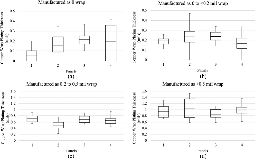
Four box and whisker plots showing the measured wrap thickness as a function of the intended wrap thickness. In this plot, panel 1 refers to the 16-layer polyimide, panel 2 refers to the 22-layer polyimide, panel 3 refers to the 16-layer FR4, and panel 4 refers to the 22-layer FR4.
TABLE II.
Average and Standard Deviation of A/B Coupon Wrap Plating Thickness
| Polyimide | FR4 | |||||||
|---|---|---|---|---|---|---|---|---|
| 16 Layer | 22 Layer | 16 Layer | 22 Layer | |||||
| A (mil) | B (mil) | C (mil) | D (mil) | |||||
| Test Samples | Avg | StDev | Avg | StDev | Avg | StDev | Avg | StDev |
| 1 (0.0inil) | 0.06 | 0.06 | 0.16 | 0.11 | 0.22 | 0.07 | 0.2 | 0.16 |
| 2 (>0.0 to 0.2mil) | 0.2 | 0.05 | 0.23 | 0.09 | 0.24 | 0.06 | 0.17 | 0.11 |
| 3 (>0.2 to 0.5mil) | 0.95 | 0.19 | 0.5 | 0.14 | 0.67 | 0.12 | 0.65 | 0.12 |
| 4 (>0.5mil to 0.7mil) | 0.7 | 0.12 | 1.05 | 0.31 | 0.86 | 0.15 | 0.99 | 0.16 |
While these results shown in Fig. 10 are representative of the test samples, the wrap plating thickness varied across each panel surface, sometimes significantly. There is significant variation in the wrap thickness across each panel. The smallest observed range was 0.2 mils, and the largest was 0.94 mils. A gradient in thickness exists across the board from top to bottom and side to side, which suggests that localized variation in wrap thickness for adjacent coupons is likely minimal, while the variation from corner to corner can be large. Despite an emphasis on controlling wrap thickness, it was difficult to achieve.
Before the temperature cycling tests were started, a preconditioning process was performed to simulate typical soldering of Center electronic products and verify the electrical continuity of each test sample. The test samples were exposed to two identical reflow cycles to simulate one tin/lead (Sn/Pb) surface mount soldering profile and one Sn/Pb rework profile. A 22-layer test sample was used to profile the reflow oven and, therefore, was exposed to atleast seven reflow profiles. This sample was chosen as one that would be most likely to fail, with the minimum wrap thickness and maximum board thickness. The preconditioning reflow profile with details is shown in Fig. 11.
Fig. 11.

Reflow profile that was used to precondition the test samples. A Vitronics Soltec XPM730 seven-zone reflow system was used for the preconditioning.
A micro-ohmmeter was used in a four-wire setup to measure the resistance of the S1 circuit on each test sample. Resistance measurements were recorded at the beginning and end of the preconditioningprocesstoverifyelectricalcontinuityaftermanufacturing and before test. The test samples were then placed in a temperature chamber for a bake out. The bake out was a typical manufacturing profile with a temperature of 125 °C and bake out time of 24 h.
Test samples were then exposed to and cycled between two temperature extremes to induce failures. The initial temperature ranges and thermal cycles that were requested were representative of typical environments Goddard’s electronic products are exposed to in project lifecycles. The two temperature ranges were −10 to 50 °C and −10 to 75 °C, for a ΔT of 60 and 85 °C, respectively. Thehigh-temperaturetolerancewas−0°C,+5°C. The low-temperature tolerance was −5 °C, +0 °C. The test samples were exposed to 500 thermal cycles, defined as the period of time beginning at the ambient chamber temperature, followed by one high temperature excursion and one low-temperature excursion, and ending at the chamber ambient temperature after the low-temperature excursion. Data from the test are presented in Fig. 12 showing the thermal profiles. Two-wire resistance measurements, with common ground, were recorded every 3 min during thermal cycling using a datalogger. These measurements were used to identify breaks in electrical continuity of test samples that could then be removed from the thermal chamber and further analyzed to identify the failure location and mechanism. The temperature was recorded using thermocouples. Thermocouple readings were recorded every 20 or 30 s using a data logger.
Fig. 12.

Thermocouple Profiles showing the temperature in the low ΔT (a) chamber and high ΔT (b) thermal chambers.
The relevant failure site at the PTH shoulders was the targeted site for these tests because it is the only location expected to be affected by the wrap plating thickness. During thermal cycling, an open circuit was defined as a recorded resistance measurement greater than 2 kΩ. Cycles to failure of a sample was defined as the number of thermal cycles up to and including the first cycle during which at least one open circuit was measured and at least one open circuit was measured during both of the two following cycles. If and when a test sample failure is recorded, the test laboratory locates the failed PTH and cross sections the test sample to determine the location and morphology of the failure in the PTH.
Additional thermal cycles were requested after no failures were observed during the 500 thermal cycles. The temperature differential was increased in both thermal chambers. The low ΔT chamber was cycled at a slightly higher ΔT: 25–125 °C for a ΔT of 100 °C. The high ΔT chamber was cycled between the largest temperature extremes possible with the test setup: −55 to 125 °C for a ΔT of 180 °C. Test samples in both thermal chambers were exposed to 200 cycles of the before-stated temperature ranges.
No failures were observed during or after the first five hundred thermal cycles or after the additional two hundred cycled. The average difference of no greater than plus or minus one milliohm indicated that any measured difference was most likely from variation in applied pressure during measurement. While the pretest measurements were taken with clips, many of the posttest measurements required probes because the wires had become brittle during the test and broke during test sample removal.
C. Experiment 3: Interconnect Stress Testing
The third test, an interconnect stress testing (IST) [14]–[16], was intended to take all coupons to failure. The test was to use the IST test method, which involves passing current through a specially designed coupon to heat up the board. In an IST, dc current is applied to a test coupon, which contains a combination of heating circuits, test, and monitoring net. The dc current causes a temperature rise in the conductors present in the coupon. Thermal cycling is achieved by cycling the current on and off. IST can simulate temperatures of solder reflow (up to 260 °C) and thermal cycling from ambient to 190 °C in ambient pressure conditions. Typically, a set number of solder simulation cycles are performed followed by temperature cycles to failure. Cycles to failure provide a figure of merit for “robustness”.
In this case, there were three sets of vias on a coupon. The first set of vias went completely through the 14-layer board. The second set of vias goes half way through the coupon, ending in a blind via. Because of the manufacturing process two different sets of coupons are required for the blind vias. One set has the vias on the “Top” of the board, while the second set has the vias on the “Bottom” of the board. The third set of vias has the current path going down only one layer of the coupon, except at one place where the via goes all of the way through the board. The through hole is half way through the circuit and is used to take the current to the other side of the board where it again then goes up and down one layer. This circuit is called the “power” circuit or heating circuit, which is intended to heat the ends of the board, to balance out any end effects. A schematic showing the top surface of the IST coupon is shown in Fig. 13.
In the third experiment, three copper wrap scenarios were used: one with no wrap, one with 0.2 mil wrap, and one with the standard0.5milcopperwrap(per the requirement).The coupons were polyimide, manufactured by Viasystems. Microsectioning was performed on samples and showed that the requested dimensions had been achieved. Tests are run by thermal cycling coupons to failure or test termination (time-terminated). Failure is defined as an increase in the resistance of 10% above the original resistance of the daisy-chained vias at ambient temperature.
Prior to the start of the IST tests, the coupons were subjected to a simulated soldering condition by exposing them to a 245 °C temperature. Testing, starting with the temperatures cycling between ambient and 150 °C, was performed on six coupons. All of the failures that occurred were on the via network that traverses all the 14 layers. The earliest failure was recorded after 2001 cycles, and the longest was after 2323 cycles. No failures were reported with either the seven-layer vias, or the one-layer (power) vias. At this time, it was realized that the boards were made of polyimide and not a G-4 material as initially assumed. G-4 uses the 150 °C as the baseline test temperature, with polyimide normally being tested to 190 °C. It was then decided to run the next 36 coupons to a peak test temperature of 210 °C.
Of the 36 coupons tested at 210 °C, all had failures of the through holes. The blind hole vias had nine failures, and the power vias had only a single failure. All types of boards had cases where all of the seven-layer vias failed, and only one coupon had a one-layer via failure. Coupons that did not fail in test were terminated at 1300, 1500, or 1700 thermal cycles, respectively. Resistance was monitored continuously during testing.
The cumulative failures per type of via and copper wrap thickness were documented and are shown in Table II. Note the coupon that experienced a “power” line failure could only be cycled up to 1013 cycles. Table III shows the minimum number of cycles on a type of wrap before any failure was noted, in this case too, the coupon that experienced a “power” line or heater circuit failure could only be cycled up to 1013 cycles.
TABLE III.
Number of Failures per Type of Via and Copper Wrap Thickness
| 0.0 mil Wrap | 0.2 mil Wrap | 0.5 mil Wrap | |
|---|---|---|---|
| 14 Layer Via | 12 | 12 | 12 |
| 7 Layer Via | 4 | 6 | 0 after 1500* Cycles |
| 1 Layer Via | 0 after 1500 Cycles | 0 after 1500 Cycles | 1 |
-test was suspended
A Weibull analysis of the coupon test failures was performed. The through-hole via data were compared using normal, log-normal and Weibull distributions. Using the software, Weibull distribution provided the best statistical goodness-of-fit, after the multi-modal distributions were accounted. A comparison of the failure distributions for the through-hole via coupons is shown in Fig. 14.
Fig. 14.

Comparison of failure distributions of the IST coupons for the through-hole vias geometry.
For through-hole via, all (no-wrap, 0.2, and 0.5 mils copper wrap) exhibited multimodal distributions for cycles to failure. It was observed that the coupons with no wrap show a bimodal distribution and a likely tri-modal for the coupons manufactured with the 0.2 and 0.5 mils copper wrap. Further, comparisons between through-hole via samples showed statistically significant differences, at a 90% confidence, for cycles to failure between both early and later distributions for the no wrap and 0.2 or 0.5 mil copper wrap coupons. The Weibull shape parameters for all through-hole via failure distributions were not significantly different. For through-hole vias, cycles to failure were not significantly different between 0.2 and 0.5 mil copper wrap coupons, for either the early or later distributions. The reliability of zero copper wrap coupons is better (i.e., exhibited longer times to failure) than either 0.2 or 0.5 mils copper wrap coupons. It is important to emphasize here that these failures only occurred in the extreme test conditions that were required to induce a failure, which were well outside of any application range for GSFC’s missions. There was no statistically significant difference in lifetimes (reliabilities, or cycles to failure) between 0.2 and 0.5 mil copper wrap coupons.
In the coupons with the blind via geometry, only the 0.2 mils copper wrap coupons provided sufficient data for comparison with through-hole via coupons. The blind via samples exhibited a larger variation in cycles to failure that occurred at longer times than for copper-wrapped through-hole vias. This larger variance is consistent with general fatigue testing, which shows greater times to failure scatter in test units that are at lower stress levels. A comparison of the through-hole coupons with other blind via coupons was not performed due to the insufficient failure data among the other blind via coupons tested. Later examination with a thermal camera of the coupons could not find where the flaw was located. It is unclear if the resistance change seen was from a single via, or found across many vias.
Out of the 36 test coupons that were stressed, 6 coupons were examined by microsection. One from each type of coupon was selected for the test. Also of note is that for any wrap thickness (three types), there was always one sample from an early failure group, and one from a delayed failure group, and the selection of sectioned coupons was random. For the six sections, all have shown barrel cracks as the failure mechanism. The microsectioning suggests that the failure sites are at the copper barrel and not at the location of the copper wrap as projected. Representative images of the three cases: no-wrap, 0.2-mil and the 0.5-mil, are shown in Fig. 15. The arrows in the microsectioned images shown in Fig. 15 point to the crack tips at the PTHs. Cracks appear to be caused by fatigue, induced due to the differential in CTE between the organic PCB material and the copper barrel.
Fig. 15.

Representative images of the three cases, no-wrap, 0.2 mil, and the 0.5 mil showing cracks in the copper plated barrel of the PTH.
D. Finite-Element Modeling
In conjunction with the physical testing on the IST coupons, a finite-element analysis was adopted, which helped in supplementing the test results. Using the COMSOL Multiphysics software, PTHs were modeled under thermal stress conditions. A steady-state analysis was used, applying a 190 °C boundary condition to the ambient article. Three vias were simulated in COMSOL. They were to simulate a fourteen-layer polyimide laminate with an epoxy material. The COMSOL modeling assumed no defects.
A single PTH surrounded by laminate was created as the model geometry. This was considered to be the worst-case condition, as the heated laminate would expand locally around the PTH without constraint from mounting fixtures or any adjacent PTHs. Opting to use a single PTH, as opposed to an array of vias, also significantly reduced the FEA computation time. Given that this simulation is a parallel to experimental testing performed on PCB coupons, the geometry of the finite-element article correlates to the previously discussed IST coupons from the ICESat-2 GPS receivers. These are 14-layer polyimide boards fabricated to IPC-6012B Class 3/A quality criteria. The geometry was defined in accordance with the design drawing, fabrication notes, and coupon microsection report (minimum observed values). Table IV lists the geometry parameters, with dimensions as defined in Fig. 16.
TABLE IV.
Minimum Cycles to a Failure
| 0.0 mil Wrap | 0.2 mil Wrap | 0.5 mil Wrap | |
|---|---|---|---|
| 14 Layer Via | 259 | 135 | 128 |
| 7 Layer Via | 448 | 372 | 0 after 1500* Cycles |
| 1 Layer Via | 0 after 1500 Cycles | 0 after 1500 Cycles | 1013 |
-test was suspended
Fig. 16.

Sketch showing the geometry variables as defined in the virtual cross section.
This study was evaluated in a three-dimensional (3-D) space to allow for orthotropic material definition and to account for the multiaxial interactions occurring with thermal expansion. The PTH was modeled by defining a two-dimensional (2-D) work plane for a quartile of the cross section, which was mirrored over the XY plane and rotated 360° to create the 3-D hole structure. The PTH was then surrounded by a block of dielectric to represent the PCB test article (dielectric may be virtually hidden in some of the figures so as to not obscure the PTH).
The material properties were defined in accordance with manufacturer data sheets and literature [17]–[30], as summarized in Table V. The laminates and via fill materials were selected based on historical usage in NASA GSFC flight PCBs. The mix includes different laminate blends including polyimides, FR-4, and ceramic materials. The Taiyo THP-100DX1 VF via fill is electrically non-conductive, while the DuPont CB100 fill is conductive, lending to sufficiently differing characteristics for this analysis.
TABLE V.
Geometry Definitions for Finite-Element Analysis
| Parameter | Variable | Value [in] | Source |
|---|---|---|---|
| Board layers | layers | 14 | Design |
| Board stack-up | t_stackup | 0.124 | Calculated from below parameters |
| Dielectric thickness | t_dielectric | 0.0076 | Microsection |
| Hole diameter | hole_diameter | 0.012 | Design (nominal value) |
| Cap plating thickness | t_cap | 0.003 | Microsection |
| Wrap plating thickness | t_wrap | 0.0005 | IPC-6012B 3/A |
| Barrel plating thickness | t_barrel | 0.0017 | Microsection |
| External foil thickness | t_extfoil | 0.0007 | Microsection |
| Internal foil thickness | t_intfoil | 0.0014 | Microsection |
| Annular ring/pad size | EAR | 0.0155*8 | Design, 20% reduction per IPC-6012B 3/A |
| Etchback | etchback | 0.00035 | Microsection |
The thermal physics of this simulation replicated the accelerated life test environment as per the IST methodology by which the ICESat-2 coupon samples were stressed. A 210 °C boundary temperature was applied to the exposed surfaces at the top and bottom of the virtual PCB, while the entire volume was given an initial temperature at ambient conditions. In the model, the temperature boundary acts as an infinite heat source at a prescribed temperature, and the simulation resolves when the volume reaches thermal equilibrium at the applied temperature. To address the structural mechanics, the PCB was constrained at a fixed position along its sides. This provides a datum for the calculations while still allowing the PCB to locally expand around the PTH without constraint. Finally, a mesh was applied, with the outer PCB dielectric being coarser than the finer areas around the PTH, shown in Fig. 17. This allows a higher resolution in the computations around the areas of interest and accounts for the very small geometry at the via interfaces.
Fig. 17.

Model mesh with the outer PCB dielectric being coarser than the finer areas around the PTH.
The thermal expansion physics in the finite-element software was used to couple the structural mechanics and heat transfer modules, outputting physical deformation as a function of the temperature and relevant material properties. Simulations were run for the following conditions:
-
1)
Baseline configuration replicating the ICESat-2 GPS Receiver boards (Isola P95 laminate, Taiyo THP via fill, typical copper properties, and 0.5 mils of copper wrap)
-
2)
Baseline materials with variable wrap thickness: 0.6, 0.4, 0.2, and 0 mils (where the zero-mil option represents a butt joint)
-
3)
Baseline wrap and materials, with variable electroplated copper properties (elastic modulus and Poisson’s ratio)
-
4)
Baseline wrap and copper materials, with variable mix of laminates and via fills
In order to assess the mechanical damage in the model, the finite-element software computed von Mises stress was first considered as the failure criterion to be used. However, upon review, the stress values were much higher than expected; in the baseline model configuration, the maximum stress in the barrel was computed at ~252 000 psi, while the ultimate tensile strength of electroplated copper is just ~40 000 psi. If the computation were accurate, the experimentally tested coupons would have seen many infant mortalities, but in reality, the coupons failed in fatigue after many cycles. The error in the COMSOL-calculated stress is hypothesized to be caused by ignoring plastic deformation in the copper. Assuming perfect elastic deformation results in inaccurate stresses above the yield strength of the material, where the stress-strain curve becomes nonlinear. Given this inaccuracy in the stress relationship in the material definition, the computed strain will instead be used for the risk analysis of fatigue failures. This is expanded in the risk analysis section of this paper. However, the von Mises stress plots are still considered here to visualize the local stress concentrations within the PTH and identify the likely failure sites and mechanisms. Thus, the scale of the stress must be ignored in this section, and instead the relative magnitude will be reviewed to contribute to the risk analysis.
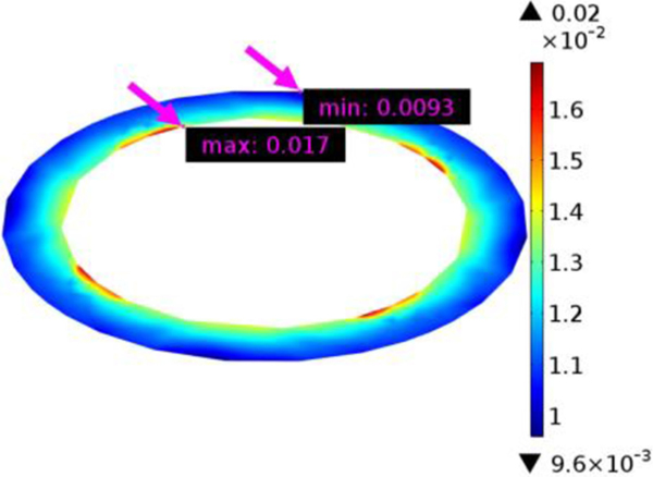
Note that, unless otherwise specified, the graphics in this section are for the baseline simulation case (Isola P95 laminate, Taiyo THP via fill, original electroplated copper properties, and 0.5 mils of copper wrap). Fig. 18 shows a model cross section along the center of the PTH. At this extended glance, the stress appears higher towards the center of the PCB. This correlates well with the experimental failure analyses, which showed barrel cracks forming at the central layers of the coupons.
Fig. 18.

COMSOL-calculated von Mises stress [psi] plotted on the cross section for baseline case.
Upon closer inspection at the center of the hole, as seen in Fig. 19, the maximum stress in the entire model cross section is observed within the barrel.
Fig. 19.

COMSOL-calculated von Mises stress [psi] maximum near center of the PCB for baseline case.
These stress concentrations shown in Fig. 19 correspond to the presence of the internal annular rings. FEA analysis shows a stress concentration that appears around the etchback region where the annular ring protrudes into the barrel. This observation confirms other studies [34], [35] where the effects of positive etchback are examined. It is learned, from these studies, that there is a long-held belief that positive etchback is better for long-term reliability than a simple desmear. The results of these studies show that desmear as a hole wall preparation process can result in a 20% improvement over the slight positive etchback condition, and they further indicate that slightly positive etchback condition can result in a 40% improvement over the excessive positive etchback condition, a condition which is only 0.0005” greater than the slight positive condition, and is still well within the upper limit of industry etchback specifications. Both of these locations in the barrel are represented in failure analysis photos from the IST experiments, as seen in Fig. 20.
Fig. 20.

Failure analysis microsection from ICESat-2 IST coupons showing barrel cracks formed at the via center along the barrel and at the etchback locations.
At the knee of the hole, a local stress concentration is observed at the intersection of the via fill, cap plating, and via barrel, as shown in Fig. 21.
Fig. 21.

COMSOL-calculated von Mises stress [psi] at copper wrap location for baseline case.
An overview plot of the strain in the cross section may be seen in Fig. 22. The via fill experiences the greatest expansion, as the peak temperature in the test exceeds the Tg of the fill materials.
Fig. 22.

Strain plotted on the model cross section.
The strain results were compiled for the various test cases simulated, as well as for the volumes or interfaces of interest as plotted in the subsequent figures, as shown in Table VI. These results are further discussed in the risk analysis section (see Figs. 23, 24, 25, 26, 27, 28, and 29).
TABLE VI.
Material Definitions for Laminates, Via Fills, and Copper
| Tg [°C] |
α1/α2 [ppm/°C] |
Cp [J/gK] |
ρ [lb/in3] |
k [W/mK] |
E [ksi] | λ | |
|---|---|---|---|---|---|---|---|
| Laminate | |||||||
| Isola P95 | 260 | {13,14,55} | 0.95 | 0.058 | 0.2 | 3892 | 0.187 |
| Arlon 85N | 250 | {16,16,55}/{16,16,149} | 0.94 | 0.058 | 0.2 | 3200 | 0.15 |
| Nelco N7000-2 HT | 260 | 10 | 1.06 | 0.061 | 0.45 | 3100 | 0.146 |
| Rogers R04350B | 280 | {10,12,32} | 0.9 | 0.067 | 0.69 | 2432 | 0.4 |
| Duroid 6002 | N/A | {16,16,24} | 0.93 | 0.076 | 0.6 | 120 | 0.4 |
| Isola HR370 | 180 | {13,14,45}/{14,17,230} | 0.94 | 0.058 | 0.4 | 3744 | 0.177 |
| Via Fill | |||||||
| Taiyo THP-100DX1 VF | 155 | 32/81 | 900 | 0.059 | 0.58 | 652.67 | 0.34 |
| DuPont CB100 | 115 | 27/47.2 | 309 | 0.2 | 3.5 | 2000 | 0.34 |
| Copper | |||||||
| Copper foil | N/A | 17.7 | 385 | 0.32 | 391 | 17000 | 0.35 |
| Electroplated copper | N/A | 17.7 | 385 | 0.32 | 401 | 18850 | 0.34 |
Tg = glass transition temperature, α1/α2 = coefficient of thermal expansion (CTE) below/above Tg, Cp = specific heat capacity at constant pressure, ρ = density, k = thermal conductivity, E = elastic modulus, λ = Poisson’s ratio
Fig. 23.

Sketch showing the virtual domain evaluated as the copper wrap volume.
Fig. 24.

Strain plotted on the 3-D wrap volume for baseline case.
Fig. 25.
Strain plotted on the 2-D via barrel to cap plating interface for the butt joint model.
Fig. 26.

Strain plotted on 3-D via barrel volume for baseline case.
Fig. 27.

Location defined as the vertical edge of the external foil where crack can separate the foil from the barrel.
Fig. 28.

Strain plotted on 2-D interface at the vertical edge of the external foil for the baseline case.
Fig. 29.

Coffin-Manson cyclic strain vs. fatigue life plot for electrodeposited copper (IPC-TR-579).
The computed strain did not vary significantly between the different wrap thickness conditions. The strain was even very slightly less for the case of the butt joint. A conclusion is drawn that the wrap geometry itself, be it thickness or use of a butt joint, does not affect the strain damage. However, a difference persists in the failure mechanism, given that copper wrap will fail cohesively as a crack through the wrap, as opposed to the Butt joint, which will fail adhesively along the bond line between the cap plating and top of the barrel. In this, an experimental determination would need to be made quantifying the strength of the electroplated bond versus the tensile strength of the material in order to actually compare the relative likelihood of a copper wrap vs. butt joint failure (see Table VII).
TABLE VII.
Compilation of Simulation Results for Maximum Strains
| Wrap Thickness Sweep | ||||
|---|---|---|---|---|
| Wrap Thickness [in] | Barrel Strain | Wrap Strain | Wrap Edge Strain | |
| 0.0006 | 0.017 | 0.019 | 0.012 | |
| 0.0004 | 0.017 | 0.021 | 0.012 | |
| 0.0002 | 0.017 | 0.019 | 0.012 | |
| 0 | 0.017 | 0.017* | 0.012 | |
| Electroplated Copper Property Sweep | ||||
| Elastic Modulus [ksi] | Poisson’s Ratio | Barrel Strain | Wrap Strain | Wrap Edge Strain |
| E=18855 | λ = 0.34 | 0.017 | 0.020 | 0.012 |
| E+10%=20740 | 0.017 | 0.020 | 0.013 | |
| E−10%=16969 | 0.016 | 0.020 | 0.012 | |
| E=18855 | λ+10%=0.374 | 0.016 | 0.019 | 0.012 |
| λ−10%=0.306 | 0.017 | 0.021 | 0.013 | |
| Laminate and Via Fill Material Mix | ||||
| Laminate | Via Fill | Barrel Strain | Wrap Strain | Wrap Edge Strain |
| Isola P95 | Taiyo THP-100DX1 VF | 0.017 | 0.020 | 0.012 |
| DuPont CB100 | 0.015 | 0.014 | 0.012 | |
| Arlon 85N | Taiyo THP-100DX1 VF | 0.017 | 0.020 | 0.013 |
| DuPont CB100 | 0.016 | 0.014 | 0.012 | |
| Nelco N7000–2 HT | Taiyo THP- | 0.014 | 0.020 | 0.010 |
| 100DX1 VF | ||||
| DuPont CB100 | 0.013 | 0.014 | 0.010 | |
| Rogers R04350B | Taiyo THP-100DX1 VF | 0.015 | 0.020 | 0.011 |
| DuPont CB100 | 0.013 | 0.014 | 0.011 | |
| Duroid 6002 | Taiyo THP-100DX1 VF | 0.015 | 0.020 | 0.012 |
| DuPont CB100 | 0.015 | 0.014 | 0.012 | |
| Isola HR370 | Taiyo THP-100DX1 VF | 0.045 | 0.021 | 0.022 |
| DuPont CB100 | 0.046 | 0.021 | 0.022 | |
Given no wrap, this is the strain value at the via barrel to cap plating interface as depicted in Figure 25.
Slight variations in the copper material properties (see Table VIII) did not present significant changes to the resultant strains. The effects of the laminate and via fill thermal expansion mismatch, expanded upon below, changed the results far more significantly.
TABLE VIII.
Maximum Strains for Variable Wrap Thickness
| Wrap Thickness Sweep | |||
|---|---|---|---|
| Wrap Thickness [in] | Barrel Strain | Wrap Strain | Wrap Edge Strain |
| 0.0006 | 0.017 | 0.019 | 0.012 |
| 0.0004 | 0.017 | 0.021 | 0.012 |
| 0.0002 | 0.017 | 0.019 | 0.012 |
| 0 | 0.017 | 0.017* | 0.012 |
Given no wrap, this is the strain value at the via barrel to cap plating interlace as depicted in Figure 25.
The polyimide laminates—Isola P95, Arlon 85N. and Nelco N7000–2 HT—as well as the ceramic laminates—Rogers 04350B and Duroid 6002—all had very similar results with maximum strains around l%−2% in the areas of interest. The largest difference was seen in the FR-4 laminate, the Isola HR370, which showed higher strains at all locations, notably a maximum barrel strain around 4.5%. This is attributed to the laminate’s lower glass transition temperature at 180 °C—the only laminate Tg that is surpassed by the 210 °C boundary temperature. The Z-axis expansion jumps from 45 to 230 ppm/°C post-Tg, as compared to the 17.7 ppm/°C CTE of the copper. In this highly accelerated test simulation, the Isola HR370 presents the greatest relative risk for fatigue failure, but in reality, the material would be suitable for most use environments (i.e., not at extreme temperatures).
Comparing the via fills, the Taiyo THP-100DX1 VF presented slightly higher strains than the DuPont CB100 material. While the Taiyo fill has a higher Tg at 155 °C compared to the DuPont’s 115 °C, the post-Tg CTE is nearly double (81 versus 47.2 ppm/°C). Further, the elastic modulus of the DuPont material is over triple that of the Taiyo. Again, for most use environments these fills would perform similarly; these differences are exacerbated in this study given the high-temperature environment.
Of the properties studied in this simulation, the laminate and fill material selection will have the greatest impact on the risk for fatigue failures in PTHs. To mitigate the risk, high reliability materials should be used that have lower expansion rates and a glass transition temperature well above the expected use environment.
To validate the model against the test data, a prediction of cycles to failure may be estimated from the FEA-computed strain values. IPC-TR-579 [34] presents an equation and graphical representation of a Coffin-Manson cyclic strain life, originally developed by Engelmaier and Kessler for electroplated copper in PTHs [35].
Solving this equation using the FEA-derived 2% maximum strain for the baseline case, the estimated mean cycles before failure (MCBF) is 258. To correlate this computational result to the experimental testing, the real IST samples survived five preconditioning cycles to a 245 °C peak in addition to hundreds of cycles (135–412 cycles). The PCB samples were fabricated across six different manufacturing panels with varying wrap thicknesses, however an assumption is made that the copper wrap did not affect the fatigue life. In combining the test results from the 36 IST coupons, the MCBF from all of the test samples was 222, plus the five preconditioning cycles to the higher peak temperature. Given that the experimental MCBF value is close to the theoretical value from this FEA study, the results and conclusions drawn from the relative reliability of the variables explored in this FEA model are considered valid.
Based on the results of this FEA study, the expected failure mechanism is thermal expansion-induced fatigue, given small strains that would be experienced over many thermal cycles. This notion is experimentally validated with the previous IST study, wherein the coupons of variable wrap thickness failed in a wear-out mode (barrel cracking) after preconditioning and hundreds of accelerated life cycles(135–412range,222MCBF). The model also reaffirms that the barrel is more likely to crack than the knee of the hole, given the higher stresses at the center of the hole.
Conversely, to consider the likelihood of a tensile fracture, IPC-6012B Class 3/A requires a minimum tensile elongation of 18% for electrodeposited copper plating as tested per IPC-TM-650, Method 2.4.18.1. The strain values calculated in this model are much lower, typically ~2% with the worst case at 4.6% for the Isola HR370 material reaching above its glass transition temperature. The boards would pass the IPC elongation test with significant margin. Moreover, IPC-TR-579 defines the copper fracture strain—i.e., the expected failure condition—at a much higher 30% (see Fig. 30). Thus, there is considered to be no risk of an infant mortality or failing with a single thermal expansion.
Fig. 30.

Linearized stress-strain diagram for electrodeposited copper (Su = 40 000 psi, Sy = 25 000 psi, ECu = 12 × 106 psi, = 0.1 × 10^6 psi, Df = 30%) (IPC-TR-579).
It is worth mentioning that the shortcoming of FEA and computer-based analysis is the assumption of perfect quality, while variability is intrinsic to the manufacturing process in PCBs. The conclusions in this paper do not take into account the possibility for defects such as imperfect copper bonding or separations that would lend to weak points for crack initiation and propagation. These off-nominal conditions, caused by manufacturing and workmanship issues, must be screened out with microsectioning of coupons on production lots. That said, given that the presence and thickness of copper wrap did not significantly affect the PTH mechanical integrity, copper wrap is not considered to affect PCB reliability. Material selection presents a far greater impact on the PTH life. Moreover, given that higher stresses are experienced towards the center of the hole, the PCB copper barrel is expected to fail first in a wear-out environment over the knee of the hole.
Risk mitigation controls to improve PCB reliability in a thermal environment may include:
-
1)
Select PCB materials with a high glass transition temperature and the lowest CTE, or ensure that the use environment is appropriate within the context of the material’s thermal properties.
-
2)
Ensure that appropriate measures are taken to control the PCB temperature in test and use environments (e.g., heat sinks or fans).
-
3)
Use quality controls to reduce workmanship defects and to screen out off-nominal conditions such as imperfect copper bonding or separations, which could contribute to risk.
IV. Discussion
The results from the three test sets contradict what was believed. The rationale for 0.5 mils of copper wrap was not supported. The life test (test 1) conducted by temperature cycling the sample coupons was designed to test a very specific set of boards, representative of the flight boards, that had already been fabricated for a box. The boards were to be accepted if the test showed they were robust enough to survive the flight environment, and they are. As a result, the answers obtained by the test were specific to the boards, and did not cover different wrap conditions or material sets. The thermal shock and thermal cycle testing has demonstrated that the boards meet the “physical endurance” requirements per IPC-TM-650, Method 2.6.7.2. It should be noted that at the 17 765 cycle mark (between 0 and +70 °C), the stresses are equivalent to 1776 cycles between −65 and +170 °C, which is greater than the 100 cycles called out for polyimide. The comparison of 17 765 cycles between 0 and +70 °C, and 1776 cycles between −65 and +170 °C was made using the Coffin–Manson expression (for fatigue) with an exponent of 1.9 (exponent of 1.9 came from an analysis performed by an Industry partner on test boards that were subjected to the IST test conditions). Note that the expression and exponents are for material fatigue and do not address any issues that there may be with the interfaces between the copper wrap and the base copper. So for this analysis, we are assuming that there isn’t any issue with the bond. The structural integrity coupons did not find any evidence of issues with the bond
Using this expression, cycles between −65 and +170 °C equate to approximately 1779 cycles. The expected temperature range for the flight boards was the standard 0–40 °C, with margins of ±10 °C being added for testing. While the temperature extremes are included to cover events like safehold, it is expected that the orbit-to-orbit thermal excursion will only be about 4 °C. The data provide the PCB designer with the necessary tools to establish the desired characteristics and evaluate the trade-off between fabrication processes and requirements to achieve the desired reliability, yield, and cost.
Even at this high cycle count, the resistance of the coupons was stable. However, it should be noted that the resistance of the coupons would not be expected to increase noticeably until the coupons were close to failure, i.e., no degradation is apparent prior to failure. As of this writing, destructive microsectioning has not yet been performed, but it is planned for the near future (see Tables IX and X).
TABLE IX.
Maximum Strains for Variable Electroplated Copper Properties
| Electroplated Copper Property Sweep | ||||
|---|---|---|---|---|
| Elastic Modulus [ksi] | Poisson’s Ratio | Barrel Strain | Wrap Strain | Wrap Edge Strain |
| E=18855 | λ=0.34 | 0.017 | 0.020 | 0.012 |
| E+10%=20740 | 0.017 | 0.020 | 0.013 | |
| E−10%=16969 | 0.016 | 0.020 | 0.012 | |
| E=18855 | λ+10%=0.374 | 0.016 | 0.019 | 0.012 |
| λ−10%=0.306 | 0.017 | 0.021 | 0.013 | |
TABLE X.
Maximum Strains for Variable Laminate and Via Fill Materials
| Laminate and Via Fill Material Mix | ||||
|---|---|---|---|---|
| Laminate | Via Fill | Barrel Strain | Wrap Strain | Wrap Edge Strain |
| Isola P95 | Taiyo THP-100DX1 VF | 0.017 | 0.020 | 0.012 |
| DuPont CB100 | 0.015 | 0.014 | 0.012 | |
| Arlon 85N | Taiyo THP-100DX1 VF | 0.017 | 0.020 | 0.013 |
| DuPont CB100 | 0.016 | 0.014 | 0.012 | |
| Nelco N7000-2 HT | Taiyo THP-100DX1 VF | 0.014 | 0.020 | 0.010 |
| DuPont CB100 | 0.013 | 0.014 | 0.010 | |
| Rogers R04350B | Taiyo THP-100DX1 VF | 0.015 | 0.020 | 0.011 |
| DuPont CB100 | 0.013 | 0.014 | 0.011 | |
| Duroid 6002 | Taiyo THP-100DX1 VF | 0.015 | 0.020 | 0.012 |
| DuPont CB100 | 0.015 | 0.014 | 0.012 | |
| Isola HR370 | Taiyo THP-100DX1 VF | 0.045 | 0.021 | 0.022 |
| DuPont CB100 | 0.046 | 0.021 | 0.022 | |
In the second test set, no relationship between wrap plating thickness and thermal cycles to failure was found. The testing did show that the design and materials chosen for this test, including a wide range of wrap plating thicknesses, withstand significant thermomechanical stress compared to typical environments GSFC electronic products are exposed to. If the chosen design, materials, and simulated manufacturing conditions for these test samples are representative of GSFC PCBs, the outside laboratory believes that a change in NASA GSFC PCB procurement requirements for wrap plating thickness from Class 3 to Class 2 would pose little risk to reliability. Although testing was originally going to be for 500 cycles, with the failure criterion being a coupon showing a resistance change of greater than 2 kΩ, the standard change in resistance of greater than 10% was not used in this case due to limitations in test equipment. The meter measuring the resistance throughout the test had a built in 300 Ω resistor and was built for two wire resistance measurements instead of the four-wire system needed for low resistance changes. The rationale for the 2000 Ω change was because it was expected that even a 10% change could only be caused by a crack in the copper accounting for more than 90% of the via’s width or contact area. It was believed that a 90% crack would not last much longer and an open would soon occur.
The third test set, which was the IST coupon testing was the only test in this study where failures were observed, and the test was designed to have failures. The failures that were found were all in the copper barrels, propagating as cracks, and not at the expected copper wrap location. The failures occurred in all of the through-hole vias, and a smaller number (29%) on the blind vias, and a single failure on the one-layer vias. To produce the failures seen, the temperature of the boards was elevated to a very high temperature (210 °C), which is close to the glass transition temperature of the polyimide material.
The COMSOL simulations provided additional insight and confidence in understanding the behavior of the PTH when subjected to thermal cycling that occurs during a PWB’s lifecycle. The results help to understand defect progression from defect onset to failure based on defect type, size, locations on the PCB, board dimensions, and materials used. Two finite-element models of PCB coupon (one-via model and a three-via model) were created and solved using COMSOL, a heat transfer module is used to simulate the thermal stress equivalent to the interconnect stress test (IST) for the models. The model shows that the highest von Mises stress is located in the copper barrel. The high von Mises stress can cause barrel and knee cracks. Using stress against the number of cycles to failure (S–N) curve for ultrafine-grained copper, the average number of cycles to failure for each model was estimated based on the maximum von Mises stress at a temperature ranging from 25 to 210 °C. Since the maximum von Mises stress at each temperature is only slightly different in each of the models, the average number cycles to failure is estimated to be almost the same. The results show that as the temperature increases, the average number cycles to failure decreases significantly.
V. Summary
Experimental and simulation work was performed to understand the reliability implications of the condition in the board supplied by the European PCB manufacturer, as the European spec was satisfied, but the project requirement for IPC 6012B 3/A was not met. Specifically, PCBs without copper wrap were identified during coupon inspection. Temperature cycling and thermal shock tests on coupons fabricated with polyimide and FR4 materials suggest that copper wrap thickness is not a dominant contributor to failure in PTH geometries. No failures were observed in either of the first two studies, which were performed at reasonable qualification and flight-representative conditions. Destructive physical analysis of test coupons of the third test(interconnect stress test IST), which was performed at stress levels far exceeding any reasonable qualification level, suggests that the failure sites are located in the barrels, away from the copper wrap location. The earliest failure occurred at 128 cycles at a test temperature of 210 °C. Software simulation confirms the IST test observations. Simulations show that von Mises stress concentrations are observed along the PTH barrel when elevated temperature is applied at the boundary conditions. A periodicity in the von Mises stresses suggests that the geometry and number of annular rings plays a dominant role in the stress concentration along the PTH barrel. The tests show that although copper wrap was sought as a better alternative to butt joints between barrel plating and copper foil layers, manufacturability remains challenging when targeting a minimum thickness. Experimental and simulation work discussed in this study indicates that the standard requirements for copper wrap are not contributing to overall board reliability. Although a design with a butt joint is always going to be a higher risk than even a reduced copper wrap design, the study shows that procurement requirements for wrap plating thickness from Class 3 to Class 2 would pose little risk to reliability (minimum 5 μm/0.197 mil for all via types). Experimental results corroborated by modelling indicate that the stress maxima are internal to the barrels rather than at the wrap location.
Acknowledgment
The authors would like to thank the NASA Office of Safety and Mission Assurance, Quality Program, the Reliability and Maintainability (R&M), the Goddard Materials Engineering Branch for the financial support and internal reviewers who contributed to this study. The authors would like to acknowledge Mr. Richard Barney who provided insights and expertise that greatly assisted this research.
This work was supported by the NASA Office of Safety and Mission Assurance, Quality and the Reliability and Maintainability (R&M) Programs.
Biography

Bhanu Sood(SM’14)is the Commodity Risk Assessment Engineer (CRAE) with NASA Goddard Space Flight Center, Greenbelt. He serves as the Goddard Center lead and NASA Specialist managing overall development efforts pertaining to quality and reliability of microelectronics packaging and circuit boards used in NASA Goddard’s flight missions and ground support equipment. He also serves as the NASA authority on technical Standards committees and advisory groups for PCBs and assemblies, and manages the establishment and implementation of new research, technology development, and demonstration initiatives relating to microelectronics packaging, circuit boards, and electronic circuit assemblies. Prior to joining NASA, he was the Laboratory Director of the Center for Advanced Life Cycle Engineering (CALCE), University of Maryland, College Park, MD, USA, where he provided reliability and supply chain risk assessment services to organizations from the aerospace, avionics, medical device, telecommunications, petrochemical, and automotive industries. In his prior appointment at Naval Research Laboratory (NRL), he developed processes for 3-D printing and patented a 3-D stereo-lithography technique. He holds two patents and one invention disclosure.
Mr. Sood is a member of SAE and ASM.
John Shue photograph and biography not available at the time of publication.

Jesse Leitner received the B.S. degree from the University of Texas at Austin, Austin, TX, USA, and the M.S. and Ph.D. degrees from Georgia Tech, Atlanta, GA, USA, all in aerospace engineering.
Since 2009, he has been the Chief Safety and Mission Assurance Engineer with NASA Goddard Space Flight Center, Greenbelt, MD, USA, responsible for the technical direction for NASA GSFC’s Directorate for Safety and Mission Assurance(SMA).In this role, he develops policies and procedures to ensure technical excellence and engineering integrity for SMA practices across GSFC; coordinates, recommends solutions for, and reports on problems and issues across the Center; and facilitates technical coordination for activities in engineering, SMA, and projects and programs at GSFC. He was the principal creator of the risk-based SMA organization at GSFC, including organizational structure, new positions, and a range of processes, procedures, and standards involving risk analysis and risk-based engineering approaches.

Kelly Daniluk received the B.S. degree in mechanical engineering from the University of Maryland, College Park, MD, USA.
She is currently a Reliability Engineer under the Safety and Mission Assurance (SMA) Services contract with NASA Goddard Space Flight Center (GSFC), Greenbelt, MD, USA. She supports spaceflight missions in identifying project risks and facilitating fault management. She is presently on the team for the Plankton, Aerosol, Cloud, and ocean Ecosystem (PACE) mission, which seeks to advance ocean and atmospheric science. She is also the lead analyst for finite element and physics-of-failure modeling of spaceflight electronics in GSFC Safety and Mission Assurance. Her work includes virtually qualifying new printed wiring assembly designs; assessing the risks of nonconforming workmanship conditions to validate spaceflight hardware; and conducting virtual design of experiments to contribute to industry knowledge of electronics reliability. She draws from quality engineering experience under the NASA Workmanship Standards Program, where she was a subject matter expert in printed circuit board assurance.

Lionel-Nobel Sindjui received a B.S. in mechanical engineering in 2015, and a Master of Engineering in mechanical engineering in 2018, both from the University of Maryland, College Park, MD, USA.
He is a Junior Reliability Engineer with NASA Goddard Space Flight Center (GSFC), Greenbelt, MD, USA. During his time at GSFC, he has worked to improve the printed circuit board assurance process. This includes providing finite element analysis support to simulate printed circuit board environmental conditions, researching on new developing technology in the field of electronic packaging and analyzing printed circuit board supply chain trends.
REFERENCES
- [1].Coombs CF, Coombs’ Printed Circuits Handbook. New York, NY, USA: McGraw-Hill, 2001. [Google Scholar]
- [2].Sood B. and Pecht M, Printed Circuit Board Laminates. Wiley encyclopedia of composites. New York, NY, USA: Wiley, 2012. [Google Scholar]
- [3].Goval D, Azimi H, Chong KP, and Lii MJ, “Reliability of high aspect ratio plated through holes (PTH) for advanced printed circuit board (PCB) packages,” in Proc. 35th Annu. Proc. IEEE Int. Rel. Phys. Symp, Apr. 1997, pp. 129–135. [Google Scholar]
- [4].Su F. et al. , “On thermo-mechanical reliability of plated-through-hole (PTH),” Microelectron. Rel, vol. 52, no. 6, pp. 1189–1196, 2012. [Google Scholar]
- [5].Huang SQ, Yung KC, and Sun B, “A finite element model and experimental analysis of PTH reliability in rigid-flex printed circuits using the Taguchi method,” Int. J. Fatigue, vol. 40, pp. 84–96, 2012. [Google Scholar]
- [6].Wu JH, Meng-Chieh L, Tzeng-Cherng L, and Te-Chun H, “Comparison the reliability of small plated-through hole with different diameters under thermal stress,” in Proc. 2011 6th Int. Microsyst., Packag., Assembly Circuits Technol. Conf, Oct. 2011, pp. 161–164. [Google Scholar]
- [7].Michael F. and Furlong J, “Application of reliability/survival statistics to analyze interconnect stress test data to make life predictions on complex, lead-free printed circuit board assemblies,” in Proc. EPC 2004, 2004. [Google Scholar]
- [8].Carano M, Via Hole Filling Technology for High Density, High Aspect Ratio Printed Wiring Boards Using a High Tg, Low CTE Plugging Paste. Maple Plain, MN, USA. [Google Scholar]
- [9].Park N. et al. , “Fatigue life prediction of plated through holes (PTH) under thermal cycling.” in Proc. Eur. IEEE Microelectron. Packag. Conf, 2009, pp. 1–4. [Google Scholar]
- [10].Freda M, “Via life vs. temperature stress analysis of interconnect stress test,” CircuiTree, March 2005. [Google Scholar]
- [11].European Cooperation for Space Standardization, ECSS-Q-ST-70–11C: Space Product Assurance - Procurement of Printed Circuit Boards, ESAESTEC Requirements and Standards Division, The Netherlands, 2008. [Google Scholar]
- [12].Reid P, “The wrap crack,” PCB Design Mag, p. 78, November 2012. [Google Scholar]
- [13].Leitner J. et al. , “Risk-based safety and mission assurance: Approach and experiences in practice,” Quality Eng, 2018. [Google Scholar]
- [14].Birch SM, Gavrel GM, and Memon ZI, “Interconnect stress test coupon,” U.S. Patent 5 451 885, Sep. 19, 1995.
- [15].Birch SM, Gavrel GM, and Memon ZI, “Method of manufacture of an interconnect stress test coupon,” U.S. Patent 5 701 667, Dec. 30, 1997.
- [16].Dufresne RA et al. , “Structure and method for reliability stressing of dielectrics,” U.S. Patent 5 898 706. Apr. 27, 1999.
- [17].Isola Group. (n.d.). P95/P25. [Online]. Available: https://www.everythingrf.com/products/laminates/isola-group/605-277-p95-p25
- [18].Isola Group. (n.d.). 370HR. [Online]. Available: http://www.isola-group.com/products/370HR/
- [19].Dupont.(n.d.). CB100. [Online]. Available: http://www.dupont.com/content/dam/dupont/products-and-services/electronic-and-electrical-materials/documents/prodlib/CB100.pdf
- [20].Allen Woods & Associates. (n.d.). Tatsuta AE3030 Features vs. CB100. [Online]. Available: http://allenwoodsgroup.com/pdf/TATSUTAAE3030.pdf
- [21].Park Electrochemical Corp. (n.d.). Nelco N7000–2 HT Laminate. [Online]. Available: http://www.parkelectro.com/parkelectro/images/n7000-2ht.pdf
- [22].Rogers Corporation (n.d.). RO4350B Series Circuit Materials. [Online]. Available: http://www.murrietta.com/materials/pdf/Rogers-RO4000-Data-Sheet.pdf
- [23].Rogers Corporation. (n.d.). RO3003 Series Circuit Materials. [Online]. Available: http://www.prototron.com/documents/materials/RO3000.pdf
- [24].Arlon Electronic Materials Division. (n.d.). TC600. [Online]. Available: https://imageserv11.team-logic.com/mediaLibrary/303/TC600.pdf
- [25].Arlon Electronic Materials Division. (n.d.). 85NT Polyimide Nonwoven Aramid Laminate and Prepreg. [Online]. Available: http://www.cadxservices.com/guides/pdfs/arlones55.pdf
- [26].Arlon Electronic Materials Division. (n.d.). 85N. [Online]. Available: https://imageserv11.team-logic.com/mediaLibrary/303/85N.pdf
- [27].Taiyo America Inc. (n.d.). THP-100DX1 VF. [Online]. Available: http://taiyo-america.com/docs/files/2414/6041/6490/TDS_THP-100DX1_Series_April_11_2016.pdf
- [28].Massachusetts Institute of Technology. (n.d.). Copper – PVD or Electroplated. [Online]. Available: http://www.mit.edu/~6.777/matprops/copper.htm
- [29].Coombs CF, Copper foil properties, in Printed Circuits Handbook. New York, NY, USA: McGraw-Hill, 1996. [Google Scholar]
- [30].Chang F-K, Ed., “Structural health monitoring 2013: A roadmap to intelligent structures,” in Proc. 19th Int. Workshop Structural Health Monitoring, Sep. 10–12, 2013, DEStech Publications, Inc., 2013. [Google Scholar]
- [31].IPC-6012 Qualification and Performance Specification for Rigid Printed Boards.
- [32].Reid P, “Reid on reliability: Buried via reliability,” 2011. [Online]. Available: http://pcb.iconnect007.com/index.php/article/60730/reid-on-reliability-microvia-separation/60733/?skin=flex
- [33].Furlong J. and Freda M, “Application of reliability/survival statistics to analyze interconnect stress data to make life predictions on complex, lead-free printed circuit board assemblies,” presented at EPC2004, Cologne, Germany, Oct. 5, 2004. [Google Scholar]
- [34].Tardibuono MJ, “Characterization of PCB plated-through-holes reliability using statistical analysis,” Circuit World, vol. 31, no. 1, pp. 8–15, 2005. [Google Scholar]
- [35].Trakas G, Hoeppel G, and Cai J, “Etchback and its effect on PWB Reliability,” 2018. [Online]. Available: https://www.researchgate.net/publication/237750006_Etchback_and_its_Effect_on_PWB_Reliability
- [36].IPC, “IPC-TR-579 round robin reliability evaluation of small diameter plated-through holes in printed wiring boards,” in Proc. IPC, Northbrook, 1988. [Google Scholar]
- [37].Engelmaier W. and Kessler T, “Investigation of agitation effects on electroplated copper in multilayer board plated-through holes in a forced-flow plating cell,” J. Electrochemical Soc, vol. 125, no. 1, pp. 36–43, January 1978. [Google Scholar]