

Abstract

Inspired by the unique properties of graphene, research efforts have broadened to investigations of various other two-dimensional materials with the aim of exploring their properties for future applications. Our combined experimental and theoretical study confirms the existence of a binary honeycomb structure formed by Ag and Te on Ag(111). Low-energy electron diffraction shows sharp spots which provide evidence of an undistorted AgTe layer. Band structure data obtained by angle-resolved photoelectron spectroscopy are closely reproduced by first-principles calculations, using density functional theory (DFT). This confirms the formation of a honeycomb structure with one Ag and one Te atom in the unit cell. In addition, the theoretical band structure reproduces also the finer details of the experimental bands, such as a split of one of the AgTe bands.
The research field of two-dimensional (2D) materials has attracted great attention in recent years. Such materials may have unique properties that are not present in the three-dimensional bulk. The search for 2D materials for applications in the next generation of electronic and optoelectronic devices is currently quite intense. Prominent examples are the discovery of graphene1 and subsequent investigations of single-element graphene-analogues from group IV, such as silicene, germanene, and stanene.2 Another type of 2D materials consists of high-Z (Z = atomic number) substitutional surface alloys on noble metals. Surface alloying is recognized as a viable way to achieve unique physical and chemical properties not found in the bulk. For example, a giant Rashba-type of spin splitting3 was observed for Ag2Bi,4 while the corresponding replacement of Ag by the lighter element Sb resulted in a barely observable split.5 Very recently, a 2D Sb analogue of graphene, so-called antimonene, was reported to be successfully formed on Ag(111), with a lattice constant and orientation matching a (√3 × √3)R30° supercell.6 Hence, it is very interesting and worthwhile to examine whether Te, the group VI neighbor of Sb, forms a graphene-like flat 2D honeycomb structure or a surface alloy with spin splitting on Ag(111). Actually, in this Letter, we report experimental and theoretical results that provide evidence for a combination of the two alternatives. We find that the electronic band structure matches that of a binary AgTe 2D honeycomb alloy structure.
The feasibility of forming binary honeycomb structures has been reported for a 2D layer of CuSe on Cu(111).7,8 Scanning tunneling microscopy (STM) images presented in ref (8) showed a clear honeycomb structure, and the conclusion that the unit cell consisted of one Cu and one Se atom was inferred from a comparison between experimental and calculated band structures. From the striped appearance observed in STM images, it was further concluded that the CuSe honeycomb structure was uniaxially distorted. This deviation from an ideal honeycomb structure resulted in a splitting of the CuSe spots in the low-energy electron diffraction (LEED) pattern from the CuSe layer.8 A honeycomb structure has also been reported for 2D layers of AgTe on Ag(111) in two recent studies.9,10 STM and LEED results from a sample annealed at 720 K, in ref (9), showed different structures denoted as buckled, with ridges and trenches, and striped with uniaxially elongated honeycombs. As in the case of CuSe, the various distortions of the honeycomb layer were clearly revealed by additional diffraction spots in the LEED patterns. In ref (10), STM data from a AgTe sample annealed at 500 K showed a striped structure resembling that of the striped structure discussed in ref (9). The large size of the AgTe spots in the LEED pattern in ref (10) is consistent with the presence of several unresolved spots, as expected from a distorted honeycomb layer.
In our Letter, we present data from a AgTe layer characterized by sharp LEED spots which is evidence for a well-ordered surface layer without the distortions reported in the previous studies of the binary honeycomb layers.7−10 Detailed band structure data obtained by angle-resolved photoelectron spectroscopy (ARPES) in combination with calculated band structures of various models, based on density functional theory (DFT), is used to verify the formation of a 2D AgTe honeycomb structure. Further, our ARPES data reveal a Rashba type of spin-split in the lower band of the two originating from the AgTe 2D layer.
In order to prepare the AgTe structure, presented in this Letter, a Ag(111) crystal was cleaned by repeated cycles of sputtering by Ar+ ions (1 keV) and annealing at approximately 400 °C until a sharp (1 × 1) LEED pattern was obtained. Tellurium was deposited onto the clean Ag(111) sample at room temperature from a source that was calibrated by a thickness monitor. The data were obtained from a sample prepared by depositing 1/3 monolayer (ML) of Te followed by annealing at approximately 200 °C for 5 min. After this preparation, LEED showed sharp diffraction spots from the AgTe layer corresponding to a (√3 × √3)R30° periodicity with respect to Ag(111) (see Figure 1a). The sharpness of the spots indicates an ordered structure with a well-defined periodicity without the type of distortions reported in refs (7−10). Core-level spectroscopy data from the inner shell electrons provide additional information related to the atomic structure. Figure 1b shows a high-resolution Te 4d core-level spectrum. This spectrum is accurately fitted by just one spin–orbit split component plus a linear background. The lack of shifted components indicates that the Te atoms are located at identical positions consistent with a well-ordered structure.
Figure 1.

LEED and core-level spectroscopy data. (a) LEED pattern (78 eV) of the AgTe/Ag(111) sample showing sharp diffraction spots, indicating a well-ordered structure with a (√3 × √3)R30° periodicity relative to Ag(111). One of the Ag 1 × 1 spots is indicated by a red arrow. The green arrow points at one of the spots from the AgTe layer. (b) Te 4d core-level spectrum obtained using a photon energy of 80 eV at normal emission. The black circles are the experimental data, and the fitting curve is the sum of one spin–orbit split component and a linear background. Fitting parameters: spin–orbit split, 1.47 eV; branching ratio, 0.636; Gaussian width, 387 meV; and Lorentzian width, 373 meV. The asymmetry parameter of the Doniach–Šunjić line profile is 0, which indicates a semiconducting character of the AgTe 2D structure.
The band structure of the AgTe layer, probed by ARPES, using a photon energy of 35 eV, is presented in Figure 2a,b. These data reveal a semiconducting band structure in agreement with the symmetric line shape of the Te 4d spectrum. The band dispersions follow a √3 × √3 periodicity, which is clear from the band mapping along the Γ̅K̅M̅Γ̅ and Γ̅M̅Γ̅ paths of the √3 × √3 surface Brillouin zone (SBZ), indicated in Figure 2c. From these data, one can conclude that there are two bands separated in energy and momentum space. The upper band, S1, has a maximum at a binding energy (EB) of ∼0.75 eV at Γ̅1, with respect to the Fermi level (EF). The dispersion of S1 shows a local maximum as well as a local minimum at M̅ along K̅M̅K̅ and Γ̅M̅Γ̅, respectively. This makes M̅ a saddle point with a diverging density of states (van Hove singularity). The S2 band shows a downward dispersion with a maximum EB of 1.1 eV at the center of the SBZ. In contrast to S1, the S2 band exhibits a small splitting along both Γ̅Μ̅ and Γ̅Κ̅, indicated by the black arrows in Figure 2a,b. This band split is shown more clearly in the ARPES data in Figure 3a, which was obtained with a photon energy of 26 eV around Γ̅2 along Γ̅M̅Γ̅. To further enhance the visibility of the splitting of S2, we display, in Figure 3b, the second derivative along the energy axis of the ARPES data in Figure 3a. As discussed in the literature, high-Z surface alloys on noble metal surfaces show a Rashba-type of spin splitting looking quite similar to the split of S2. The smallest, barely observable, splitting was found on the Ag2Sb surface alloy on Ag(111).5 Because the atomic number of Te is increased one step compared to Sb, one can expect to observe a spin splitting as is reported here for the AgTe honeycomb layer. The separation in momentum space of the two sub-bands of S2 for the AgTe honeycomb structure is Δk// = 0.045 ± 0.005 Å–1. This value is quite similar to the value of Δk// = 0.06 Å–1 for Ag2Pb11 but significantly smaller than Δk// = 0.26 Å–1 for the Ag2Bi4 surface alloy, which shows the largest splitting. In this context, one can note that the prototypical case of a Rashba split, i.e., the Shockley surface state on Au(111),12,13 shows a split of 0.024 Å–1.
Figure 2.

Electronic band structure of AgTe on Ag(111) obtained by ARPES. (a) Energy bands mapped along the Γ̅K̅M̅K̅Γ̅ line indicated by the green dashed line in panel c. (b) Energy bands mapped along Γ̅M̅Γ̅M̅. The photon energy was 35 eV. Two bands are indicated by S1 and S2, respectively, in panels a and b. These bands constitute the 2D band structure of AgTe on Ag(111) along the high-symmetry lines. B originates from direct transitions involving Ag sp bulk bands. UB denotes umklapp scattering of B by √3 × √3 reciprocal lattice vectors. Black arrows indicate band splittings. White arrows point to places in the band structure, where the splitting is expected, but is less clear in the data. (c) Schematic drawing of SBZs. Red hexagon shows the 1 × 1 SBZ of the Ag(111) surface. Black hexagons represent √3 × √3 SBZs of AgTe. Green dashed lines indicate the high-symmetry lines in the SBZs, along which the experimental data were obtained. Several symmetry points are marked by yellow circles.
Figure 3.
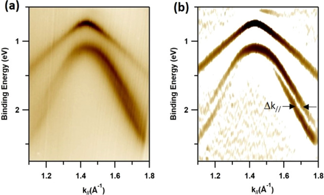
Details of the experimental band structure showing a split of the S2 band. (a) Close up of the dispersions of the S1 and S2 bands in the vicinity of Γ̅2 along Γ̅M̅Γ̅. The photon energy was 26 eV. S2 is split into two sub-bands while no split could be detected for S1. (b) Second derivative along the energy axis of the ARPES data in panel a. The resulting enhanced band structure clearly shows the splitting of S2 into two bands, which are separated along the momentum axis by Δk// = 0.045 ± 0.005 Å–1.
Based on the number of bands, the periodicity in k// space, and the line shape of the Te 4d spectrum, some more or less likely models can be envisioned. We have considered four models with a √3 × √3 supercell with respect to Ag(111). (i) Te adatoms (1/3 ML) positioned at hollow sites on the Ag(111) surface. (ii) A monolayer of graphene-like Te, i.e., tellurene. (iii) A substitutional Ag2Te surface alloy, i.e., one out of three Ag atoms in the √3 × √3 cell is substituted by Te in the upper atomic layer. (iv) An AgTe 2D binary honeycomb structure. These four models are visualized after full relaxation in Figure S1. The theoretical band structures of all four models are presented together with the experimental one in Figure S2. We find that only model iv can explain all the features observed in the ARPES data.
In the following, we present band structure calculations, which were performed based on DFT using the PAW method14 implemented in VASP.15 We employed the generalized gradient approximation (GGA) with the PBE16 exchange–correlation. Our calculated results lead to the conclusion that the AgTe layer is well-described by model iv mentioned above and shown in Figure 4a. One Te atom (blue ball) and one Ag atom (yellow ball) form a honeycomb structure with a lattice constant of 5.0 Å, which matches a √3 × √3 supercell of the Ag(111) surface. After full relaxation of the slab, described in Methods, the AgTe honeycomb structure was stable on the Ag(111) surface with very small buckling (Te atoms being 0.1 Å higher than Ag atoms). Panels b and c of Figure 4 show the results of band structure calculations, plotted along M̅Γ̅Κ̅Μ̅, without and with spin–orbit coupling, respectively. Red dots highlight px/py states of the AgTe layer. Comparing Figures 2 and 4, one finds a striking agreement between the ARPES data and the calculated band structure with spin–orbit coupling. The calculated Σ1 and Σ2 bands in Figure 4c reproduce the dispersions of S1 and S2 extremely well. There is an energy difference of ∼0.31 eV between Σ1 and Σ2 at the Γ̅ point, which closely reproduces the experimental separation of ∼0.36 eV between S1 and S2. Regarding the absolute energy positions of Σ1 and Σ2 compared to S1 and S2, we find a difference of ∼0.3 eV. A most likely reason for the deviation is that self-energy effects, to obtain the quasiparticle band structure, are not included in the present calculations.17 Another extraordinary agreement is the small but resolvable splitting of Σ2, with Δk// ≈ 0.040 Å–1, which compares closely to the experimental splitting of Δk// ≈ 0.045 Å–1. The combination of spin–orbit coupling and the broken inversion symmetry at the surface point to a split of the Rashba type of Σ2/S2. Such spin-splits have been extensively studied in the case of substitutional surface alloys, such as Ag2Pb and Ag2Bi.4,11 It is interesting to note that the calculated value of the direct band gap at Γ̅ in Figure 4c is ∼0.65 eV, which is very close to the ∼0.75 eV binding energy of S1 in Figure 2. This indicates that the Fermi level of the system is actually pinned at an energy very close to the conduction band minimum located at Γ̅.
Figure 4.
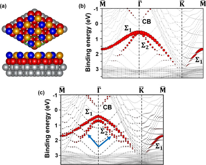
Atomic model and band structure of the AgTe honeycomb structure on Ag(111) calculated using DFT+PBE. (a) Top and side views of the atomic model. The blue balls represent Te atoms. Yellow balls represent Ag atoms which are part of the honeycomb layer. Red balls represent the first layer of the Ag(111) slab. Gray balls represent deeper Ag layers. (b and c) The calculated band structure plotted along M̅Γ̅K̅M̅, without and with spin-orbit coupling, respectively. Two valence bands from the 2D AgTe layer are labeled Σ1 and Σ2, and the conduction band is labeled CB. The blue arrows point at regions where the Σ2 band shows a small split.
A theoretical band structure including spin orbit coupling was presented along the Γ̅Κ̅ line for a honeycomb model of AgTe in ref (10). That band structure is very similar to the Γ̅Κ̅ part of Figure 4c except that the splitting in the lower band was not identified. The calculated band structure was compared to ARPES data along Γ̅Κ̅. However, the broad ARPES data could not resolve the two bands, Σ1 and Σ2, predicted by theory. Thus, the comparison with the theoretical band structure did not provide conclusive evidence to confirm the formation of a AgTe honeycomb structure in ref (10). Our detailed high-resolution ARPES data and the sharp LEED pattern from the AgTe layer provide sufficient information to verify the existence of an undistorted AgTe honeycomb layer on the Ag(111) substrate.
In summary, we have successfully grown a 2D binary AgTe honeycomb structure on Ag(111). The atomic and electronic structures were experimentally examined by LEED, core-level spectroscopy, and ARPES. The high-resolution ARPES data along the two major symmetry lines showed sufficient details to make a conclusive comparison to the calculated band structure. Not only the dispersions of the two bands (S1 and S2) but also the spin-split of the S2 band were closely reproduced by the model calculations. These results, together with the sharp LEED pattern, make a strong case for the formation of an undistorted AgTe honeycomb layer. Our results on this new type of 2D material should inspire further investigations on honeycomb structured binary alloys.
Methods
Samples were prepared in situ in an ultrahigh vacuum (UHV) system equipped with LEED and ARPES instruments. ARPES and core-level data were obtained at beamline I4 at the MAX-lab synchrotron radiation facility. The data were acquired at room temperature by a Phoibos 100 analyzer from Specs with a two-dimensional detector. The energy and angular resolutions were 50 meV and 0.3°, respectively. First-principles density functional theory (DFT) calculations were used to interpret the experimental electronic structure data from ARPES. Atomic structures were modeled by a slab, which was built from nine Ag layers terminated by a Te containing √3 × √3 supercell. Four different structures were considered (see Figure S1). About 19 Å of vacuum spacing was used to avoid interaction between neighboring slabs of the periodic structure. The positions of all atoms were fully relaxed using the functional of Perdew, Burke, and Ernzerhof (PBE) and the projector augmented wave (PAW) method including van der Waals (vdW) interaction within the Vienna ab initio simulation package (VASP) code. The energy cutoff of the plane-wave basis set was 375 eV, and the k-point mesh was (9 × 9 × 1). All atoms were relaxed until the average force was within 0.01 eV/Å. Band structure calculations were implemented considering spin–orbital coupling.
Acknowledgments
Technical support from Dr. Johan Adell, Dr. Craig Polley, and Dr. T. Balasubramanian at MAX-lab is gratefully acknowledged. Financial support was provided by the Swedish Research Council (Contract No. 621-2014-4764). The calculations were carried out at the National Supercomputer Centre (NSC) supported by the Swedish National Infrastructure for Computing (SNIC).
Supporting Information Available
The Supporting Information is available free of charge at https://pubs.acs.org/doi/10.1021/acs.jpclett.0c00123.
Atomic models referred to in the Letter, theoretical band structures of each model calculated using DFT, and comparisons to the experimental band structure obtained by ARPES (PDF)
Author Present Address
† W.W.: MAX IV Laboratory, Lund University, Box 118, SE-221 00 Lund, Sweden.
Author Contributions
J.S. conducted the experiments together with R.I.G.U and H.M.S. W.W. did the theoretical modeling and wrote the Letter together with R.I.G.U and J.S. All authors took part in data analysis and discussions of the Letter before submission. R.I.G.U. is the group leader.
The authors declare no competing financial interest.
Supplementary Material
References
- Geim A. K.; Novoselov K. S. The Rise of Graphene. Nat. Mater. 2007, 6, 183. 10.1038/nmat1849. [DOI] [PubMed] [Google Scholar]
- Krawiec M. Fuctionalization of Group-14 Two-Dimensional Materials. J. Phys.: Condens. Matter 2018, 30, 233003.and references therein. 10.1088/1361-648X/aac149. [DOI] [PubMed] [Google Scholar]
- Bychkov Y. A.; Rashba E. I. Properties of a 2D Electron Gas with Lifted Spectral Degeneracy. JETP Lett. 1984, 39, 78. [Google Scholar]
- Ast C. R.; Henk J.; Ernst A.; Moreschini L.; Falub M. C.; Pacilé D.; Bruno P.; Kern K.; Grioni M. Giant Spin Splitting through Surface Alloying. Phys. Rev. Lett. 2007, 98, 186807. 10.1103/PhysRevLett.98.186807. [DOI] [PubMed] [Google Scholar]
- Moreschini L.; Bendounan A.; Gierz I.; Ast C. R.; Mirhosseini H.; Höchst H.; Kern K.; Henk J.; Ernst A.; Ostanin S.; et al. Assessing the Atomic Contribution to the Rashba Spin-Orbit Splitting in Surface Alloys: Sb/Ag(111). Phys. Rev. B: Condens. Matter Mater. Phys. 2009, 79, 075424. 10.1103/PhysRevB.79.075424. [DOI] [Google Scholar]
- Shao Y.; Liu Z.-L.; Cheng C.; Wu X.; Liu H.; Liu C.; Wang J.-O.; Zhu S.-Y.; Wang Y.-Q.; Shi D.-X.; et al. Epitaxial Growth of Flat Antimonene Monolayer: A New Honeycomb Analogue of Graphene. Nano Lett. 2018, 18, 2133. 10.1021/acs.nanolett.8b00429. [DOI] [PubMed] [Google Scholar]
- Lin X.; Lu J. C.; Shao Y.; Zhang Y. Y.; Wu X.; Pan J. B.; Gao L.; Zhu S. Y.; Qian K.; Zhang Y. F.; et al. Intrinsically Patterned Two-Dimensional Materials for Selective Adsorption of Molecules and Nanoclusters. Nat. Mater. 2017, 16, 717. 10.1038/nmat4915. [DOI] [PubMed] [Google Scholar]
- Gao L.; Sun J.-T.; Lu J.-C.; Li H.; Qian K.; Zhang S.; Zhang Y.-Y.; Qian T.; Ding H.; Lin X.; et al. Epitaxial Growth of Honeycomb Monolayer CuSe with Dirac Nodal Line Fermions. Adv. Mater. 2018, 30, 1707055. 10.1002/adma.201707055. [DOI] [PubMed] [Google Scholar]
- Dong L.; Wang A.; Li E.; Wang Q.; Li G.; Huan Q.; Gao H.-J. Formation of Two-Dimensional AgTe Monolayer Atomic Crystal on Ag(111) Substrate. Chin. Phys. Lett. 2019, 36, 028102. 10.1088/0256-307X/36/2/028102. [DOI] [Google Scholar]
- Liu B.; Liu J.; Miao G.; Xue S.; Zhang S.; Liu L.; Huang X.; Zhu X.; Meng S.; Guo J.; et al. Flat AgTe Honeycomb Monolayer on Ag(111). J. Phys. Chem. Lett. 2019, 10, 1866. 10.1021/acs.jpclett.9b00339. [DOI] [PubMed] [Google Scholar]
- Pacilé D.; Ast C. R.; Papagno M.; Da Silva C.; Moreschini L.; Falub M.; Seitsonen A. P.; Grioni M. Electronic Structure of an Ordered Pb/Ag(111) Surface Alloy: Theory and Experiment. Phys. Rev. B: Condens. Matter Mater. Phys. 2006, 73, 245429. 10.1103/PhysRevB.73.245429. [DOI] [Google Scholar]
- La Shell S.; McDougall B. A.; Jensen E. Spin Splitting of an Au(111) Surface State Band Observed with Angle Resolved Photoelectron Spectroscopy. Phys. Rev. Lett. 1996, 77, 3419. 10.1103/PhysRevLett.77.3419. [DOI] [PubMed] [Google Scholar]
- Cercellier H.; Didiot C.; Fagot-Revurat Y.; Kierren B.; Moreau L.; Malterre D.; Reinert F. Interplay between Structural, Chemical, and Spectroscopic Properties of Ag/Au(111) Epitaxial Ultrathin Films: A Way to Tune the Rashba Coupling. Phys. Rev. B: Condens. Matter Mater. Phys. 2006, 73, 195413. 10.1103/PhysRevB.73.195413. [DOI] [Google Scholar]
- Kresse G.; Joubert D. From Ultrasoft Pseudopotentials to the Projector Augmented-Wave Method. Phys. Rev. B: Condens. Matter Mater. Phys. 1999, 59, 1758. 10.1103/PhysRevB.59.1758. [DOI] [Google Scholar]
- Perdew J. P.; Burke K.; Ernzerhof M. Generalized Gradient Approximation Made Simple. Phys. Rev. Lett. 1996, 77, 3865. 10.1103/PhysRevLett.77.3865. [DOI] [PubMed] [Google Scholar]
- Kresse G.; Furthmüller J. Efficient Iterative Schemes for Ab Initio Total-Energy Calculations using a Plane-Wave Basis Set. Phys. Rev. B: Condens. Matter Mater. Phys. 1996, 54, 11169. 10.1103/PhysRevB.54.11169. [DOI] [PubMed] [Google Scholar]
- Aryasetiawan F.; Gunnarsson O. The GW Method. Rep. Prog. Phys. 1998, 61, 237. 10.1088/0034-4885/61/3/002. [DOI] [Google Scholar]
Associated Data
This section collects any data citations, data availability statements, or supplementary materials included in this article.