

Abstract

Graphene quantum dots (QDs) are intensively studied as platforms for the next generation of quantum electronic devices. Fine tuning of the transport properties in monolayer graphene QDs, in particular with respect to the independent modulation of the tunnel barrier transparencies, remains challenging and is typically addressed using electrostatic gating. We investigate charge transport in back-gated graphene mechanical break junctions and reveal Coulomb blockade physics characteristic of a single, high-quality QD when a nanogap is opened in a graphene constriction. By mechanically controlling the distance across the newly formed graphene nanogap, we achieve reversible tunability of the tunnel coupling to the drain electrode by 5 orders of magnitude, while keeping the source-QD tunnel coupling constant. The break junction device can therefore become a powerful platform to study the physical parameters that are crucial to the development of future graphene-based devices, including energy converters and quantum calorimeters.
Keywords: graphene, quantum dot (QD), mechanical break junction, tunnel coupling
Introduction
The ability to precisely manipulate individual charge carriers is a cornerstone for devices ranging from single-electron transistors (SET) to solid-state quantum bits (qubits). Graphene exhibits weak spin–orbit and hyperfine interactions, leading to long spin coherence times, and is therefore considered a suitable platform to host qubits.1 Quantum dots (QDs) are at the heart of these applications, with a variety of new structures enabling increasingly more accurate control over the localization, energy, and coherence times of the charge carriers.2,3
Graphene, however, has two significant limitations, i.e., the absence of a bandgap and the occurrence of Klein tunneling, which in practice render the confinement of carriers challenging. The most widely used approaches to produce the required confinement rely on (i) lithographically defining a physical QD in graphene monolayers4 or (ii) opening a bandgap in bilayer graphene through the application of a vertical electric field, in combination with several local gates to electrostatically confine the carriers.5,6 In graphene QD devices, complete current pinch-off has been achieved, allowing the study of electron–hole crossover,7 the excitation spectrum,8 spin and valley states,6,9 and charge relaxation times.10 The control over the transparency of the tunnel barriers is more challenging and is typically addressed by designing QDs connected via long narrow graphene constrictions.10 While the tunnel couplings can be tuned individually, the range over which they can be controlled remains modest.
Here, we report on a new device architecture that provides reversible control of the tunnel coupling through the controlled rupture of a graphene nanobowtie in a three-point bending geometry. The device consists of a monolayer graphene mechanical break junction, with a graphite back gate integrated in a van der Waals heterostructure. The atomic thinness of the graphene electrodes reduces the electrostatic screening of an applied gate voltage while an hBN gate dielectric is used as an atomically flat and flexible support that is relatively free of charge traps,11 ensuring high-quality graphene/hBN/graphite interfaces. The device has the combined capability of (i) ultrastable mechanical adjustments of the electrode–electrode distance at the nanoscale level and (ii) electrostatic gating. This dual implementation enables a detailed characterization of electronic transport that would not be possible if these tuning parameters were addressed separately. In our design, we present a mechanically tunable monolayer graphene QD formed during breaking of the nanoconstriction at room temperature in air. Low-temperature electronic-transport characterization reveals high-quality QD electronic properties, where the high gate coupling factor of α = 0.2 of the device allows us to fill the QD up with N ∼ 80 electron/holes. Furthermore, the device architecture allows mechanical tunability of both the tunnel coupling and the capacitive coupling between the QD and the electrodes. Specifically, our methodology enables control over the strength and symmetry of the tunnel couplings to the source and drain leads.
Such a full and reversible manipulation of a graphene QD, in which the degree of confinement of carriers can be controlled both mechanically and electronically, is unique and relevant for accessing some of the physical details of quantum systems. Specifically, the break junction can become an instrument to investigate the effect of tunnelling asymmetry, a crucial parameter in the performance of devices12 such as quantum calorimeters13 and QD energy harvesters.14,15
Results
Figure 1a–c shows a schematic of the gated graphene break junction device, an optical image of the device prior to bending, and a side view of the stack, respectively. The current between the source and drain, I, as a function of gate voltage, VG, is initially measured at room temperature in air for a bias voltage, V, of 100 mV. Figure 1d–h show the variation of I over a 10 V gate voltage range (VG from −5 to 5 V) for different amounts of substrate bending. The unbent substrate (Figure 1d) displays a minimum in conductance at 0.8 VG, which can be attributed to the charge neutrality point (CNP) of the graphene device. The presence of the CNP at such low VG attests to the high quality of the sample, where the contribution from substrate doping is minimized by the presence of the graphite/hBN support. For the strained junction (Figure 1e), the shape of the gate trace is not significantly changed, with the CNP remaining at the same gate voltage position. The slopes around the CNP, however, become steeper, possibly indicating a change in the capacitive coupling to the gate as any wrinkles/folds in the graphene flake are smoothed out during stretching (see SI Section S4). A recent study demonstrated that ripples and corrugations can be present in hBN-supported graphene devices, leading to random strain fluctuations.16 Importantly, these can be reduced by uniaxially straining the device, thereby leading to a charge carrier mobility enhancement. After sufficient strain is applied to the junction, the graphene bowtie breaks and I drops by several orders of magnitude, from microamperes (μA) to nanoamperes (nA), indicating that a nanogap has formed (Figure 1f). Upon reversing the direction of bending (i.e., unbending), I starts to rise and a dependence on the back gate voltage is re-established, evidenced by the reappearance of the CNP (Figure 1g, inset). With continued reapproaching of the graphene edges, the initial shape of the CNP is re-established and I recovers to microampere (μA) levels (Figure 1h). The opening/closing of the nanogap was performed five times on the same device in air and the electronic behavior was consistent for each cycle (i.e., the I–VG characteristics are unchanged between each cycle) demonstrating that mechanical displacement is not detrimental to the device operation and is reversible. The performance is similar to our previous work on two-terminal graphene break junctions,17 in which electrical contact between the graphene edges is recovered due to the formation of a bilayer overlap region during unbending.
Figure 1.

(a) Schematic of the device layout and (b) optical image of three back-gated graphene break junctions. The hBN flake outline is shown by the dotted white line. Bottom inset: van der Waals stack assembled on Si/SiO2 before transfer to the phosphor bronze. (c) Side-view of the device composed of a graphene/hBN/graphite stack on a polymer-coated flexible metal substrate. Inset: three-point bending experiment. The evolution of the Dirac curve for (d) unstrained, (e) strained, (f) broken, and (g, h) remaking after rupture. A schematic of the junction configuration is shown below each plot. All plots were acquired with a bias voltage of 100 mV.
Following the room-temperature characterization described above,
we transferred the sample to a bending stage inside a cryostat operated
at 4.2 K. The effect of bending height on the conductance of the junction
is shown in Figure S3, which plots the
last gate voltage traces before opening a nanogap, as indicated by
the progressive loss of a current dependence on the gate voltage.
Measurements of the zero-bias differential conductance as a function
of gate voltage exhibit sharp conductance peaks separated by low conductance
regions (Figure 2a).
The separation between the conductance peaks is comparable after each
mechanical cycle (i.e., opening and closing of the nanogap), indicating
a constant gate coupling strength. The peak heights are strongly reduced
in the transport gap around the CNP of graphene (0 V < VG < 2 V). Figure 2b–d shows I as a
function of bias (±25 mV) and gate voltage (±5 V) at the
point where the nanogap is just formed. By sweeping the gate voltage
we can tune the carriers from holes (negative VG) to electrons (positive VG).
Well away from the CNP, which was at 0.8 VG for the unbroken graphene sheet, we observe long sequences of regular
and closing diamond-shaped regions of suppressed current (white areas).
These Coulomb diamonds are characteristic of QD systems in which the
energy necessary to add an extra electron to the QD, the addition
energy Eadd, exceeds the thermal energy kBT and in which the tunnel
resistances between the QD and the electrodes are much larger than
the resistance quantum h/e2. The Coulomb diamonds far away from the CNP are of comparable sizes,
with no overlapping features which suggests that a single QD dominates
transport through the junction. The diameter D of
the QD can be estimated by modeling it as a circular plate capacitor
with  , where CG is
the capacitive coupling between the QD and the gate electrode, ε0 is the vacuum permittivity, and t = 30 nm
and εr ≈
4 are the thickness and the relative dielectric constant of the hBN
gate dielectric,18 respectively. The addition
energy Eadd = Δ + 2Ec is dominated by the charging energy, Ec, if we assume that the quantum confinement energy Δ
of the QD is negligible, which puts an lower bound on the effective
dot size. Thus,
, where CG is
the capacitive coupling between the QD and the gate electrode, ε0 is the vacuum permittivity, and t = 30 nm
and εr ≈
4 are the thickness and the relative dielectric constant of the hBN
gate dielectric,18 respectively. The addition
energy Eadd = Δ + 2Ec is dominated by the charging energy, Ec, if we assume that the quantum confinement energy Δ
of the QD is negligible, which puts an lower bound on the effective
dot size. Thus, 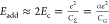 , where CΣ is the total capacitance of the QD and
  is the lever arm. From the height
and width
of the diamonds at large positive and negative voltage, we extract Eadd ∼ 12 meV and α = 0.2, which
yields D ∼ 60–70 nm. Our tight binding
simulations of irregularly shaped islands ∼60 nm in diameter
support the above assumptions, yielding an average Δ ∼
0.2–0.4 meV in the energy range [0,1] eV, see Figure S9.
is the lever arm. From the height
and width
of the diamonds at large positive and negative voltage, we extract Eadd ∼ 12 meV and α = 0.2, which
yields D ∼ 60–70 nm. Our tight binding
simulations of irregularly shaped islands ∼60 nm in diameter
support the above assumptions, yielding an average Δ ∼
0.2–0.4 meV in the energy range [0,1] eV, see Figure S9.
Figure 2.

(a) Conductance peaks measured over the whole gate range (±5 V) showing suppressed conductance around 0–2 V and sharp resonances in the electron and hole regimes. The vertical gray dotted line indicates the position of the CNP before breaking the junction. Stability diagrams of the current as a function of VSD (±25 mV) and VG measured at different gate regions: (b) at the hole regime, (c) at the charge neutrality point, and (d) at the electron regime.
We note that the Coulomb diamonds become irregular in shape and spacing near the CNP (Figure 2c). Such irregular dots around CNP have been observed in transport measurements of graphene constrictions19,20 and have been attributed to charge localization by the formation of charge puddles. The origin of the QD dominating at high/low gate voltages will be discussed below.
In Figure 3 we illustrate the effect of the bending height, Δz, (which is proportional to the relative in-plane displacement of the two graphene edges) on the transport properties of the junction. We compare the stability diagrams and the conductance peaks for four values of Δz. Starting from the most “open” position (Figure 3a, e), the first diamonds begin to appear, and the conductance peak amplitudes are relatively small (tenths of nanosiemens (nS)) with narrow line widths. The peaks can be fitted using the expression for the classical Coulomb blockade regime (Γ, Δ ≪ kBT ≪ 2Ec) where G ∝ cosh–2 (eαδVG/2.5kBTe), and δVG = VG – δVGpeak. This fit yields a Te of 4.2 K, close to the base temperature of our cryostat, which indicates that the peak broadening is limited by temperature rather than the lifetime of the resonance. These characteristics are evidence of weak coupling of the QD to the reservoirs. Upon closing the junction (Figure 3b, f) the sharp-edged diamonds fully close and extra lines parallel to the edges are seen inside the sequential tunnelling regions (i.e., excited states of the QD). Furthermore, the conductance peaks increase in amplitude and in width. Further closing of the gap (Figure 3c, g) causes the features in the stability diagram to start blurring, and correspondingly, the conductance peaks become broader, such that the tails of adjacent peaks overlap and the baseline conductance acquires a nonzero background. Finally, in Figure 3d and h, the features are almost completely smeared out, although the diamond shapes can still be discerned. The conductance peak amplitudes decrease while their width continues to increase. In this regime the peaks can be fitted with a Breit–Wigner resonance and are characterized by tails that have a slower decay than expected for a thermally broadened peak. This marks the onset of the strong electronic coupling regime.
Figure 3.

(a–d) Differential conductance as a function of bias and gate voltage during mechanical closing of the junction in the hole regime. (e–h) Corresponding conductance peaks measured with a lock-in preamplifier with an AC-bias amplitude of 100 μV.
In the following we investigate the influence of electrode displacement on the capacitive couplings of the QD. To this end, we select a gate range containing one full diamond in the hole regime and monitor it over a range of bending heights (Figure 4). It is evident that the diamond tilts during closing of the gap, indicating a continuous change in the symmetry of the capacitive couplings. Concurrently, the features become more smeared out, suggesting a change in the contact transparencies (tunnel couplings). The effect of mechanical displacement is reversible and the features are highly reproducible over several opening-closing cycles. This is demonstrated by monitoring the evolution of the Coulomb peaks over several opening–closing cycles over a wide displacement range, as shown in Figure S4.
Figure 4.

Differential conductance map of a selected Coulomb diamond for in-plane displacements (i.e., graphene overlap lengths) of (a) 0.8 nm, (b) 1 nm, (c) 1.3 nm, (d) 2.1 nm, (e) 2.7 nm, and (f) 3.4 nm.
Given the strong variation of the electrical properties with electrode displacement, in Figure 5 we analyze two properties of the system in more detail, i.e., (i) the capacitive coupling and (ii) the tunnel coupling of the QD to the source and drain electrodes.
Figure 5.

(a) Capacitances as a function of bending height (bottom x-axis) and in-plane displacement (i.e., overlap length, top x-axis) of the gate (yellow), source (magenta), and drain (blue), extracted from the slopes of the diamonds in Figure 4. (b) Mean height of the conductance peaks in the gate voltage window between −4.1 V and −3.5 V, as a function of displacement (circles). The solid line indicates the fit to the data using a Landauer approach at a fixed temperature 4.2 K, a calculated source tunnel coupling, ΓS, of 0.1 μeV, a graphene layer separation of 0.335 nm, and an overlap region width of 160 nm. (c) Drain tunnel coupling as a function of graphene overlap displacement. The inset shows the same coupling on a logarithmic scale. (d) Schematic illustration of the mechanical quantum dot model; the QD is located on the source-side of the graphene junction. The drain edge moves closer (further) to it during closing (opening), giving rise to the variation in the drain tunnel and capacitive couplings.
The capacitive couplings of a QD to the source (CS) and to the drain (CD) can
be extracted from the positive slope  and negative slope
  of the Coulomb diamond.21 In Figure 5a we plot CS and CD extracted from Coulomb diamonds recorded at
different bending
heights for the same displacement range used in Figure 4. The gate capacitance is estimated from
the addition energy assuming Eadd ≈
2Ec and using
of the Coulomb diamond.21 In Figure 5a we plot CS and CD extracted from Coulomb diamonds recorded at
different bending
heights for the same displacement range used in Figure 4. The gate capacitance is estimated from
the addition energy assuming Eadd ≈
2Ec and using  . Figure 5a shows that while CG and CS remain constant over the
displacement range,
with values of 3.1 aF and 3.5 aF, respectively, CD is initially (i.e., for larger electrode displacements)
lower than CS but continues to increase from ∼4 aF to ∼19
aF. This demonstrates that the capacitive coupling of the quantum
dot can be tuned by almost a factor of 5 by mechanical displacement
of the electrodes.
. Figure 5a shows that while CG and CS remain constant over the
displacement range,
with values of 3.1 aF and 3.5 aF, respectively, CD is initially (i.e., for larger electrode displacements)
lower than CS but continues to increase from ∼4 aF to ∼19
aF. This demonstrates that the capacitive coupling of the quantum
dot can be tuned by almost a factor of 5 by mechanical displacement
of the electrodes.
We now use this data to convert the bending
height into an in-plane
displacement of the graphene electrodes. To this end we assume that
the drain capacitor, which can be tuned mechanically, is formed from
the drain graphene electrode which partially overlaps with the graphene
quantum dot. The overlap area A = wd is given by the width of the constriction (w = 160 nm extracted by atomic force microscopy) and the
overlap d. By bending the sample, d = d0 – FΔz is changed, where F is the attenuation
factor of the junction (see SI Section S6). This changes the capacitance by 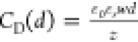 , where z = 0.335 nm is
the intersheet distance for graphene stacks and εr= 1. A fit to the data is shown in Figure 5a which yields the attenuation factor F that we use to convert the bending height into displacement d (see top x-axis in Figure 5A).
, where z = 0.335 nm is
the intersheet distance for graphene stacks and εr= 1. A fit to the data is shown in Figure 5a which yields the attenuation factor F that we use to convert the bending height into displacement d (see top x-axis in Figure 5A).
In the following we investigate the effect of displacement on the tunnel coupling between the quantum dot and the electrodes. In Figure 5b the average conductance ⟨G⟩ of the Coulomb peak maxima in a given gate voltage window (−4.1 V < VG < −3.9 V) is plotted over a wider in-plane displacement range of ∼6 nm. When increasing the displacement (moving contacts closer together), ⟨G⟩ increases to a maximum value of about 40 nS but decreases when d is increased further. Given that ⟨G⟩ is a measure of the strength and symmetry of the tunnel couplings to the source and drain leads, the data provide evidence that this symmetry is broken during the closing cycle.
The capacitive data discussed above clearly show that displacing the electrodes affects only one side of the junction. We therefore attribute the modulation of ⟨G⟩ with d to a change of the tunnel coupling ΓD between the QD and the drain electrode while we assume that the tunnel coupling ΓS between the QD and the source electrode stays constant. Similar observations of displacement-dependent capacitances and tunnel couplings have also been reported in other material systems, including single-molecule transistors consisting of a C60 molecule trapped between two gold electrodes in a mechanical break junction setup.22,23
A first estimate of ΓS can be made by modeling the dI/dV data in the regime of Figure 3h using a Landauer approach,24 where each peak can be fitted by
| 1 |
around the center E0 of the peak. Here, the transmission function T(E) is modeled by a Breit–Wigner resonance, where f(E) is the Fermi–Dirac distribution and  .
.
We thereby obtain ΓS ∼ 0.01–0.1 μeV. G(ΓD) reaches a maximum at ΓS = ΓD, where the height of the maximum is given by the total tunnel coupling ΓS + ΓD and the temperature T. To estimate the change in tunnel coupling ΓD(d) when varying the overlap area between the graphene quantum dot and the graphene drain electrode, we performed tight binding calculations of graphene QDs connected to or overlapped with the graphene electrodes (see SI Section S8). We find that ΓD displays oscillations as a function of d, possibly due to Fabry–Pérot interferences,17 whose envelope is given by ΓD(d) = 3d4 μeV within the distance range of the simulations, where d is measured in nanometers (Figure 5c). The behavior of ⟨G⟩ as a function of d shown in Figure 5b can be modeled equating the expression for the envelope to ΓD(d) in Eq 1, where the only free fitting parameter is ΓS. We find ΓS ≈ 0.1 μeV. Our tight binding transport simulations indicate that this small coupling is compatible with narrow source-dot connections having a width of the order of a few nanometers (see SI Section S9).
The capacitive and tunnel coupling data clearly show that displacing the electrodes affects only one side of the junction, as schematically shown in the circuit diagram of the junction (Figure 5d). The graphene QD is located between the graphene source and drain leads and is capacitively coupled to the graphite back gate (CG). During mechanical displacement (d) of the graphene leads, the tunnel barrier to the source remains approximately constant, leading to a fixed ΓS and CS. Conversely, ΓD and CD are modulated mechanically (blue arrow) and show a strong dependence on d, with ΓD changing from 10–4 eV for displacements of 6 nm to 10–9 eV at zero displacement, which corresponds to a sizable, 5 orders of magnitude, modulation of the tunnel barrier.
Discussion
The uniaxial straining of the monolayer graphene bowtie device has two effects on the electronic transport measurements. First, it can lead to reduction of out-of-plane height fluctuations (i.e., wrinkles, corrugations), which typically act as sources of disorder. Limiting this scattering mechanism has been shown to result in enhanced charge carrier mobility,16 which manifests itself in steeper slopes in the I–VG curves (Figure 1d, e). Second, smoothening out the wrinkles can also account for the formation of a small bilayer graphene overlap region upon closing of the gap,17 as the effective length of the graphene leads is increased.
The subsequent low-temperature transport measurements in the open nanogap regime indicate the presence of a stable, single graphene QD after mechanical breaking of the bowtie. The clean transport features are comparable to those of QDs formed via electrostatic gating in monolayer and bilayer graphene.10,25 While tearing of monolayer graphene nanoconstrictions is predicted to lead to atomically ordered edges,26 the edges of our device are likely passivated by edge groups during gap opening in air. Our data thus demonstrates that such edge terminations do not adversely impact transport across the gap. We further show that by changing the overlap area between the QD and drain electrode we achieve a high tunability of the tunnel and capacitive coupling, in the former case by over 5 orders of magnitude. The flexible control over the tunnel barrier strength and symmetry allows us to clearly observe the evolution from a strongly to a weakly coupled graphene QD system.
The formation of graphene QDs has been previously observed in lithographically defined graphene nanoconstrictions19 and in electroburned nanobowties27,28 and is typically attributed to charge localization at graphene edges. In short and narrow constrictions, the regions on which localization occurs can be several tens of nanometers long (i.e., significantly larger than the dimensions of the constrictions). We therefore performed tight binding transport simulations to identify possible realizations of a QD that can be compatible with a constant but extremely small ΓS coupling, constant capacitive couplings CS and CG, and varying CD and ΓD, as well as the ability to fill 80 electrons/holes that produce a regular set of Coulomb diamonds outside the transport gap. We find that these facts are consistent with the formation of a relatively large QD island (∼60 nm in diameter) in which electrons are geometrically confined, connected to the source electrode by a very narrow neck of width in the nanometer range, and that is overlapped by the drain electrode (see SI Sections S8 and S9).
Our data further indicate that additional QDs form inside the graphene constriction when the gate voltage reaches the CNP. It is unlikely that the additional dots are in parallel to the dominating QD, since these would provide alternative transport pathways and hence lead to nonzero current inside the Coulomb diamonds. Our simulations also exclude a random distribution of energy level characteristic of a chaotic QD as the source of the Coulomb diamond irregularities. We instead conclude that additional QDs are in series with the dominating QD. Given their strong size dependence on VG, these irregular, nonclosing Coulomb diamonds might originate from charge localization by charge puddles that form around the graphene leads or the graphene QD around the CNP.
Conclusion
In summary, the platform presented here combines the advantages of mechanically controlled two-terminal junctions and three-terminal devices with electrostatic control to probe the electronic transport through graphene nanoconstrictions. Our device design allows for unprecedented tunability of graphene QD transport features and is an alternative approach to the electrostatic control used to tune the coupling strength of QDs in bilayer graphene.10 In particular, this platform is attractive to study physical details, such as the effect of tunnel coupling asymmetry on device operation, that are crucial in applications such as quantum calorimetry and energy harvesting.14,15 We anticipate that this experimental platform will also be extended to other 2D materials with the prospect of exploring the low-temperature transport behavior under electrical and mechanical influence. In particular, it can lend itself to the formation, rupture, and controlled overlap of ultranarrow constriction in superconducting thin films, thereby providing a novel approach to manipulating the Josephson effect in an in-plane device.
Acknowledgments
S.C. acknowledges a Marie Skłodowska-Curie Individual Fellowship under grant BioGraphING (ID: 798851) and P.G. acknowledges a Marie Skłodowska-Curie Individual Fellowship under grant TherSpinMol (ID: 748642) from the European Union’s Horizon 2020 research and innovation programme. K.W. and T.T. acknowledge support from the Elemental Strategy Initiative conducted by the MEXT, Japan, and the CREST (JPMJCR15F3), JST. This work was supported by the Graphene Flagship (a European Union’s Horizon 2020 research and innovation programme under grant agreement no. 649953), the Marie Curie ITN MOLESCO, an ERC advanced grant (Mols@Mols no. 240299), and a Spanish MCIU/AEI/FEDER project (PGC2018-094783).
Supporting Information Available
The Supporting Information is available free of charge at https://pubs.acs.org/doi/10.1021/acs.nanolett.0c00984.
(S1) Methods; (S2) device yield; (S3) junctions before and after measurement; (S4) conductance during opening of a nanogap at 4 K; (S5) reversibility of transport features during cycling; (S6) calculation of the attenuation factor F; (S7) nature of the quantum dot; (S8) tight binding estimates of the tunnel couplings for different scenarios; (S9) tight binding estimates of the single-particle addition energies for dot islands (PDF)
Author Present Address
# S.C.: Department of Precision and Microsystems Engineering, Delft University of Technology, Mekelweg 2, 2628 CJ Delft, The Netherlands.
Author Present Address
∇ M.H.: Department of Physics, University of Basel, Klingelbergstrasse 82, CH-4056 Basel, Switzerland.
Author Present Address
○ P.G.: IMEC, Kapeldreef 75, B-3001 Leuven, Belgium.
Author Contributions
The manuscript was written through contributions of all authors. All authors have given approval to the final version of the manuscript.
The authors declare no competing financial interest.
Supplementary Material
References
- Trauzettel B.; Bulaev D. V.; Loss D.; Burkard G. Spin Qubits in Graphene Quantum Dots. Nat. Phys. 2007, 3, 192–196. 10.1038/nphys544. [DOI] [Google Scholar]
- He Y.; Gorman S. K.; Keith D.; Kranz L.; Keizer J. G.; Simmons M. Y. A Two-Qubit Gate between Phosphorus Donor Electrons in Silicon. Nature 2019, 571, 371–375. 10.1038/s41586-019-1381-2. [DOI] [PubMed] [Google Scholar]
- Huang W.; Yang C. H.; Chan K. W.; Hensen B.; Leon R. C. C.; Fogarty M. A.; Hwang J. C. C.; Hudson F. E.; Itoh K. M.; Morello A.; et al. Fidelity Benchmarks for Two-Qubit Gates in Silicon. Nature 2019, 569, 532–536. 10.1038/s41586-019-1197-0. [DOI] [PubMed] [Google Scholar]
- Herrmann O.; Gould C.; Molenkamp L. W. Coulomb-Blockade Peak Spacing Statistics of Graphene Quantum Dots on SiO2. J. Appl. Phys. 2016, 120, 164304. 10.1063/1.4965303. [DOI] [Google Scholar]
- Eich M.; Pisoni R.; Pally A.; Overweg H.; Kurzmann A.; Lee Y.; Rickhaus P.; Watanabe K.; Taniguchi T.; Ensslin K.; et al. Coupled Quantum Dots in Bilayer Graphene. Nano Lett. 2018, 18, 5042–5048. 10.1021/acs.nanolett.8b01859. [DOI] [PubMed] [Google Scholar]
- Eich M.; Pisoni R.; Overweg H.; Kurzmann A.; Lee Y.; Rickhaus P.; Ihn T.; Ensslin K.; Herman F.; Sigrist M.; Watanabe K.; Taniguchi T. Spin and Valley States in Gate-Defined Bilayer Graphene Quantum Dots. Phys. Rev. X 2018, 8, 031023. 10.1103/PhysRevX.8.031023. [DOI] [Google Scholar]
- Güttinger J.; Stampfer C.; Libisch F.; Frey T.; Burgdörfer J.; Ihn T.; Ensslin K. Electron-Hole Crossover in Graphene Quantum Dots. Phys. Rev. Lett. 2009, 103, 046810. 10.1103/PhysRevLett.103.046810. [DOI] [PubMed] [Google Scholar]
- Schnez S.; Molitor F.; Stampfer C.; Güttinger J.; Shorubalko I.; Ihn T.; Ensslin K. Observation of Excited States in a Graphene Quantum Dot. Appl. Phys. Lett. 2009, 94, 012107. 10.1063/1.3064128. [DOI] [Google Scholar]
- Gehring P.; Sowa J. K.; Cremers J.; Wu Q.; Sadeghi H.; Sheng Y.; Warner J. H.; Lambert C. J.; Briggs G. A. D.; Mol J. A. Distinguishing Lead and Molecule States in Graphene-Based Single-Electron Transistors. ACS Nano 2017, 11, 5325. 10.1021/acsnano.7b00570. [DOI] [PMC free article] [PubMed] [Google Scholar]
- Volk C.; Neumann C.; Kazarski S.; Fringes S.; Engels S.; Haupt F.; Müller A.; Stampfer C. Probing Relaxation Times in Graphene Quantum Dots. Nat. Commun. 2013, 4, 1753. 10.1038/ncomms2738. [DOI] [PMC free article] [PubMed] [Google Scholar]
- Dean C. R.; Young a F.; Meric I.; Lee C.; Wang L.; Sorgenfrei S.; Watanabe K.; Taniguchi T.; Kim P.; Shepard K. L.; et al. oron Nitride Substrates for High-Quality Graphene Electronics. Nat. Nanotechnol. 2010, 5, 722–726. 10.1038/nnano.2010.172. [DOI] [PubMed] [Google Scholar]
- Thierschmann H.; Sánchez R.; Sothmann B.; Arnold F.; Heyn C.; Hansen W.; Buhmann H.; Molenkamp L. W. Three-Terminal Energy Harvester with Coupled Quantum Dots. Nat. Nanotechnol. 2015, 10, 854–858. 10.1038/nnano.2015.176. [DOI] [PubMed] [Google Scholar]
- Brange F.; Samuelsson P.; Karimi B.; Pekola J. P. Nanoscale Quantum Calorimetry with Electronic Temperature Fluctuations. Phys. Rev. B: Condens. Matter Mater. Phys. 2018, 98, 205414. 10.1103/PhysRevB.98.205414. [DOI] [Google Scholar]
- Hartmann F.; Pfeffer P.; Höfling S.; Kamp M.; Worschech L. Voltage Fluctuation to Current Converter with Coulomb-Coupled Quantum Dots. Phys. Rev. Lett. 2015, 114, 146805. 10.1103/PhysRevLett.114.146805. [DOI] [PubMed] [Google Scholar]
- Jaliel G.; Puddy R. K.; Sánchez R.; Jordan A. N.; Sothmann B.; Farrer I.; Griffiths J. P.; Ritchie D. A.; Smith C. G. Experimental Realization of a Quantum Dot Energy Harvester. Phys. Rev. Lett. 2019, 123, 117701. 10.1103/PhysRevLett.123.117701. [DOI] [PubMed] [Google Scholar]
- Wang L.; Makk P.; Zihlmann S.; Baumgartner A.; Indolese D. I.; Watanabe K.; Schönenberger C.; Taniguchi T. Mobility Enhancement in Graphene by in Situ Reduction of Random Strain Fluctuations. Phys. Rev. Lett. 2020, 124, 157701. 10.1103/PhysRevLett.124.157701. [DOI] [PubMed] [Google Scholar]
- Caneva S.; Gehring P.; García-Suárez V. M.; García-Fuente A.; Stefani D.; Olavarria-Contreras I. J.; Ferrer J.; Dekker C.; van der Zant H. S. J. Mechanically Controlled Quantum Interference in Graphene Break Junctions. Nat. Nanotechnol. 2018, 13, 1126–1131. 10.1038/s41565-018-0258-0. [DOI] [PubMed] [Google Scholar]
- Young A. F.; Dean C. R.; Meric I.; Sorgenfrei S.; Ren H.; Watanabe K.; Taniguchi T.; Hone J.; Shepard K. L.; Kim P. Electronic Compressibility of Layer-Polarized Bilayer Graphene. Phys. Rev. B: Condens. Matter Mater. Phys. 2012, 85, 235458. 10.1103/PhysRevB.85.235458. [DOI] [Google Scholar]
- Bischoff D.; Libisch F.; Burgdörfer J.; Ihn T.; Ensslin K. Characterizing Wave Functions in Graphene Nanodevices: Electronic Transport through Ultrashort Graphene Constrictions on a Boron Nitride Substrate. Phys. Rev. B: Condens. Matter Mater. Phys. 2014, 90, 115405. 10.1103/PhysRevB.90.115405. [DOI] [Google Scholar]
- Todd K.; Chou H.; Amasha S.; Goldhaber-Gordon D. Quantum Dot Behavior in Graphene Nanoconstrictions. Nano Lett. 2009, 9, 416–421. 10.1021/nl803291b. [DOI] [PubMed] [Google Scholar]
- Hanson R.; Kouwenhoven L. P.; Petta J. R.; Tarucha S.; Vandersypen L. M. K. Spins in Few-Electron Quantum Dots. Rev. Mod. Phys. 2007, 79, 1217. 10.1103/RevModPhys.79.1217. [DOI] [Google Scholar]
- Champagne A. R.; Pasupathy A. N.; Ralph D. C. Mechanically Adjustable and Electrically Gated Single-Molecule Transistors. Nano Lett. 2005, 5, 305–308. 10.1021/nl0480619. [DOI] [PubMed] [Google Scholar]
- Grüter L.; Cheng F.; Heikkilä T. T.; González M. T.; Diederich F.; Schönenberger C.; Calame M. Resonant Tunnelling through a C60 Molecular Junction in a Liquid Environment. Nanotechnology 2005, 16, 2143–2148. 10.1088/0957-4484/16/10/029. [DOI] [PubMed] [Google Scholar]
- Gehring P.; Harzheim A.; Spièce J.; Sheng Y.; Rogers G.; Evangeli C.; Mishra A.; Robinson B. J.; Porfyrakis K.; Warner J. H.; et al. Field-Effect Control of Graphene-fullerene Thermoelectric Nanodevices. Nano Lett. 2017, 17, 7055–7061. 10.1021/acs.nanolett.7b03736. [DOI] [PubMed] [Google Scholar]
- Banszerus L.; Frohn B.; Epping A.; Neumaier D.; Watanabe K.; Taniguchi T.; Stampfer C. Gate-Definede Electron-Hole Double Dots in Bilayer Graphene. Nano Lett. 2018, 18, 4785–4790. 10.1021/acs.nanolett.8b01303. [DOI] [PubMed] [Google Scholar]
- Moura M. J. B.; Marder M. Tearing of Free-Standing Graphene. Phys. Rev. E 2013, 88, 032405. 10.1103/PhysRevE.88.032405. [DOI] [PubMed] [Google Scholar]
- Moser J.; Bachtold A. Fabrication of Large Addition Energy Quantum Dots in Graphene. Appl. Phys. Lett. 2009, 95, 173506. 10.1063/1.3243690. [DOI] [Google Scholar]
- Gehring P.; Sadeghi H.; Sangtarash S.; Lau C. S.; Liu J.; Ardavan A.; Warner J. H.; Lambert C. J.; Briggs G. A. D.; Mol J. A. Quantum Interference in Graphene Nanoconstrictions. Nano Lett. 2016, 16, 4210–4216. 10.1021/acs.nanolett.6b01104. [DOI] [PubMed] [Google Scholar]
Associated Data
This section collects any data citations, data availability statements, or supplementary materials included in this article.