

Abstract

It is well-known that grain boundaries (GBs) increase the electrical resistivity of metals due to their enhanced electron scattering. The resistivity values of GBs are determined by their atomic structure; therefore, assessing the local resistivity of GBs is highly significant for understanding structure–property relationships. So far, the local electrical characterization of an individual GB has not received much attention, mainly due to the limited accuracy of the applied techniques, which were not sensitive enough to detect the subtle differences in electrical resistivity values of highly symmetric GBs. Here, we introduce a detailed methodology to probe in situ or ex situ the local resistivity of individual GBs in Cu, a metallic model system we choose due to its low resistance. Both bulk Cu samples and thin films are investigated, and different approaches to obtain reliable and accurate resistivity measurements are described, involving the van der Pauw technique for macroscopic measurements as well as two different four-point-probe techniques for local in situ measurements performed inside a scanning electron microscope. The in situ contacts are realized with needles accurately positioned by piezodriven micromanipulators. Resistivity results obtained on coincidence site lattice GBs (incoherent Σ3 and asymmetric Σ5) are reported and discussed. In addition, the key experimental details as well as pitfalls in the measurement of individual GB resistivity are addressed.
Keywords: grain boundary, interface, electrical resistivity, thin films, copper
1. Introduction
Grain boundaries (GBs) are among the most significant defects influencing the electrical properties of metals.1−5 Specifically, many studies reveal that GBs are the dominant electron scattering source in metals, reporting a higher contribution to resistivity than surface scattering even for low dimensional materials such as thin films and nanowires.3−8 The acquisition of resistivity values for different GBs is a key parameter for the emerging studies involving the atomic structures, phases, and physical properties of GBs.9−13 However, only a few studies focus on the resistivity measurement of an individual GB and interconnect it with the atomic structure of the interface.13−17 Attempts to locally measure GB resistivity were limited by sample geometry, microstructure, and sensitivity of the corresponding electrical measurement techniques. Hence, additional experimental developments are required to locally sense the resistivity of individual GBs.
The atomic structure of a GB is determined by its crystallography, i.e., relative orientation between neighboring grains and the corresponding grain boundary plane, possible atomic translations at the GB, chemical composition, and temperature.10,12,18 Computational studies on particular GB types confirm that their structure determines the resistivity values.19−21 As a consequence, different types of coincidence site lattice (CSL) GBs can be distinguished by their values of resistivity. Moreover, theoretical and experimental studies show that segregation can either decrease or increase the GB resistivity depending on the GB type and alloying (impurity) element.17,19,22
The measurement of electrical resistivity of an individual GB in metals has been reported using several approaches. One possibility consists of measuring a macroscopic resistivity of a polycrystalline sample with a known number of GBs and then normalizing it by number of grains using mathematical models.1,5,23−25 A second approach considers growth of bulk bicrystals and then performing a measurement across a single GB.17 Various electrical measurement methods were employed for acquiring the electrical resistivity of GBs, e.g., Eddy currents,23 a potentiometer method,1 a superconducting quantum interface device (SQUID),17 and conducting atomic force microscopy.26 However, most of these methods can be exploited only at cryogenic temperatures. In the case of thin films, the most advanced technique for the direct measurement of GB resistivity is based on isolation of GBs from the surrounding materials by creating trenches around them and then performing local electrical measurements.4,14−16,27 The lines are either fabricated by focused ion beam (FIB) milling14,15 or by lithography fabrication processes employed in nano/microelectronics.4,6,16 On such structures, a single GB can be probed by an electrical measurement setup consisting of four needles. The needles, which are attached to piezostages enabling an accurate positioning, are designed for in situ scanning electron microscopy (SEM) operation and precise resistivity measurements. So far, only the resistivity of a high angle random GB containing tilt and twist components could be measured, while the resistivity of CSL and low angle GBs could not be resolved within the sensitivity limits of the measurement methods.14,15
Here, we introduce a detailed methodology enabling highly sensitive and accurate local resistivity measurement of individual GBs in bulk Cu and thin films. The paper presents crystal growth and sample preparation methods, details on the electrical measurement technique, as well as three different methods for local measurements of a single GB. Cu is used as a model material system, as it is heavily used in micro- and nanoelectronic devices as conduction lines. We measure the resistivity values of Σ3 and Σ5 GBs employing different techniques and compare the results. The presented methodology is highly relevant for the emerging studies on GB structures, segregation, phases, and resulting functional properties.
2. Experimental Section
2.1. Cu Bicrystal Growth and Cu Thin Film Deposition
In order to perform electrical measurements of an individual GB, careful crystal growth and sample preparation processes are required. Specifically, the samples must facilitate electrical measurements in a single crystal (i.e., selected region without GBs) and a bicrystal region (i.e., selected region separated by a single GB) within the same sample. Here, we briefly describe the Cu bicrystal growth process, Cu thin film deposition, and sample preparation method employed in this study.
Cu bulk bicrystals were grown by the conventional Bridgman method as described in detail in refs (9) and (28) using two seed crystals of preselected orientations. In the present case, two [100]-oriented seed crystals were used; one seed crystal was tilted by 36.9° along the [100] axis with respect to the other single crystal seed to form an asymmetric Σ5 tilt grain boundary in refs (9) and (28). To obtain a bulk bicrystal, a container of polycrystalline high purity Cu is in contact with the two seed crystals and heated slightly above the melting point. By slowly solidifying the melt zone, an asymmetric Σ5 [100] bicrystal forms. The bulk bicrystal is cut with spark erosion into 5 mm thick cylindrical slices with the Σ5 GB extending from the top to bottom surfaces of the slices. The atomic structure of the GB has been recently studied by advanced scanning transmission electron microscopy as reported in ref (9).
Cu thin films of high purity (99.999% pure Cu) were sputtered at room temperature on (0001)-oriented α-Al2O3 substrates (c-plane, 2″ sapphire wafers). Sputtering was carried out with a radio frequency (RF) power supply at 250 W, a background pressure of 0.66 Pa, and 20 sccm Ar flow. The deposition time to achieve a nominally 500 nm thick film was 45 min. Grain growth of the highly (111) textured Cu grains was achieved through post-thermal annealing at 400 °C for 3 h within the sputtering chamber in order to limit contamination and oxidation. The surface morphology and cross section were inspected with SEM (Zeiss-Gemini 500). Crystallographic orientation of thin film and GB planes are identified using electron backscattered diffraction (EBSD) SEM analysis (Zeiss Auriga SEM, EDAX EBSD detector, OIM software) at 12 kV. Subsequently, individual GBs can be selected based on the SEM-EBSD results and isolated within thin lines as described in Section 2.3.1.
2.2. Electrical Measurements
The contribution of an individual GB’s resistivity to the resistance of a pure metal is relatively low (∼2%).24 As a matter of fact, any current-induced heating, drift of a contact, or minor geometrical differences in samples might create deviation in measured resistance values within the same order of magnitude as that of the GB resistance. Therefore, the electrical measurement method must ensure that these factors are not affecting the experiment. For these reasons, persistent electrical measurements and an optimized modulation of electrical current are adapted for obtaining highly reliable data. The technique is based on applying a series of few hundreds of direct current (dc) pulses and measuring the corresponding voltage at each pulse. The same electrical measurement technique is used for all methods presented within this paper.
The electrical current is applied using a current generator (Keithly 6221) with 5–10 × 10–3 s long pulses. The deadtime between subsequent pulses is set to 20× the pulse time duration to avoid overlapping. A voltage measurement is conducted at the pulse half-time by employing a nanovoltmeter (Keithly 2182A). The height of the pulse varied between 0.05 and 50 mA, depending on the measurement geometry. Parameters of the pulses significantly affect the accuracy of measurements. For instance, Figure 1 presents the electrical resistance values and error bars obtained for a Cu single crystal through a four-point-probe technique with 60 μm spacing between needles. Resistance values are given for two pulse widths and four pulse heights. The data clearly show that increasing the pulse width from 5 to 10 ms yields a decrease of 50–60% in standard deviation values of resistivity. Moreover, an increase of pulse height from 5 to 50 mA shrinks the standard deviation by 11 times. Within such a geometry, utilizing 50 mA pulses of 10 ms width gives a standard deviation of 2%. The accuracy is further increased by repeating the experiment several times. In principle, higher currents yield a higher accuracy in resistance values, but high currents can induce Joule heating of the sample or contacts.
Figure 1.

Resistance values and error bars acquired by in situ four-point probe. Error bars decrease with increasing pulse width and height.
In case of applying only a single width dc pulse, an averaged voltage value over the duration of the pulse is obtained, and hence, any effects of heat or contact drift will be lost within the measurement time. However, repeated dc pulses of a certain duration reveal artifacts like heating and are the choice of technique to obtain reliable data. Figure 2 demonstrates the significance of utilizing the pulse technique; it shows resistance values obtained in Cu lines (detailed in Section 2.3.1) for three cases: reliable data, the joule heating effect, and the contact drift effect. If the electrical current is sufficiently high to cause heating of the sample, the increase in temperature with time is identified as a continuously monotonic increase in resistivity in the sequence of applied pulses (red points in Figure 2). In addition, in a case of a drift or weak mechanical contact of the needle while acquiring the measurement, the artifact will be detected as a nonuniform distribution of resistivity values along the sequence of the pulses even with sudden jumps in values (blue points in Figure 2). A reliable measurement is characterized by slightly and homogeneously scattered data points around a specific value for the consequent applied pulses, as described by the black points in Figure 2. To obtain reliable data, the dc pulse duration and deadtime must be carefully selected.
Figure 2.

Unwanted Joule heating and contact drift effects are recognized in the dc pulse technique by a monotonic increase (red) and nonstable (blue) values with consecutive pulses, respectively. Data of reliable measurements (black) are scattered around a single value.
In summary, the applied current for performing an experiment is chosen as the value that does not induce heating while yielding a high signal-to-noise ratio in the measured voltage. This typically requires some iterations in order to optimize the current, pulse duration, and deadtime. The sample is grounded while the measurement is performed for both ex situ and in situ experiments. In the latter case, Cu is short-cut with the stage of the SEM, while the electron beam is blanked during the resistivity measurements.
2.3. Resistivity Measurement Geometries
GB resistivity in a material is calculated by subtracting the resistivity of a single crystal from the resistivity of a bicrystal. Both the single crystal and bicrystal resistivity values are measured within the same sample to minimize errors from sample preparation conditions (e.g., unwanted impurities, surface roughness). In addition, using separate single crystal and bicrystal samples might induce systematic measurement errors due to variations in sample geometry. This statement is valid for all the techniques described in Section 2.3.
2.3.1. Thin Film Samples
In order to locally characterize an individual GB, the specific boundary must be electrically and physically isolated from any surrounding material. The geometry of measured features is chosen in a way that it enables calculation of resistivity ρ[μΩ·cm] from the measurement of the resistance R[Ω]. A convenient geometry is a line with length L and cross section A that contains i GBs; the resistance R of such a line is described by the analytical relation
| 1 |
where the term  in eq 1 captures the contribution of i GBs within
the line of cross section AGB. Each GB
possesses an individual resistivity γGB[Ω·cm2]. To simplify the analysis, the cross
section AGB of the individual GB should
be kept as identical as possible. Ideally, AGB = A. This means that for an inclined GB,
the area AGB > A,
and
it must be carefully determined. We discuss corrections and tolerance
in determining the AGB in Section 3. Also, effects like grain
boundary grooving require highly precise measurements to keep errors
in AGB at least 1 order of magnitude smaller
than the contribution of the GB to the measured resistance R compared to single crystal resistance.
in eq 1 captures the contribution of i GBs within
the line of cross section AGB. Each GB
possesses an individual resistivity γGB[Ω·cm2]. To simplify the analysis, the cross
section AGB of the individual GB should
be kept as identical as possible. Ideally, AGB = A. This means that for an inclined GB,
the area AGB > A,
and
it must be carefully determined. We discuss corrections and tolerance
in determining the AGB in Section 3. Also, effects like grain
boundary grooving require highly precise measurements to keep errors
in AGB at least 1 order of magnitude smaller
than the contribution of the GB to the measured resistance R compared to single crystal resistance.
In our study, a 400 °C annealing treatment for 3 h leads to sufficiently large grain sizes (>10 μm). Then, a line of typically more than 40 μm was cut in the thin film by milling trenches on a preselected area through the entire thickness of the film (Figure 3c). In our study, a Ga FIB was employed, and milling was done at a beam current of 50 pA. Figure 3 illustrates the described procedure. The ends of the line remain connected to the surrounding film in order to avoid charging effects by the insulating sapphire substrate during SEM imaging. Finally, local electrical properties are measured by probing the line using piezo-controlled needles accurately positioned inside the SEM (Figure 3d). During the resistivity measurements with the four probes, the electron beam of the SEM is blanked. Due to the absence of grooving and invisibility of GBs in secondary electron SEM imaging, the positions of GBs within the lines are determined by projecting the grain map of EBSD measurement after the FIB milling on the SEM image.
Figure 3.

(a) Thin films are grown on (0001)-oriented α-Al2O3 substrates; (b) grain growth is obtained by an annealing treatment. (c) GBs are separated from their surrounding region by FIB milling, and the line is still connected at its ends to the film. (d) Four micromanipulators are used to probe the bicrystal electrical resistivity.
The length of the lines is 40–60 μm, and the width is around 600 nm. The width is elected based on two considerations: (i) The width should exceed multiple times the mean free path of the electron in the inspected material to minimize effects from surface scattering; the mean free path of electrons in Cu at room temperature is 39 nm.29,30 (ii) The selected line width should support the mechanical contact load of the electrode tips placed on the line and keep drift of the electrode positions minimal.
Once the lines including the chosen GBs are prepared, the sample is inserted inside a SEM with four independent micromanipulators (Kleindiek Nanotechnik – PS4), each of them is equipped with a tungsten needle having a 50 nm curvature radius of the tip. The applied measurement geometry is illustrated in Figure 4; it consists of two needles (needles 1 and 2) with fixed positions at the edges of the line, which are used to apply a current. The other two needles are used for voltage measurement; one is fixed at a constant position within the line (needle 3), and the other is a mobile one moving in steps of ∼1 μm toward the other voltage contact (needle 3) from position 4 toward 4′′′ (see Figure 4). A series of resistivity measurements are conducted for different positions of needle 4. With this geometry, any measured resistivity value corresponds to the material within the volume between the voltage sensing needles 3 and 4 (Figure 4), including the resistivities of a known number of GBs. Thus, when the mobile needle 4 moves and crosses an individual GB, a jump in resistance R is observed—this value relates to the GB resistance.
Figure 4.

Schematic of a line containing several GBs within the thin film. Positions of the four needles used for the four-point measurement technique are demonstrated. Needles 1–3 are fixed at a specific position during the experiment, while needle 4 moves along the line from position 4 to 4′′′. Several GBs can be inspected within a single line.
2.3.2. Bulk Samples Using van der Pauw Method
The electrical resistivity measurement for bulk bicrystal has been carried out by adapting the van der Pauw method.31,32 This technique is applied in the present case on the cylindrical bicrystal containing the GB (see Figure 5a). For the resistivity measurement of the single crystal, all four needles must be positioned on one side of the bicrystal, i.e., in a single crystal region (see Figure 5a, positions 1 to 4). In that case, needle 4 is located in the vicinity of the GB (Figure 5a). In order to measure subsequently the resistivity of the bicrystal, needle 4 moves across the GB to position 4′, while needles 1 to 3 remain fixed at their previous position (Figure 5a). This approach eliminates systematic errors as three needles stay at the same position used for the single crystal resistivity measurement, while the fourth needle moves only a short distance across the GB in a location close to its initial position as illustrated in Figure 5a (see positions 4 and 4′). In order to confirm that the measured resistivity difference between the single and bicrystal corresponds to the presence of the GB rather than geometrical aspects, the resistivity measurements are conducted five times, repeatedly relocating the positions 4 and 4′ within the inspected region. Each measurement is obtained within a distance x from the edge of sample, where the GB intersects. Data presented in Figure 5b confirms the tolerance in positioning the needle. Changing the position of only one needle by ≤0.5 mm affects the measured values by ≤0.6%. This deviation is sufficiently small to measure an individual GB resistivity for Cu (see Figure 5b).
Figure 5.
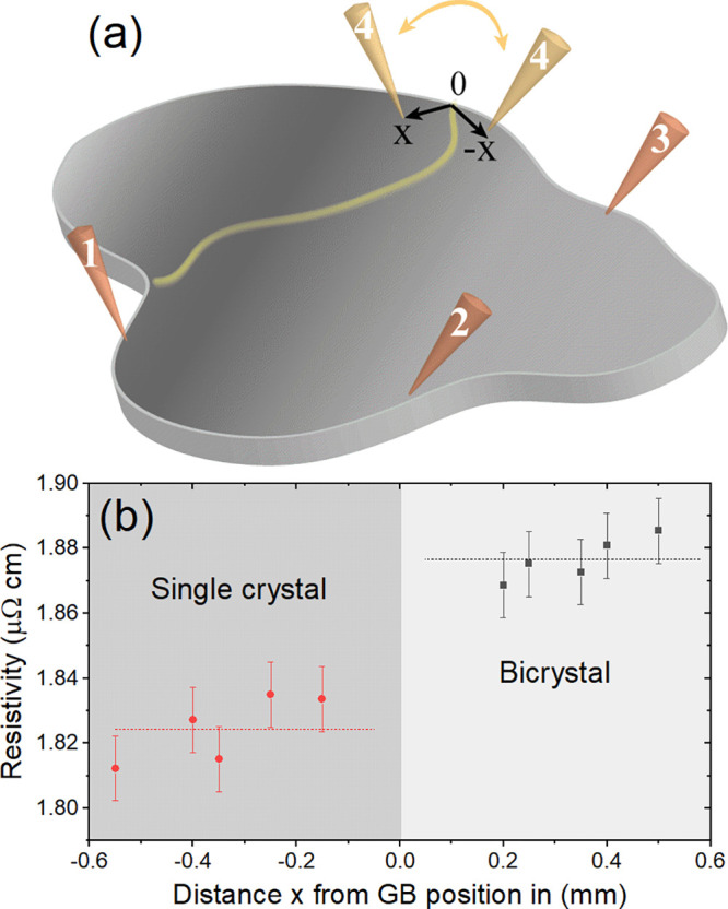
(a) Schematic of the van der Pauw method; needle positions 1 to 4 are applied for the resistivity measurements of a single grain of the bulk bicrystal, while positions 1 to 4′ sense the bicrystal resistivity. Note that needles 1–3 are kept in the same position during the experiment, while needle 4 is relocated to 4′. (b) Resistivities of the single and bicrystal obtained with sub-mm changes in needle positions 4 or 4′ near the GB.
The van der Pauw method consists of two resistivity measurements at fixed contact positions, while the two measurements are distinguished by altered connections of the contacts to the power supply and the voltmeter.31,32 We relate to each of the two measurements (connections) as a configuration. These are discussed in the Supporting Information. Choosing the right electrical connections at each of the configurations is highly important to obtain reliable values of GB resistivity. On that account, when performing the resistivity measurement on the bicrystal, the needle 4′ (Figure 5a), which is set across the GB, is always used for voltage output in both configurations. In that case, a current flows between the needles in the same crystal, and a voltage change is measured across the GB. Any other electrical connections in one of the van der Pauw configurations will result in asymmetric measurements across the GB—detailed analysis on contacting is provided in the Supporting Information and Figure S1.
2.3.3. Bulk Samples Using Four-Point-Probe Method
Another method for measuring GB resistivity in bulk bicrystal with arbitrary geometry or polycrystals with sufficiently large grains to host the contacts is the four-point-probe technique. The technique is applied using the bulk approximations,32 i.e., the spacing between needles is 5× less than thickness of the sample and the distance from edges as well as 25× less than sample diameter. In this study, the sample is inserted into a SEM chamber on a stage where four independent micromanipulators hold electrode needles that can be positioned in a linear configuration at specific locations. First, the needles are linearly and equidistantly arranged inside a single grain at a fixed distance, e.g., 20 μm, between each other. Then, the resistivity measurements are carried out (e.g., for positions 1–4, see Figure 6) and repeated for the other grain. Finally, to measure the resistivity of the bicrystal, the needles are arranged linearly at the same distances across the GB with needles 1′ and 2′ in grain A and needles 3′ and 4′ in grain B (see Figure 6). The subtraction of both values yields the contribution of a single GB to the resistivity. All measurements are repeated at least five times for statistical purposes.
Figure 6.

Schematic sketch illustrating the procedure to obtain GB resistivity by using the four-point-probe method. Single crystal resistivity is obtained for needles with positions 1 to 4; bicrystal resistivity can be deduced for needle positions 1′ to 4′.
Since each of the needles reaches the surface of the sample independently, a deviation in the spacing between them is expected. This deviation in position is caused either by a drift of the piezoelectric micromanipulators or by the user of the device due to misestimation of the exact position while landing the needles. The deviation in needle spacing is considered in the calculation of resistivity ρ by using eq 2(32)
| 2 |
where s1 and s3 are the spacings between the outer needles, while s2 is the distance between the middle needles. Hence, any deviation from intended distance is corrected with eq 2. Table 1 demonstrates the tolerance in the needle positions, which relates to measurements with a planned spacing of 20 μm between the needles. Table 1 reports the actual spacings, the corresponding resistance, as well as the calculated resistivity for three measurements for Cu. The resistivity values demonstrate that 5% tolerance in needle positions still provides an accuracy of 10–3 [μΩ·cm].
Table 1. Different Experiments to Measure Resistivity of Cu by In Situ Four-Point-Probe Technique.
| experiment | s1 [μm] | s2 [μm] | s3 [μm] | R [mΩ] | ρ [μΩ·cm] |
|---|---|---|---|---|---|
| 1 | 20.1 | 20.5 | 19 | 0.1427 | 1.710 |
| 2 | 19 | 20.2 | 20.6 | 0.1394 | 1.712 |
| 3 | 17.1 | 19.1 | 20.8 | 0.1460 | 1.703 |
It should be noted that in the case of Cu, no orientation dependent resistivity has been considered due to the isotropy of resistivity in face centered cubic crystals. However, if the material is anisotropic, the directions of electrical measurements (i.e., crystallographic direction along the linear needle array) must be considered before subtraction of the single and bicrystal resistivities, due to the directional dependence of electric properties.33
3. Analysis of Electrical Resistivity
3.1. GB Resistivity Measurement in Lines within Thin Films
The resistivity measurements of lines cut into thin films on insulating substrates are carried out by applying an analytical variation of a method present in the literature.4,14,15 First, having films with large grains enables resistivity measurements to be performed in long lines (tens of micrometers), and consequently, the resistance values are increased to magnitudes that are measurable with a high accuracy. This enables detection of slight changes in resistivity. Second, we consider imperfections in current measurement as described below. Our experimental approach deals with probing a single GB; thus, we present the calculation for this specific condition. If additional GBs are present in the line, they do not affect the calculation as long as they are eliminated when comparing the measurements of the two regions.
In an ideal case, a single GB is aligned perpendicular to the surface and parallel to the line cross section. In fact, {111} tilt GBs of annealed fcc metal films grown on sapphire substrates tend to have a columnar structure and align normal to surface, e.g., Cu and Al thin films.34,35 A tolerance in inclination of <3° keeps the error smaller than 10–3. If the GB plane is normal to the surface but its trace deviates by angle θ from the line’s cross section, eq 1 rewrites to
| 3 |
where V and I are measured voltage and applied current, respectively. However, the current supplied by the needles does not flow exclusively through the line but partially flows also within the thin film to which it remained connected at its ends. Hence, the measured resistance R̃ does not correspond to the applied current but to the part of current that flows in the line. Suppose that an unknown portion α < 1 of the applied current passes through the line; then, the actually measured resistance becomes
| 4 |
Considering an effective cross section defined as Aeff = α·A leads to
| 5 |
To obtain GB resistivity γGB, we follow these steps: First, the effective cross section is evaluated from the slope of the measured resistance as a function of distance between the voltage needles in a single crystal region—the first term in eq 5. The literature value ρ = 1.67 [μΩ·cm] is taken as the resistivity of pure Cu at room temperature.24,29,36,37 Second, we calculate the jump in resistance due to crossing the GB by subtracting the linearly fitted values measured for the single crystal from those obtained on the bicrystal. Finally, the jump in resistance yields γGB, since it equals the last term in eq 5. Note that the value of γGB is independent of α. Therefore, the variation in position of needles 1 and 2 will not affect the value of γGB. The angle θ is determined by SEM-EBSD imaging. The error in angle is 1°, corresponding to an error in order of 10–3 for θ < 3. The GB resistivity is calculated through the jump in the resistance values (see next section).
4. Results and Discussion
4.1. Electrical Resistivity of GBs in Thin Films
SEM-EBSD of the annealed Cu thin film reveals a sharp {111} texture (Figure 7a). All GBs are incoherent Σ3 boundaries with {211} type GB planes oriented along <110> directions as observed previously.38 A cross-sectional view of the thin film shows that GB planes are aligned perpendicular to the substrate. The maximal inclination of a GB along the film thickness is 2°. The uniform grain orientation of Cu thin films and the large grain size are well-known phenomena when depositing Cu on the basal plane of sapphire due to the sixfold symmetry of the substrate and threefold symmetry of the (111) plane of Cu.38,39 Grains expand laterally by a few micrometers and are thus large enough to locate four needles in different positions within the same grain. Cross-sectional imaging reveals a film thickness of 490 ± 10 nm, see Figure 7b. A line cut in the film containing several GBs is presented in Figure 7c; the in-plane directions are overlaid on the SEM image to reveal the positions of the GBs. Grooving remained too shallow be resolved in secondary electron SEM plan-view images. However, GBs became visible when tilting the sample and/or by SEM-EBSD studies.
Figure 7.

(a) Inverse pole figure [001] obtained by SEM-EBSD measurement on an annealed Cu thin film shows a {111} texture; the two twin-related grain orientation variants are distinguished by subtle contrast variations (GB marked by white lines). (b) Cross section SEM image reveals a GB aligned normal to surface; the arrow points toward the GB. (c) SEM image of a line within the thin film with the four needles for resistivity measurement. The SEM image is correlated with EBSD resolved in-plane directions to reveal the GBs.
Electrical measurements along the lines over the Σ3 {211} GBs show a linear relation between resistance and distance between voltage needles as predicted from eq 5. Figure 8b provides two examples of the linear relation probed at different Cu lines and GBs of the same type. It is obvious that the magnitudes of the measured resistance values of the two lines are different. This difference is attributed to the current, which flows outside the line in the connected film (parameter α), see Section 3. However, the different resistance values of the lines do not indicate a variation in the value of GB resistivity. On the contrary, subtraction of the linear fit of the resistance values of the corresponding part of the line without the GB of interest yields the same magnitude in resistance jump when crossing the GB (Figure 8c). Here, we demonstrate the accuracy of resistance measurements for the jump in resistance; for instance, the jump in resistance within the blue data in Figure 8 is 0.0118 ± 0.0018 Ω. By using eq 5, a direct measurement of the Σ3 {211} GB resistivity is accomplished. Averaging over seven measurements for different lines yields a value of 1.06·10–12 ± 0.1 Ω·cm2 for the Σ3 {211} GB.
Figure 8.

(a) Electrical measurements on an individual GB within a Cu line cut into the film. The position of the GB is defined as zero. The resistance values are measured between needles 3 and 4 for different positions of needle 4, with and without the Σ3 {211} Cu GB of interest. (b) Resistance follows a linear trend for varying positions of needle 4. Data acquired from two lines are provided as examples. (c) The GB resistivity causes a jump in resistance when subtracting the linearly extrapolated resistance of the single grain region of the line from the data containing the GB. The data from both Cu lines coincide in GB resistance for the incoherent Σ3 {211} Cu GB.
The measured value of Σ3 GB resistivity (1.06·10–12 ± 0.1 Ω·cm2 matches the order of magnitude of the average GB resistivity reported for Cu, which is in range of (0.15–4)·10–12 Ω·cm2.1,5,20,21,24 For a Cu coherent Σ3 GB, DFT calculations reported a resistivity of 0.2 × 10⁻¹² Ω·cm.20,21 Our measured value is higher than the calculated prediction due to several reasons:
The measurements are performed at room temperature, in which electron–phonon interaction is a major scattering mechanism, while this interaction is neglected in the calculation.
There is a difference in resistivity between coherent and incoherent Σ3 GBs due to a different atomic structure at the GB.
In addition, possible enrichment of Ga at the GB introduced by FIB milling may also affect the resistivity, although earlier studies indicate that Ga did not enrich at GBs in the lines within the reported resolution limit of 0.5 at. %.13 According to the phase diagram, Ga solubility in Cu exceeds 10 at. % at room temperature.40,41 But, usually, thermodynamic equilibrium is not achieved after FIB milling. Hence, some accumulation of Ga at GBs is still possible and might affect the measured GB resistivity14 but was too low to be resolved by SEM-EDS.
4.2. Electrical Resistivity of GBs in Bulk Cu
The bicrystal with the asymmetric Σ5 GB was measured on the common {100} surface using both approaches, the van der Pauw and the in situ four-point-probe technique. For the van der Pauw method, the four contacts are positioned as described in Section 2.3.2. Figure 9a shows a photograph of the bicrystal, the four contacts, and, as an artificially colored overlay, the information on the SEM-EBSD grain map revealing the GB position. The average resistivity value of the single crystal is subtracted from the average resistivity value of the bicrystal to obtain the contribution of the asymmetric Σ5 GB to the resistivity (see Table 2). This data corresponds to measurements presented in Figure 5b. The specific GB resistivity is not reported in this case, since the effective cross section of the GB is unknown. Alternatively, the GB resistivity is expressed as a contribution to the resistivity of the single crystalline material due to presence of the GB. Resistivity measurements of the same sample performed with the in situ four-point-probe method, where the needle positions are presented in Figure 9b, reveal similar values (Table 2).
Figure 9.
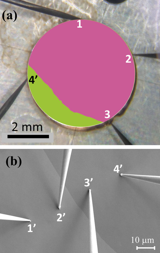
(a) van der Pauw contacts of the Cu bicrystal. The color code indicates the two grains based on SEM-EBSD measurement. (b) In situ four-point probe measurements across an individual GB in the bulk Cu.
Table 2. Contribution of an Individual Asymmetric Σ5 GB in Cu to the Resistivity of the Adjacent Single Crystal Measured by van der Pauw and Four-Point-Probe Techniquesa.
| GB resistivity
contribution to adjacent Cu single
crystal |
||
|---|---|---|
| GB type | absolute value (μΩ·cm) | relative value (%) |
| asym. Σ5 (van der Pauw) | 0.052 ± 0.007 | 3.07 ± 0.4 |
| asym. Σ5 (four-point probe) | 0.048 ± 0.007 | 2.84 ± 0.4 |
| twin GB – literature24 | 0.07 | 4.19 |
| high angle GB – literature24 | 0.14 | 8.38 |
Differences between bicrystal and single crystal resistivities are presented. The average values reported in the literature are presented for comparison.
The measured contribution of the asymmetric Σ5 GBs to the adjacent Cu single crystals are compared to general Cu GBs reported in literature24 due to a lack of data on Σ5 Cu GBs. Note that the measured resistivity values in our study are lower than those reported in ref (24), which may be due to subtle differences in Cu purity and/or the periodicity of the GB structure. The latter could explain the higher relative change.
5. Conclusions
In this work, we provide protocols for direct local electrical resistivity measurements of individual GBs in thin metallic films and bulk metals using Cu as a case study. The results demonstrate the capability to directly measure the resistivity of a single CSL GB in a highly conductive material by combining precise electrical measurements, different contacting techniques, and suitable sample structures. The samples require currently grain sizes of >6 μm to enable precise positioning of the contacts. Electrical measurements are carried out using dc pulses to avoid noise caused by Joule heating and contact drift. The resistivity of an asymmetric Σ5 Cu GB is measured in a bulk Cu sample using the van der Pauw method as well as the local in situ four-point-probe technique. Resistivity values obtained by both techniques are in agreement. In addition, we were able to resolve the resistivity of a single incoherent Σ3 Cu GB in a thin film. The latter measurement is performed on lines within the film produced by FIB milling. The methodology described in this paper will enable systematic studies on relationships between GB resistivity and their structure in metals.
Acknowledgments
H.B. acknowledges the financial support by the ERC Advanced Grant GB CORRELATE (Grant Agreement 787446 GB-CORRELATE) of G.D.
Supporting Information Available
The Supporting Information is available free of charge at https://pubs.acs.org/doi/10.1021/acsaelm.0c00311.
van der Pauw method applied for a single grain boundary (PDF)
Author Present Address
‡ Laboratoire des Sciences des Procédés et des Matériaux (LSPM), CNRS, Université Sorbonne Paris Nord, 93430 Villetaneuse, France. (M.G.)
The authors declare no competing financial interest.
Supplementary Material
References
- Andrews P. V.; West M. B.; Robeson C. R. The effect of grain boundaries on the electrical resistivity of polycrystalline copper and aluminium. Philos. Mag. 1969, 19 (161), 887–898. 10.1080/14786436908225855. [DOI] [Google Scholar]
- Mayadas A. F.; Shatzkes M. Electrical-Resistivity Model for Polycrystalline Films: the Case of Arbitrary Reflection at External Surfaces. Phys. Rev. B 1970, 1 (4), 1382–1389. 10.1103/PhysRevB.1.1382. [DOI] [Google Scholar]
- Wu W.; Brongersma S. H.; Van Hove M.; Maex K. Influence of surface and grain-boundary scattering on the resistivity of copper in reduced dimensions. Appl. Phys. Lett. 2004, 84 (15), 2838–2840. 10.1063/1.1703844. [DOI] [Google Scholar]
- Steinhögl W.; Schindler G.; Steinlesberger G.; Traving M.; Engelhardt M. Comprehensive study of the resistivity of copper wires with lateral dimensions of 100 nm and smaller. J. Appl. Phys. 2005, 97 (2), 023706. 10.1063/1.1834982. [DOI] [Google Scholar]
- Mannan K. M.; Karim K. R. Grain boundary contribution to the electrical conductivity of polycrystalline Cu films. J. Phys. F: Met. Phys. 1975, 5 (9), 1687–1693. 10.1088/0305-4608/5/9/009. [DOI] [Google Scholar]
- Pyzyna A.; Bruce R.; Lofaro M.; Tsai H.; Witt C.; Gignac L.; Brink M.; Guillorn M.; Fritz G.; Miyazoe H.; Klaus D.; Joseph E.; Rodbell K. P.; Lavoie C.; Park D. Resistivity of copper interconnects beyond the 7 nm node. 2015 Symposium on VLSI Technology 2015, T120. 10.1109/VLSIT.2015.7223712. [DOI] [Google Scholar]
- Cemin F.; Lundin D.; Cammilleri D.; Maroutian T.; Lecoeur P.; Minea T. Low electrical resistivity in thin and ultrathin copper layers grown by high power impulse magnetron sputtering. J. Vac. Sci. Technol., A 2016, 34 (5), 051506. 10.1116/1.4959555. [DOI] [Google Scholar]
- Munoz R. C.; Arenas C. Size effects and charge transport in metals: Quantum theory of the resistivity of nanometric metallic structures arising from electron scattering by grain boundaries and by rough surfaces. Appl. Phys. Rev. 2017, 4, 011102. 10.1063/1.4974032. [DOI] [Google Scholar]
- Peter N. J.; Frolov T.; Duarte M. J.; Hadian R.; Ophus C.; Kirchlechner C.; Liebscher C. H.; Dehm G. Segregation-Induced Nanofaceting Transition at an Asymmetric Tilt Grain Boundary in Copper. Phys. Rev. Lett. 2018, 121 (25), 255502. 10.1103/PhysRevLett.121.255502. [DOI] [PubMed] [Google Scholar]
- Liebscher C. H.; Stoffers A.; Alam M.; Lymperakis L.; Cojocaru-Miredin O.; Gault B.; Neugebauer J.; Dehm G.; Scheu C.; Raabe D. Strain-Induced Asymmetric Line Segregation at Faceted Si Grain Boundaries. Phys. Rev. Lett. 2018, 121 (1), 015702. 10.1103/PhysRevLett.121.015702. [DOI] [PubMed] [Google Scholar]
- Zhu Q.; Samanta A.; Li B.; Rudd R. E.; Frolov T. Predicting phase behavior of grain boundaries with evolutionary search and machine learning. Nat. Commun. 2018, 9 (1), 467. 10.1038/s41467-018-02937-2. [DOI] [PMC free article] [PubMed] [Google Scholar]
- Frolov T.; Setyawan W.; Kurtz R. J.; Marian J.; Oganov A. R.; Rudd R. E.; Zhu Q. Grain boundary phases in bcc metals. Nanoscale 2018, 10 (17), 8253–8268. 10.1039/C8NR00271A. [DOI] [PubMed] [Google Scholar]
- Malyar N. V.; Grabowski B.; Dehm G.; Kirchlechner C. Dislocation slip transmission through a coherent Σ3{111} copper twin boundary: Strain rate sensitivity, activation volume and strength distribution function. Acta Mater. 2018, 161, 412–419. 10.1016/j.actamat.2018.09.045. [DOI] [Google Scholar]
- Kim T.-H.; Nicholson D. M.; Zhang X.-G.; Evans B. M.; Kulkarni N. S.; Kenik E. A.; Meyer H. M.; Radhakrishnan B.; Li A.-P. Structural Dependence of Grain Boundary Resistivity in Copper Nanowires. Jpn. J. Appl. Phys. 2011, 50 (8), 08LB09. 10.7567/JJAP.50.08LB09. [DOI] [Google Scholar]
- Kim T.-H.; Zhang X.-G.; Nicholson D. M.; Evans B. M.; Kulkarni N. S.; Radhakrishnan B.; Kenik E. A.; Li A.-P. Large Discrete Resistance Jump at Grain Boundary in Copper Nanowire. Nano Lett. 2010, 10 (8), 3096–3100. 10.1021/nl101734h. [DOI] [PubMed] [Google Scholar]
- Kitaoka Y.; Tono T.; Yoshimoto S.; Hirahara T.; Hasegawa S.; Ohba T. Direct detection of grain boundary scattering in damascene Cu wires by nanoscale four-point probe resistance measurements. Appl. Phys. Lett. 2009, 95 (5), 052110. 10.1063/1.3202418. [DOI] [Google Scholar]
- Nakamichi I. Electrical Resistivity and Grain Boundaries in Metals. Mater. Sci. Forum 1996, 207–209, 47–58. 10.4028/www.scientific.net/MSF.207-209.47. [DOI] [Google Scholar]
- Brandon D. G. The structure of high-angle grain boundaries. Acta Metall. 1966, 14 (11), 1479–1484. 10.1016/0001-6160(66)90168-4. [DOI] [Google Scholar]
- Cesar M.; Gall D.; Guo H. Reducing Grain-Boundary Resistivity of Copper Nanowires by Doping. Phys. Rev. Appl. 2016, 5 (5), 054018. 10.1103/PhysRevApplied.5.054018. [DOI] [Google Scholar]
- Cesar M.; Liu D.; Gall D.; Guo H. Calculated Resistances of Single Grain Boundaries in Copper. Phys. Rev. Appl. 2014, 2 (4), 044007. 10.1103/PhysRevApplied.2.044007. [DOI] [Google Scholar]
- Valencia D.; Wilson E.; Jiang Z.; Valencia-Zapata G. A.; Wang K.-C.; Klimeck G.; Povolotskyi M. Grain-Boundary Resistance in Copper Interconnects: From an Atomistic Model to a Neural Network. Phys. Rev. Appl. 2018, 9, 044005. 10.1103/PhysRevApplied.9.044005. [DOI] [Google Scholar]
- Kim G.; Chai X.; Yu L.; Cheng X.; Gianola D. S. Daniel, Interplay between grain boundary segregation and electrical resistivity in dilute nanocrystalline Cu alloys. Scr. Mater. 2016, 123, 113–117. 10.1016/j.scriptamat.2016.06.008. [DOI] [Google Scholar]
- Kasen M. B. Grain boundary resistivity of aluminium. Philos. Mag. 1970, 21 (171), 599–610. 10.1080/14786437008238442. [DOI] [Google Scholar]
- Lu L.; Shen Y.; Chen X.; Qian L.; Lu K. Ultrahigh Strength and High Electrical Conductivity in Copper. Science 2004, 304 (5669), 422–426. 10.1126/science.1092905. [DOI] [PubMed] [Google Scholar]
- Bakonyi I.; Isnaini V. A.; Kolonits T.; Czigány Zs.; Gubicza J.; Varga L. K.; TóthKádár E.; Pogány L.; Péter L.; Ebert H. The specific grain-boundary electrical resistivity of Ni. Philos. Mag. 2019, 99 (9), 1139–1162. 10.1080/14786435.2019.1580399. [DOI] [Google Scholar]
- Bietsch A.; Michel B. Size and grain-boundary effects of a gold nanowire measured by conducting atomic force microscopy. Appl. Phys. Lett. 2002, 80 (18), 3346–3348. 10.1063/1.1473868. [DOI] [Google Scholar]
- Plombon J. J.; Andideh E.; Dubin V. M.; Maiz J. Influence of phonon, geometry, impurity, and grain size on Copper line resistivity. Appl. Phys. Lett. 2006, 89 (11), 113124. 10.1063/1.2355435. [DOI] [Google Scholar]
- Malyar N. V.; Springer H.; Wichert J.; Dehm G.; Kirchlechner C. Synthesis and mechanical testing of grain boundaries at the micro and sub-micro scale. Materialpruefung 2019, 61 (1), 5–18. 10.3139/120.111286. [DOI] [Google Scholar]
- Gall D. Electron mean free path in elemental metals. J. Appl. Phys. 2016, 119, 085101. 10.1063/1.4942216. [DOI] [Google Scholar]
- Gall D. The search for the most conductive metal for narrow interconnect lines. J. Appl. Phys. 2020, 127, 050901. 10.1063/1.5133671. [DOI] [Google Scholar]
- van der Pauw L. J. A method for measuring specific resistivity and hall effect of discs of arbitrary shapes. Philips Res. Repts 1958, 13, 1–9. [Google Scholar]
- Miccoli I.; Edler F.; Pfnür H.; Tegenkamp C. The 100th anniversary of the four-point probe technique: the role of probe geometries in isotropic and anisotropic systems. J. Phys.: Condens. Matter 2015, 27 (22), 223201. 10.1088/0953-8984/27/22/223201. [DOI] [PubMed] [Google Scholar]
- Martin N.; Sauget J.; Nyberg T. Anisotropic electrical resistivity during annealing of oriented columnar titanium films. Mater. Lett. 2013, 105, 20–23. 10.1016/j.matlet.2013.04.058. [DOI] [Google Scholar]
- Meiners T.; Duarte J. M.; Richter G.; Dehm G.; Liebscher C. H. Tantalum and Zirconium induced structural transitions at complex [111] tilt grain boundaries in Copper. Acta Mater. 2020, 190, 93–104. 10.1016/j.actamat.2020.02.064. [DOI] [Google Scholar]
- Hieke S. W.; Breitbach B.; Dehm G.; Scheu C. Microstructural evolution and solid state dewetting of epitaxial Al thin films on sapphire (ε-Al2O3). Acta Mater. 2017, 133, 356–366. 10.1016/j.actamat.2017.05.026. [DOI] [Google Scholar]
- Cho Y. C.; Lee S.; Ajmal M.; Kim W.-K.; Cho C. R.; Jeong S.-Y.; Park J. H.; Park S. E.; Park S.; Pak H.-K.; Kim H. C. Copper Better than Silver: Electrical Resistivity of the Grain-Free Single-Crystal Copper Wire. Cryst. Growth Des. 2010, 10 (6), 2780–2784. 10.1021/cg1003808. [DOI] [Google Scholar]
- Brandes E. A.; Brook G. B.. Smithells Metals Reference Book, 7th ed.; Butterworth-Heinemann: Oxford, U.K., 1998. [Google Scholar]
- Dehm G.; Rühle M.; Ding G.; Raj R. Growth and structure of copper thin films deposited on (0001) sapphire by molecular beam epitaxy. Philos. Mag. B 1995, 71 (6), 1111–1124. 10.1080/01418639508241899. [DOI] [Google Scholar]
- Dehm G.; Edongué H.; Wagner T.; Oh S. H.; Arzt E. Obtaining different orientation relationships for Cu films grown on (0001) α-Al 2 O 3 substrates by magnetron sputtering. Z. Metallkd. 2005, 96, 249–254. 10.3139/146.101027. [DOI] [Google Scholar]
- Jendrzejczyk-Handzlik D.; Fitzner K.; Gierlotka K. On the Cu–Ga system: Electromotive force measurement and thermodynamic reoptimization. J. Alloys Compd. 2015, 621, 287–294. 10.1016/j.jallcom.2014.08.037. [DOI] [Google Scholar]
- Muzzillo C. P.; Campbell C. E.; Anderson T. J. Cu–Ga–In thermodynamics: experimental study, modeling, and implications for photovoltaics. J. Mater. Sci. 2016, 51 (7), 3362–3379. 10.1007/s10853-015-9651-3. [DOI] [Google Scholar]
Associated Data
This section collects any data citations, data availability statements, or supplementary materials included in this article.