

Abstract
Tip-enhanced Raman scattering (TERS) in ångström-scale plasmonic cavities has drawn increasing attention. However, Raman scattering at vanishing cavity distances remains unexplored. Here, we show the evolution of TERS in transition from the tunneling regime to atomic point contact (APC). A stable APC is reversibly formed in the junction between an Ag tip and ultrathin ZnO or NaCl films on the Ag(111) surface at 10 K. An abrupt increase of the TERS intensity occurs upon APC formation for ZnO, but not for NaCl. This remarkable observation is rationalized by a difference in hybridization between the Ag tip and these films, which determines the contribution of charge transfer enhancement in the fused plasmonic junction. The strong hybridization between the Ag tip and ZnO is corroborated by the appearance of a new vibrational mode upon APC formation, whereas it is not observed for the chemically inert NaCl.
Keywords: Tip-enhanced Raman spectroscopy, Scanning tunneling microscopy, Plamonic picocavity, Atomic point contact, Ultrathin films
TERS has become a powerful tool for ultrasensitive chemical analysis in nanoscale environments.1 The ultrahigh sensitivity down to the single-molecule level relies on plasmonically enhanced Raman scattering in metallic nanocavities, so-called “hot spots”. Recently, it has been demonstrated that the exceptional high sensitivity can be obtained in subnanometer plasmonic cavities (picocavities), where sharply confined electromagnetic fields generated by atomic-scale asperities play a crucial role.2 First-principle simulations have also suggested that the field confinement reaches even atomic scales,3,4 which is supported by observing characteristic cavity modes of a well-controlled plasmonic dimer in white-light scattering5 and, more recently, by remarkable ångström-resolution Raman imaging in TERS at extremely small gap distances (<3 Å).6,7 Therefore, elucidating the nature of plasmonic fields and light–matter interactions in atomic-scale cavities is now of key importance for both fundamental physics and practical applications.
As the cavity size approaches the ångström scale, the plasmon mode undergoes a transition from the capacitively to the conductively coupled regime.8 The plasmonic field and enhanced Raman scattering in the capacitively coupled regime can be well described by classical electromagnetics and standard Raman scattering theories. On the other hand, Raman scattering in the conductively coupled regime is governed by charge transfer plasmons and direct scattering with optically induced currents,9 where a full quantum-mechanical and nonequilibrium treatment becomes necessary. In addition, it was reported that qualitatively different enhanced Raman spectra are observed when a molecule is electrically fused in a plasmonic junction.10,11 Although these measurements suggest a critical impact of a chemical interaction in conductively coupled junctions, the precise control of the gap distance is lacking and the evolution of Raman scattering at vanishing distances remains elusive.
In this Letter, we reveal the evolution of TERS intensities and spectra in an atomic-scale plasmonic cavity including transition from a tunneling regime to atomic point contact (APC) formation. Using the precise control of the gap distance in low-temperature scanning tunneling microscopy (STM), a stable APC is formed in a reproducible manner at 10 K between an Ag tip and a 2-monolayer (ML) thick ZnO or NaCl film grown on an Ag(111) surface. The measurements of these samples with a largely different electronic structure clarify that hybridization between the sample and the Ag tip has a critical impact on the TERS enhancement upon APC formation through the charge transfer mechanism, whereby an abrupt increase of TERS occurs in the ZnO film, whereas it is absent for the chemically inert NaCl films.
Figure 1a displays an STM image of ultrathin ZnO films epitaxially grown on the Ag(111) surface (see the Supporting Information for experimetal details). The hexagonal protrusions represent the Moiré pattern resulting from the lattice mismatch between the ZnO film and the surface.12,13Figure 1b illustrates the experiment, where TERS is recorded as a function of the relative displacement of the tip–sample distance (Δz) under continuous-wave laser excitation with wavelength λext. We used an electrochemically etched Ag tip further sharpened by focused ion beam (FIB) milling (Figure 1c and 1d), which enables control of localized surface plasmons in the STM junction.14Figure 1e shows the TER spectra measured for 2-ML ZnO at different Δz with λext = 633 nm, which leads to tip-enhanced resonance Raman scattering where both electromagnetic (EM) and chemical enhancement (via electronic resonance) are operative simultaneously.15 During the measurement the bias voltage (Vbias) is nominally set to zero, but there is an effective potential difference of ∼1 mV due to an instrumental offset and a photovoltage, resulting in measurable currents in the junction. Figure 1f shows the tunneling current (It) versus Δz. It increases exponentially in the tunneling regime until it exhibits a jump-to-contact behavior,16 i.e., APC formation, which defines Δz = 0 Å. The conductance at Δz = 0 Å is estimated to be ∼0.1 G0 (= e2/h = 77.6 μS) by measuring the It–Vbias curve. In the tunneling regime (Δz > 0 Å), the TERS intensity monotonically increases due to an increase of the plasmonic field in the junction. The intense peaks at 300–380 cm–1 can be assigned to the out-of-plane phonon modes of the ZnO film, whereas weak peaks at 200–300 and 500–600 cm–1 are assigned to the in-plane modes.15 The surface selection rule for metals17 leads to much larger enhancement for the out-of-plane modes than the in-plane modes.
Figure 1.

Gap-distance-dependent TERS measurement for 2-ML ZnO. (a) Quasi 3D STM image of ultrathin ZnO layers epitaxially grown on the Ag(111) surface (Vbias = 1 V, It = 100 pA). (b) Schematic of the measurement configuration. (c–d) Scanning electron micrograph of the FIB Ag tip. (e) TER spectra of 2-ML ZnO recorded at different Δz as indicated in the figure (Ag tip, λext = 633 nm, F = 0.29 mW μm–2, exposure time (texp) = 3 s per spectrum, 10 K). (f) It versus Δz acquired over 2-ML ZnO. The shaded area indicates the contact regime. Vbias is set to 0 V nominally, but there is an offset bias of ∼1 mV during the measurement. Δz = 0 corresponds to the distance at which point-to-contact occurs (formation of APC). The colored circles represent the point of the TER spectra in (e). The upper-right inset shows the magnified It–Δz curve around the APC. (g–h) TER spectra in the tunneling and contact regime, respectively. The red arrow in (h) indicates the “contact mode”.
In the vicinity of the APC, several remarkable changes are observed (Figures 1g and 1h). First, just before APC formation (Δz = 0.1 Å), the relative intensity of the in-plane modes is significantly increased. Second, the overall TERS intensity suddenly increases at the APC. Third, a new characteristic peak at ∼400 cm–1 appears in the APC regime (denoted as “contact mode”). Forth, a continuous background suddenly appears upon APC formation. We found that the background intensity is correlated with the TERS intensity and it may be related to the plasmonic field in the junction (Figure S1). The Raman intensity shows a linear power dependence in both tunneling15 and APC regime (Figure S2).
We demonstrate that the APC can be formed and broken in a reversible manner. Figure 2a displays a waterfall plot of the TER spectra during sequential approach and retraction of the Ag tip to and from 2-ML ZnO including both tunneling and APC regimes. The spectral evolution is symmetric with respect to the turning point (Δz = −1.3 Å), and thus, the process is nondestructive (reversible). It is clear that the contact mode appears immediately at the APC and blue-shifts linearly (16.6 ± 1.0 cm–1/Å) as Δz is further reduced (the tip is “squeezed” to the ZnO film), indicating a variation in the bond strength. The TERS intensity decreases as the Δz is further reduced in the APC regime (Δz < 0 Å), which may result from the attenuation of the plasmonic field because the continuous background also decreases. We examined different Ag tips, and these observations were highly reproducible (Figure S3).
Figure 2.
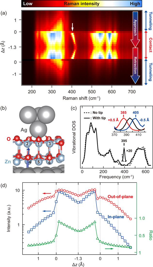
Evolution of TERS from tunneling to APC regime. (a) Waterfall plot of the gap-distance-dependent TER spectra recorded over 2-ML ZnO (Ag tip, λext = 633 nm, F = 0.36 mW μm–2, texp = 300 s per spectrum, 10 K). The tip approaches and retracts toward and backward from the ZnO from the tunneling to the APC regime. (b) Optimized structure with the Ag tip. The characteristic vibrational mode resulting from the quantum point contact is shown by the blue arrow. (c) Calculated vibrational density of states (VDOS) with and without the Ag tip. The inset shows the corresponding VDOS as a function of tip displacement. (d) Integrated Raman intensity of the out-of-plane (292–383 cm–1) and in-plane (489–644 cm–1) modes as a function of Δz (left axis). The continuous background in the TERS spectra is subtracted before integration. The ratio between these modes is also plotted (right axis).
Our density functional theory (DFT) calculations (see the Supporting Information for details) reveal that the contact mode can be assigned to the local out-of-plane stretching mode of the O atom in the second layer (Figure 2b). When the APC is formed, the Ag tip interacts with the O atoms in the first layer. The resulting charge rearrangement in the fused junction (Figure S5) causes elongation of the in-plane Zn–O bonds in both first and second layers underneath the tip, whereas the interlayer Zn–O bond shrinks (the average bond length changes by ∼0.26 Å). As a consequence, the interlayer bond between Zn atom #2 and O atom #4 becomes stiffer, which leads to a new vibrational mode at 395 cm–1 (Figure 2c). In order to examine a “pushing” effect by the tip in the contact regime, we calculated the vibrational frequency of the new mode at different tip–surface distances and found that, indeed, the Zn–O stretching mode blue-shifts at 20 cm–1/Å as the distance decreases because the bond gets stiffer (inset to Figure 2c). This is in excellent agreement with the experimental observation (Figure 2a), corroborating our assignment of the contact mode.
The relative intensity between the in- and out-of-plane phonon modes of 2-ML ZnO can be used to quantify the plasmonic field distribution as a function of Δz. The TERS intensities of these modes are primarily associated with the local field components perpendicular and parallel to the surface. The intensity of both modes exponentially varies in the tunneling regime (Figure 2d), and a moderate variation of their intensity ratio indicates the gradually increasing contribution of the in-plane field component and/or the field gradient of the tightly confined plasmon at the tip apex.18,19 The evolution of the plasmonic field in the STM junction is examined by electrodynamics simulations (Figure S6), which qualitatively reproduce a more rapid increase of the in-plane component, in good agreement with the experiment. On the other hand, when the APC is formed, the intensity of both in-plane and out-of-plane modes exhibit a discrete change and the relative intensity of the in-plane modes is largely increased. This should be associated with a sudden change of the polarizability of the ZnO film as discussed later. However, the plasmonic field distribution may not be affected upon APC formation because the overall spectral shape in TERS is essentially the same just before and after the contact except for the appearance of the contact mode (see the spectra at Δz = 0.1 and −0.3 Å in Figure 1c). If the field distribution is significantly modified, selection rules for Raman scattering should be changed, and consequently, the TERS spectra would exhibit qualitative differences.
We now demonstrate that the dramatic enhancement of the TERS intensity upon APC formation is correlated with hybridization between the tip and the sample. In order to show a clear contrast to the case of the ZnO film, we examined a chemically inert NaCl film. Figures 3a and 3b display the It–Δz curve and the waterfall plot of TER spectra, respectively, measured over 2-ML NaCl on the Ag(111) surface (Figure 3c). The conductance at the APC is estimated to be ∼0.04G0. Figure 3d shows the TERS spectra at different Δz. The peak at 202 cm–1 is assigned to the transverse optical phonon mode of the NaCl film,20 whereas the peaks at lower frequencies (<150 cm–1) are assigned to the phonons of the Ag tip and/or substrate because they are also observed over the bare Ag(111) surface. Although the bulk NaCl is not Raman active, symmetry breaking occurs for ultrathin films on a metal surface, which is further lifted in the vicinity of the APC. As seen in Figure 3e, the TERS intensity rapidly increases in the tunneling regime. However, a sudden increase does not occur at the APC, although the continuous background pops up.
Figure 3.

Gap-distance-dependent TERS measurement for 2-ML NaCl. (a) It versus Δz acquired over 2-ML NaCl on Ag(111). The shaded area indicates the contact regime. Vbias is set to 0 V nominally, but there is an offset bias of ∼1 mV during the measurement. Δz = 0 corresponds to the APC. The colored circles represent the point of the TERS spectra in (d). (b) Waterfall plot of the gap-distance-dependent TER spectra recoded over 2-ML NaCl (Ag tip, λext = 633 nm, F = 0.6 mW μm–2, texp = 5 s per spectrum, 10 K). The tip first approaches toward the NaCl from the tunneling to contact regime. (c) STM image of 2-ML NaCl on Ag(111) (Vbias = 1.0 V, It = 35 pA, 45 × 64 nm2). (d) TER spectra at different distances. (e) TERS intensity of the peak at ∼202 cm–1.
The continuous increase of the TERS intensity before APC formation can be attributed to EM enhancement arising from the confined plasmonic field, hence operative regardless of chemical properties of the sample. On the other hand, a sudden increase of the TERS intensity upon APC formation is critically affected by the chemical properties of the sample, whereby considerable enhancement is observed for the ZnO film but not for the inert NaCl film. This remarkable difference may be associated with the charge transfer mechanism proposed by Persson21 which is further extended by Oren et al.22 to nonzero temperature and current-carrying (fused) junctions. In the theoretical model, the enhancement of Raman scattering for a molecule adsorbed on a metal surface is attributed to charge transfer excitation between the sample (molecule) and the metal, thus the time-dependent polarization at the interface. This process is correlated with the hybridization between the sample and the metal which modifies the polarizability through formation of adsorption-induced resonance states. In electrically fused junctions, the sample can simultaneously hybridize with metals at both sides (surface and tip in the STM configuration), making charge transfer enhancement operative through the metal–sample–metal system. Intuitively, in an electrically fused junction, more electrons can contribute to the process compared to the sample–metal system, thus increasing the polarizability of the sample. The theoretical model reveals that the Raman scattering function (defined in eq 14 in ref (21)) becomes about twice as large in an electrically fused metal–sample–metal junction than that for the sample–metal system,22 which eventually leads to a 4-fold larger enhancement in the Raman intensity (proportional to the square of the scattering function). This additional enhancement in the fused junction is consistent with the change in the TERS intensity upon APC formation observed for the ZnO film. However, the hybridization is almost negligible for the chemically inert NaCl film, which is supported, for instance, by the fact that pristine molecular orbitals can be observed for molecules adsorbed there.23 The lack of hybridization results in no additional charge transfer enhancement upon APC formation. We found that the charge transfer mechanism leads to a significant enhancement even for off-resonance λext at which TERS is very weak (or unobservable) in the tunneling regime (Figure S7).
Finally, we would like to note that thermal instability of plasmonic junctions has a critical impact on the TERS enhancement in the vicinity of the APC. As shown in our previous TERS experiments on the ZnO films at 80 K,15 neither APC formation nor sudden enhancement was observed at vanishing gap distances. Instead, significant attenuation of the TERS intensity routinely takes place. This observation suggests that the absence of the APC formation at 80 K does not result in the charge transfer enhancement and that the reduction of the plasmonic field by electron tunneling24 is more pronounced. Atomic-scale structural relaxation (rearrangement) is expected to be crucial in light scattering in the vicinity of the APC because the plasmonic properties in ångström-scale cavities are extremely sensitive to subtle geometrical changes. A critical impact of thermal fluctuations was observed for ultrasensitive SERS in plasmonic picocavities, where diffusion of Au atoms creates and annihilates atomistic hot spots.25 Therefore, in-depth understanding of thermally/optically induced atomic-scale structural fluctuations (instability) as well as light–matter interactions in ångström-scale the near-field optical spectroscopy for “realistic” systems, e.g., under ambient conditions and in solutions.
As a perspective, the strong enhancement at APCs will be applicable to other materials to increase the sensitivity, which can expand the capability of TERS. In addition, our approach can be extended to study single-molecule junctions. In combination with inelastic electron tunneling spectroscopy, we can provide detailed information not only on junction structures but also on chemical bond formation, electron–phonon coupling, local heating, and optoelectronic properties. Moreover, TERS in atomic-scale cavities is intimately related to fundamental questions in quantum plasmonics,26,27 and our approach will also provide microscopic insights into intriguing atomic-scale light–matter interactions.28
Acknowledgments
The authors thank Chenfang Lin, Markus Raschke, Robert Schlögl, Mariana Rossi, and Leonhard Grill for careful reading of the manuscript and providing valuable comments. T.K. acknowledges the support by JST-PRESTO (JPMJPR16S6). T.K. and M.W. acknowledge the support by the Deutsche Forschungsgemeinschaft through Sfb951. The numerical calculations were performed using the Numerical Materials Simulator at the National Institute for Materials Science.
Supporting Information Available
The Supporting Information is available free of charge at https://pubs.acs.org/doi/10.1021/acs.nanolett.0c01791.
Details of experiments, correlation between the TERS intensity and the continuous background in the APC regime, incident laser power dependence of the TERS intensity in the APC regime, TERS spectra of the Ag tip–ZnO junction measured by different tips, details of DFT calculations, stable structure of the Ag tip–ZnO junction, calculated charge density difference upon formation of the APC, electrodynamic simulations of the near-field distribution in the STM junction, and wavelength dependence of TERS in transition from the tunneling to the APC regime (PDF)
Author Present Address
# Y.S.: School of Materials, Sun Yat-sen University, Guangzhou 510275, China.
The authors declare no competing financial interest.
Supplementary Material
References
- Zrimsek A. B.; Chiang N.; Mattei M.; Zaleski S.; McAnally M. O.; Chapman C. T.; Henry A.-I.; Schatz G. C.; Van Duyne R. P. Single-Molecule Chemistry with Surface- and Tip-Enhanced Raman Spectroscopy. Chem. Rev. 2017, 117, 7583–7613. 10.1021/acs.chemrev.6b00552. [DOI] [PubMed] [Google Scholar]
- Benz F.; Schmidt M. K.; Dreismann A.; Chikkaraddy R.; Zhang Y.; Demetriadou A.; Carnegie C.; Ohadi H.; de Nijs B.; Esteban R.; Aizpurua J.; Baumberg J. J. Single-molecule optomechanics in “picocavities. Science 2016, 354, 726–729. 10.1126/science.aah5243. [DOI] [PubMed] [Google Scholar]
- Barbry M.; Koval P.; Marchesin F.; Esteban R.; Borisov A. G.; Aizpurua J.; Sánchez-Portal D. Atomistic near-field nanoplasmonics: Reaching atomic-scale resolution in nanooptics. Nano Lett. 2015, 15, 3410–3419. 10.1021/acs.nanolett.5b00759. [DOI] [PubMed] [Google Scholar]
- Urbieta M.; Barbry M.; Zhang Y.; Koval P.; Sánchez-Portal D.; Zabala N.; Aizpurua J. Atomic-Scale Lightning Rod Effect in Plasmonic Picocavities: a Classical View to a Quantum Effect. ACS Nano 2018, 12, 585–595. 10.1021/acsnano.7b07401. [DOI] [PubMed] [Google Scholar]
- Kern J.; Großmann S.; Tarakina N. V.; Häckel T.; Emmerling M.; Kamp M.; Huang J.-S.; Biagioni P.; Prangsma J. C.; Hecht B. Atomic-Scale Confinement of Resonant Optical Fields. Nano Lett. 2012, 12, 5504–5509. 10.1021/nl302315g. [DOI] [PubMed] [Google Scholar]
- Lee J.; Crampton K. T.; Tallarida N.; Apkarian V. A. Visualizing vibrational normal modes of a single molecule with atomically confined light. Nature 2019, 568, 78–82. 10.1038/s41586-019-1059-9. [DOI] [PubMed] [Google Scholar]
- Zhang Y.; Yang B.; Ghafoor A.; Zhang Y.; Zhang Y.-F.; Wang R.-P.; Yang J.-L.; Luo Y.; Dong Z.-C.; Hou J. G. Visually Constructing the Chemical Structure of a Single Molecule by Scanning Raman Picoscopy. Natl. Sci. Rev. 2019, 6, 1169. 10.1093/nsr/nwz180. [DOI] [PMC free article] [PubMed] [Google Scholar]
- Savage K. J.; et al Revealing the quantum regime in tunnelling plasmonics. Nature 2012, 491, 574–577. 10.1038/nature11653. [DOI] [PubMed] [Google Scholar]
- Banik M.; Apkarian V. A.; Park T. H.; Galperin M. Raman Staircase in Charge Transfer SERS at the Junction of Fusing Nanospheres. J. Phys. Chem. Lett. 2013, 4, 88–92. 10.1021/jz3018072. [DOI] [PubMed] [Google Scholar]
- El-Khoury P. Z.; Hu D.; Apkarian V. A.; Hess W. P. Raman Scattering at Plasmonic Junctions Shorted by Conductive Molecular Bridges. Nano Lett. 2013, 13, 1858–1861. 10.1021/nl400733r. [DOI] [PubMed] [Google Scholar]
- Banik M.; El-Khoury P. Z.; Nag A.; Rodriguez-Perez A.; Guarrottxena N.; Bazan G. C.; Apkarian V. A. Surface-Enhanced Raman Trajectories on a Nano-Dumbbell: Transition from Field to Charge Transfer Plasmons as the Spheres Fuse. ACS Nano 2012, 6 (11), 10343–10354. 10.1021/nn304277n. [DOI] [PubMed] [Google Scholar]
- Kumagai T.; Liu S.; Shiotari A.; Baugh D.; Shaikhutdinov S.; Wolf M. Local electronic structure, work function, and line defect dynamics of ultrathin epitaxial ZnO layers on a Ag(111) surface. J. Phys.: Condens. Matter 2016, 28, 494003. 10.1088/0953-8984/28/49/494003. [DOI] [PubMed] [Google Scholar]
- Liu S.; Shiotari A.; Baugh D.; Wolf M.; Kumagai T. Enhanced resolution imaging of ultrathin ZnO layers on Ag(111) by multiple hydrogen molecules in a scanning tunneling microscope junction. Phys. Rev. B: Condens. Matter Mater. Phys. 2018, 97, 195417. 10.1103/PhysRevB.97.195417. [DOI] [Google Scholar]
- Böckmann H.; Liu S.; Müller M.; Hammud A.; Wolf M.; Kumagai T. Near-Field Manipulation in a Scanning Tunneling Microscope Junction with Plasmonic Fabry-Pérot Tips. Nano Lett. 2019, 19, 3597–3602. 10.1021/acs.nanolett.9b00558. [DOI] [PMC free article] [PubMed] [Google Scholar]
- Liu S.; Müller M.; Sun Y.; Hamada I.; Hammud A.; Wolf M.; Kumagai T. Resolving the Correlation between Tip-Enhanced Resonance RamanScattering and Local Electronic States with 1 nm Resolution. Nano Lett. 2019, 19, 5725–5731. 10.1021/acs.nanolett.9b02345. [DOI] [PMC free article] [PubMed] [Google Scholar]
- Kröger J.; Ńeel N.; Limot L. Contact to single atoms and molecules with the tipof a scanning tunnelling microscope. J. Phys.: Condens. Matter 2008, 20, 223001. 10.1088/0953-8984/20/22/223001. [DOI] [Google Scholar]
- Moskovits M.; Suh J. S. Surface selection rules for surface-enhanced Raman spectroscopy: calculations and application to the surface-enhanced Raman spectrum of phthalazine on silver. J. Phys. Chem. 1984, 88, 5526–5530. 10.1021/j150667a013. [DOI] [Google Scholar]
- Meng L.; Yang Z.; Chen J.; Sun M. Effect of Electric Field Gradient on Sub-nanometer Spatial Resolution of Tip-enhanced Raman Spectroscopy. Sci. Rep. 2015, 5, 9240. 10.1038/srep09240. [DOI] [PMC free article] [PubMed] [Google Scholar]
- Chen X.; Jensen L. Morphology dependent near-field response in atomistic plasmonic nanocavities. Nanoscale 2018, 10, 11410–11417. 10.1039/C8NR03029D. [DOI] [PubMed] [Google Scholar]
- Schmunk R. E.; Winder D. R. Lattice dynamics of sodium chloride at room temperature. J. Phys. Chem. Solids 1970, 31, 131–141. 10.1016/0022-3697(70)90294-5. [DOI] [Google Scholar]
- Persson B. N. J. On the theory of surface-enhanced Raman scattering. Chem. Phys. Lett. 1981, 82, 561–565. 10.1016/0009-2614(81)85441-3. [DOI] [Google Scholar]
- Oren M.; Galperin M.; Nitzan A. Raman scattering from molecular conduction junctions: Charge transfer mechanism. Phys. Rev. B: Condens. Matter Mater. Phys. 2012, 85, 115435. 10.1103/PhysRevB.85.115435. [DOI] [Google Scholar]
- Repp J.; Meyer G.; Stojković S. M.; Gourdon A.; Joachim C. Molecules on Insulating Films: Scanning-Tunneling Microscopy Imaging of Individual Molecular Orbitals. Phys. Rev. Lett. 2005, 94, 026803 10.1103/PhysRevLett.94.026803. [DOI] [PubMed] [Google Scholar]
- Zuloaga J.; Prodan E.; Nordlander P. Quantum Description of the Plasmon Resonances of a Nanoparticle Dimer. Nano Lett. 2009, 9, 887–891. 10.1021/nl803811g. [DOI] [PubMed] [Google Scholar]
- Carnegie C.; Griffiths J.; de Nijs B.; Readman C.; Chikkaraddy R.; Deacon W. M.; Zhang Y.; Szabó I.; Rosta E.; Aizpurua J.; Baumberg J. J. Room-Temperature Optical Picocavities below 1 nm3 Accessing Single-Atom Geometries. J. Phys. Chem. Lett. 2018, 9, 7146–7151. 10.1021/acs.jpclett.8b03466. [DOI] [PubMed] [Google Scholar]
- Tame M. S.; McEnery K. R.; Özdemir Ş. K.; Lee J.; Maier S. A.; Kim M. S. Quantum plasmonics. Nat. Phys. 2013, 9, 329–340. 10.1038/nphys2615. [DOI] [Google Scholar]
- Zhu W.; Esteban R.; Borisov A. G.; Baumberg J. J.; Nordlander P.; Lezec H. J.; Aizpurua J.; Crozier K. B. Quantum mechanical effects in plasmonic structures with subnanometre gaps. Nat. Commun. 2016, 7, 11495. 10.1038/ncomms11495. [DOI] [PMC free article] [PubMed] [Google Scholar]
- Baumberg J. J.; Aizpurua J.; Mikkelsen M. H.; Smith D. R. Extreme nanophotonics from ultrathin metallic gaps. Nat. Mater. 2019, 18, 668–678. 10.1038/s41563-019-0290-y. [DOI] [PubMed] [Google Scholar]
Associated Data
This section collects any data citations, data availability statements, or supplementary materials included in this article.