

Abstract
We report efficient photoconductivity multiplication in few-layer 2H-MoTe2 as a direct consequence of an efficient steplike carrier multiplication with near unity quantum yield and high carrier mobility (∼45 cm2 V–1 s–1) in MoTe2. This photoconductivity multiplication is quantified using ultrafast, excitation-wavelength-dependent photoconductivity measurements employing contact-free terahertz spectroscopy. We discuss the possible origins of efficient carrier multiplication in MoTe2 to guide future theoretical investigations. The combination of photoconductivity multiplication and the advantageous bandgap renders MoTe2 as a promising candidate for efficient optoelectronic devices.
Keywords: carrier multiplication, impact ionization, transition metal dichalcogenides (TMDCs), 2D materials, MoTe2, terahertz spectroscopy
Introduction
Photoexcitation of semiconductors with photon energies (hυ) exceeding their bandgap (Eg) creates energetic electrons and holes. In most semiconductors, these so-called hot carriers can cool down to the band-edge via carrier-phonon scattering, on a subpicosecond time scale. Such ultrafast energy loss via hot carrier cooling accounts for over ∼30% efficiency reduction within the Shockley and Queisser framework.1
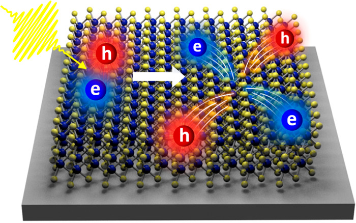
Optical generation of multiple pairs of electrons and holes in semiconductors by an energetic photon (with hυ > 2Eg), a process known as carrier multiplication (CM) or multiexciton generation (MEG),2 provides a novel solution to circumvent the energy losses in hot carriers relevant for high-efficiency photovoltaics. Substantial previous research has aimed at quantifying the CM efficiency and obtaining a fundamental understanding of the CM mechanism with a primary focus on semiconducting quantum dots (QDs).3−11 The benefits from strong quantum confinement for CM in QDs come from the enhanced Coulomb interaction and relaxed momentum conservation condition. On the other hand, previous theoretical12,13 and experimental14−17 studies have also shown that the reduced density of states imposed by confinement may constrain the energy conservation condition so that quantum confinement does not necessarily facilitate CM.
In this context, two-dimensional materials with atomic-level control of the thickness, combined with strong Coulomb effects18,19 and still relatively high density of states, are potentially interesting platforms for efficient CM. Indeed, Aerts et al. reported a strong MEG effect in thin PbS nanosheets with much higher efficiency than that in zero-dimensional QDs, one-dimensional nanorods, and 3D bulk counterparts.20 Furthermore, Kim and colleagues extended recently such studies into multilayered van der Waals (vdW) materials of MoTe2 and WSe2.21 They reported near-perfect MEG in vdW structures employing transient absorption (TA) spectroscopy, that is, a unity quantum yield with an onset energy of 2Eg. However, the mechanism on which the CM/MEG takes place in vdW materials remains elusive. While the generation of multiexcitons following MEG was proposed,21 direct spectroscopic evidence for these high-order excitonic states is missing. Finally, if indeed (multi)excitons are the primary photoproduct, they would have to be dissociated, for example, for photovoltaic applications. Therefore, establishing the nature of the multiple carrier generation process by CM/MEG in vdW structures is relevant for applications.
Results and Discussion
Structural Characterization
Figure 1a shows the atomic configuration of the 2H phase of MoTe2. The sample is produced by chemical vapor deposition (from SixCarbon Technology, Shenzhen), and the layer thickness is about 5 nm (= ∼7 layers). The Raman spectrum in Figure 1b exhibits two prominent peaks at 173 and 235 cm–1 originating from the out-of-plane A1g mode and in-plane E2g mode in 2H-MoTe2.22−24 Optically, multilayered MoTe2 has been shown to possess an indirect bandgap.25 To quantify its bandgap Eg, we have conducted UV–vis absorption measurements. On the basis of the absorbance in Figure 1c, we quantify the bandgap of 2H-MoTe2 to be 0.90 eV using a Tauc plots (see Figure S1). Other optical transitions, marked by A, B, A′, B′, C, and D, correspond to direct transitions at the K and Γ points of the Brillouin zone.26 Note that the absorption of multilayered MoTe2 on sapphire does not show the absorption quanta of ∼1.6% observed by Fang et al. for InAs thin films, presumably due to the indirect nature of transitions in MoTe2.27 For monolayer MoTe2, strong exciton effects have been reported with binding energy up to 600 meV.28−30 For the bulk phase, the exciton binding energy is small at ∼15 meV, substantially lower than the thermal excitation at room temperature (kBT).31
Figure 1.

Characterization of the few-layer 2H-MoTe2 sample. (a) The schematic diagrams of 2H phase structure of MoTe2. (b) Raman spectrum of the 2H-MoTe2 with marks from the computational results.24 (c) UV–vis absorption spectrum of 2H-MoTe2.
Carrier Multiplication in 2H-MoTe2
To explore the CM effect, we employ optical-pump terahertz (THz)-probe (OPTP) spectroscopy to measure the ultrafast photoconductivity. As a purely optical technique, OPTP spectroscopy has been demonstrated to provide quantitative insight into the intrinsic electrical transport properties (including charge density, scattering time, and so forth) in a contact-free manner.32−35 In a typical experiment, as shown in Figure 2a, a laser pulse with tunable photon energies above the bandgap is used to excite electrons from valence to conduction band. Subsequently, a single-cycle THz pulse with ∼1 ps duration is employed to probe the time-dependent photoconductivity (Δσ) dynamics by monitoring the photoinduced THz absorption (ΔE) at varied pump–probe delays. The photoconductivity is proportional to ΔE by Δσ = −ΔE = −(Epump – E0), where Epump and E0 represent the transmitted THz field with and without photoexcitation.
Figure 2.

Investigation of CM in MoTe2 by THz spectroscopy. (a) Schematic illustration of the optical-pump THz-probe spectroscopy. (b) The fluence-dependent, time-resolved THz conductivity following 1.55 eV excitation. The bump at 4 ps originates from re-excitation of the sample by the reflected pulse from the substrate/air interface. (c) The THz conductivities normalized to the absorbed photon density based on the data in (b). (d) Illustration of CM effect by the fluence-dependent THz photoconductivity peak values (left y-axis) and rescaled photogenerated carrier density inferred from the fitting in (e). (e) Frequency-resolved THz conductivity measured with Drude fitting, following excitations of 1.55 and 3.10 eV.
Figure 2b shows the fluence-dependent THz photoconductivity following 1.55 eV excitation. This transient photoconductivity exhibits a subpicosecond rise, reflecting free carrier generation, and a fast decay within a few picoseconds. We attribute this fast decay to ultrafast carrier trapping at defects (see the extended discussion in SI) in line with previous studies.21,36 While the passivation of these defects will be required for device applications, it does not affect the CM process in this study as CM occurs on a subpicosecond time scale.21 In Figure 2c, we present the photoconductivities normalized to the absorbed photon density. We find that within the fluence ranges used in this study, the photoconductivities scale linearly with fluence. On the basis of these results, we can exclude the multiplication of charge carriers trivially by a two-photon excitation process.
To investigate the CM in MoTe2, we have further measured pump photon energy-dependent photoconductivities. The conductivity dynamics following the 3.1 eV excitation is shown in Figure S2a. In Figure 2d, we compare the fluence-dependent peak value in photoconductivity of MoTe2 under 3.1 and 1.55 eV excitations, corresponding to ∼3.4 (CM energetically possible) and 1.7 (CM impossible) times of the bandgap, respectively. For a given absorbed photon density, we find that the photoconductivity upon 3.1 eV excitation is nearly twice that of 1.55 eV excitation. While this photoconductivity multiplication provides a strong indication of possible CM effect in MoTe2, special care needs to be taken for data analysis. Particularly, the photoconductivity Δσ scales with the products of carrier density (N) and charge mobility (μ) as Δσ = N·e·μ with e as the elementary charge. To separate the contribution of the carrier density from the charge mobility, we have conducted THz time-domain spectroscopy (TDS, see SI) at the pump–probe delay close to the photoconductivity peak (at a pump–probe delay of 1.5 ps).
In Figure 2e, we compare the frequency-resolved photoconductivities for both 3.1 and 1.55 eV excitations obtained from TDS measurements. In both cases, the conductivities display a large real conductivity and essentially zero imaginary contribution. This result suggests that a substantial amount (if not all) of photogenerated carriers in our sample are present as free charges. Importantly, the free carrier response dominates the dynamics for all excitations so that we can rule out the free charge generation via “hot exciton dissociation”, one of the most reported free charge generation mechanisms in excitonic materials.37,38
To further shed light on
the electrical transport properties and
disentangle the contribution of carrier density from mobility in MoTe2 at a given pump–probe delay time, we apply the standard
Drude model (see SI).32 We find that the model describes the data well, and we
summarize the inferred parameters in Table 1. When comparing 3.1 and 1.55 eV excitations,
the charge scattering times τ are found to
be nearly identical; the only different parameter is the plasma frequency ωp, which is directly related to carrier
density N. Microscopically, the charge carrier mobility μ in a material is given by  . The same τ for
both 3.1 and 1.55 eV excitations implies that charge carrier mobility
does not depend on the excitation photon energies at the time delay
chosen for TDS (1.5 ps after photoexcitation). To make a quantitative
correlation, we have plotted the carrier densities obtained from the
fittings as the right Y-axis and compared them to
the fluence-dependent photoconductivity data, as shown in Figure 2d. The overlap between
rescaled carrier densities and photoconductivities offers direct,
quantitative evidence for efficient CM taking place in our sample.
Note that the conclusion is robust and does not depend on the model
applied. Strong support for this argument comes from the normalized
frequency-resolved conductivity, as shown in Figure S4 (see SI) based on the same data
sets in Figure 2e,
and we find no observable difference between the two. An extended
analysis based on the Drude–Smith model leads to the same conclusion
of CM (see Figure S5 and associated discussion
in SI). This result also indicates that
charge carriers reach a quasi-equilibrium condition (e.g., at the
band-edge) at 1.5 ps after the excitation with both 1.5 (via cooling
or phonon emission processes) and 3.1 eV (by CM) photons.
. The same τ for
both 3.1 and 1.55 eV excitations implies that charge carrier mobility
does not depend on the excitation photon energies at the time delay
chosen for TDS (1.5 ps after photoexcitation). To make a quantitative
correlation, we have plotted the carrier densities obtained from the
fittings as the right Y-axis and compared them to
the fluence-dependent photoconductivity data, as shown in Figure 2d. The overlap between
rescaled carrier densities and photoconductivities offers direct,
quantitative evidence for efficient CM taking place in our sample.
Note that the conclusion is robust and does not depend on the model
applied. Strong support for this argument comes from the normalized
frequency-resolved conductivity, as shown in Figure S4 (see SI) based on the same data
sets in Figure 2e,
and we find no observable difference between the two. An extended
analysis based on the Drude–Smith model leads to the same conclusion
of CM (see Figure S5 and associated discussion
in SI). This result also indicates that
charge carriers reach a quasi-equilibrium condition (e.g., at the
band-edge) at 1.5 ps after the excitation with both 1.5 (via cooling
or phonon emission processes) and 3.1 eV (by CM) photons.
Table 1. Fitting Parameters for Electrical Charge Transport Properties Based on the Drude Model.
| Drude
model |
||
|---|---|---|
| excitation | ωP (THz) | τ (fs) |
| 1.55 eV | 200 ± 13 | 11 ± 2 |
| 3.10 eV | 279 ± 28 | 10 ± 2 |
Finally, based on the τ inferred from the fittings, we calculate the dc electron mobility in our sample to be 45 ± 9 cm2 V–1 s–1. The value is much higher than that of the QD solids (with the reported value in most studies way below 1 cm2 V–1 s–1 and the highest around 10 cm2 V–1 s–1).39,40 In addition, the estimated mobility is in the same range as the results (∼30–40 cm2 V–1 s–1) from electrical transport measurements on MoTe2 thin films.41,42 As such, we conclude that 2D MoTe2 multilayers uniquely combine efficient CM with high carrier conductivity.
Quantification of CM Efficiency in MoTe2
To evaluate the CM quantum yields, we performed the pump wavelength-dependent OPTP measurements on 2H-MoTe2 with up to 16 different pump photon energies. The conductivity maximum versus fluence is shown in Figure 3a. Here, we take the photoconductivity maximum at a given absorbed photon density (or equivalently the slope in the fluence-dependent conductivity in Figure 3a) to quantify the CM efficiency, as these two values are linked in a linear fashion (see Figure 2d). In Figure 3b, we summarize the photoconductivity normalized to the absorbed photon density at varied photon energies. For the range of excitation energies between 1 and 2 times that of Eg (no CM), we find that the carrier generation efficiency is independent of the pump photon energies, as expected. For further data analysis, we assume the carrier generation quantum yield for photon energy below twice the Eg to be 100% (marked in the right Y-axis). With increasing the photon energy, we observe twice photoconductivity jumps at around 2.8 and 4.2 times of Eg, which we attribute to CM effect following the previous discussion. Remarkably, we observe the enhancement of photoconductivity by CM by a steplike manner with nearly 100% CM quantum yields.43 Finally, we investigate the recombination dynamics following CM. In QD systems, multiple pairs of electrons and holes generated by CM can effectively recombine in a few to tens of picoseconds via Auger recombination.2,8,10,44 In contrast, as shown in Figure S6, for all pump energies used in the study, we observe no changes in the decay dynamics. Apparently, the recombination process is dominated by the fast trapping by defects, which effectively competes with the Auger process. Note that this was previously also concluded by Kim et al.21
Figure 3.

Determination of the carrier-multiplication efficiency. (a) The peak value of THz photoconductivity of 2H-MoTe2 as a function of absorbed photon density for different pump photon energies. The solid lines are linear fittings to the data; three dashed lines represent CM quantum yield of 100%, 200%, and 300%, to guide the eye. (b) The photoconductivity at a given absorbed photon density for varied photon energies (hν, bottom x-axis) and the ratio of hν/Eg (top x-axis). The data are rescaled to match 100% quantum yield of charge generation for the sub-2Eg excitations. The model (dash-dotted lines) is discussed in the main text. (c) Schematic drawing of band structure and carrier multiplication in indirect semiconducting few-layer MoTe2.
Discussion
Now we discuss the mechanism by which CM in multilayer MoTe2 takes place. The free carrier dominant dynamics observed in all pump photon energies implies that CM in our system occurs through a scattering mechanism known as impact ionization (II).12,45−48 In the II process, a hot carrier with excess energy beyond the bandgap can effectively re-excite an additional electron across the bandgap on subpicosecond time scales, driven by carrier–carrier scattering processes. As a reverse Auger recombination process, this model has been previously applied to account for the CM effect in bulk silicon45 and low-dimensional nanomaterials including QDs,12,46,49 carbon nanotubes,50 and 2D materials.47 Within the II framework, the CM efficiency is directly governed by the kinetic competition between II itself and hot carrier cooling. To evaluate the observed CM efficiency and compare the impact ionization rate to the cooling rate, we conduct a further data analysis following a phenomenological model proposed by Beard and colleagues.51 In the model, the detailed band structure of the material is neglected, and the CM efficiency is determined by the II and the carrier cooling via phonon emission.
Comparing the model (shown as dash-dotted lines in Figure 3b) to the data, we find the CM efficiency in 2H-MoTe2 is nearly unity up to ∼94% (see details for the fitting in SI). The CM onset is found to be ∼2.8 Eg. Given the high ηCM, we can readily conclude that the II rate dominates over the cooling process in 2H-MoTe2. Here we estimate the energy loss rate via cooling by (hυ – Eg)/τcooling (with τcooling ∼1.5 ps as the cooling time following 1.55 eV excitation) to be 0.43 eV/ps. We further assume a linear proportionality between the cooling time and the excess energy of hot carriers. Under such an assumption and applying the rate competition model by Beard,51 the II rate is estimated to be nearly 1 order of magnitude higher than the cooling rate for the first CM step (e.g., 3.2 eV/ps for 3.1 eV excitation) to ensure a high CM efficiency in our system. The previously reported CM onset energy in MoTe2 of ∼2 Eg is lower than the 2.8 Eg found here.21 This difference may be due to variations in sample thickness and thus electronic structure but will require further study (see an extended discussion in SI).
While the phenomenological analysis captures the essence of CM, to fully unveil the efficient II and thus CM in 2H-MoTe2 theoretical calculations (e.g., by tight-binding calculations)3,12,46 explicitly on multilayer 2H-MoTe2 are required. To guide future theoretical treatments in this system, we summarize some key observations from the experiments.
(1) CM onset. In our study, the first CM onset and the accompanying sharp rise of the photoconductivity in 2H-MoTe2 is found to be in the range of 2.4–2.6 eV, corresponding to the optical transition at Γ point. To shed further insight on the CM at the Γ point, we discuss the band structure of MoTe2 based on previous theoretical calculation (see a simplified scheme in Figure 3c).52 MoTe2 in excess of three layers exhibits an indirect bandgap involving the K–Λ transition (with Eg 0.90 eV). For the first CM step, while the absorption takes place at Γ point the CM involves the K–Λ transition. Note that the valence band maximum (VBM) at K and Γ points are similar in energy. This results in a favorable “asymmetric” absorption condition, so that most of the excess energy is transferred to hot electrons. In line with our discussion here, Siebbeles et al. have also shown that asymmetric transitions are involved in optical transitions and responsible for the onset of CM effects in PbS QDs and its bulk crystals.3 Overall, the indirect bandgap nature and the relatively close position of VBM at the K and Γ points make energy conservation readily achieved. Note that this characteristic band structure shares similarities with a fictitious band structure proposed by Queisser and his colleagues for optimal CM.45 Finally, to fully understand why CM occurs efficiently at Γ point insights into carrier cooling rate around Γ point are also essential and call for further studies.
(2) Weak electron–phonon coupling in MoTe2. As we discussed, a large rate ratio between II and hot carrier cooling processes kII/kcool is required for efficient CM. Hence, efficient II and slow cooling dynamics favor CM. For the latter process, the weak coupling between the photogenerated hot carriers to phonon modes is desirable. For MoTe2 in both layered and bulk geometries, a few recent studies have reported an intrinsically weak carrier–phonon coupling.53−55 For instance, Makino et al. reported remarkably long-lived optical phonon modes, particularly the A1g mode (with ∼20 ps lifetime) in MoTe2, even in the presence of a large number of photoexcited carriers.55 This observation indicates very week coupling between photogenerated electrons and phonons; in conventional semiconductors (e.g., GaN, ZnO, and so forth), the electron–phonon coupling will lead to the coherent phonon dephasing on ultrafast, picosecond time scale.56,57 The unusual optical phonon dynamics and weak electron–phonon coupling strength could favor the CM by lifting the time constraint for II.
Implication
To illustrate the relevance of CM effect in 2H-MoTe2 for optoelectronics, we compare the CM effect in MoTe2 to that in other extensively studied (e.g., PbS or PbSe systems) or technologically relevant materials (e.g., bulk Si or Si QDs), as shown in Figure 4a. While most of materials possess either only efficient CM (e.g., Si nanocrystals,43 PbS nanosheets,20 and PbSe superlattice solids58) or high carrier mobility (e.g., bulk silicon59), MoTe2 uniquely combines both. This makes layered MoTe2 a fascinating material platform for both fundamental study of CM effect and further device integration. In this context, we further estimate the maximum power conversion efficiency (PCE) for our sample using the detailed balance model as shown in Figure 4b.60,61 In principle, the fast, sub-10 ps trapping process in MoTe2 imposes a challenge for its application in optoelectronics. Effective passivation schemes for the defects have been previously developed for other TMDC materials and should be applicable for MoTe2. For the calculation, we assume that defects can be effectively passivated so that all photogenerated carriers can be efficiently collected. With a quantized band gap of 0.90 eV, the maximum PCE can be reached to 36.8%, increased from 29.5% without CM, with a substantial relative increase of ∼24.7%, illustrating the relevance of CM effect in MoTe2 for optoelectronics.
Figure 4.

(a) CM efficiency comparison among MoTe2 and several other materials. (b) Simulated maximum power conversion efficiency of a MoTe2-based solar cell exposed to an AM1.5 solar spectrum and its comparison to the Shockley–Queisser limit and the ideal CM case.
Conclusions
In summary, we report that efficient photoconductivity or photocurrent multiplication occurs in few-layer 2H-MoTe2 as a direct consequence of an efficient steplike carrier multiplication with near unity quantum yield and extremely high carrier mobility in MoTe2. We demonstrate that free carriers, rather than excitons, are involved in the CM process via impact ionization. The photocurrent multiplication, in conjunction with its ∼1 eV bandgap and easy device integration, thanks to the 2D geometry, makes MoTe2 a promising candidate for hot-carrier related optoelectronics.
Acknowledgments
We thank Heng Zhang, Shuai Fu, Alexander Tries, Xiaoyu Jia, Keno Krewer, Pankaj Seliya, and Paniz Soltani for useful discussions. We acknowledge Ronald Ulbricht and Heejae Kim for constructive comments on the manuscript.
Supporting Information Available
The Supporting Information is available free of charge at https://pubs.acs.org/doi/10.1021/acs.nanolett.0c01693.
Estimating band gap energy Eg using Tauc plots, the origin for the fast decay in carrier dynamics for few-layer MoTe2, photoconductivity dynamics of 2H-MoTe2 with 3.1 eV photoexcitation energy, THz time-domain spectroscopy, fitting the frequency-resolved data by Drude Model, comparison of the normalized frequency-resolved THz conductivity for excitations of 1.55 and 3.1 eV, fitting the frequency-resolved data by Drude–Smith Model, the normalized, pump energy-dependent OPTP dynamics, discussion on CM onset energy difference between our studies and previous studies (PDF)
Author Contributions
H.I.W. designed and supervised the project. W.Z. carried out the experimental work as well as the data analysis. W.Z. and H.I.W. wrote the manuscript. All authors have commented on the manuscript and given approval to the final version of the manuscript.
The authors declare no competing financial interest.
Supplementary Material
References
- Shockley W.; Queisser H. J. Detailed Balance Limit of Efficiency of p-n Junction Solar Cells. J. Appl. Phys. 1961, 32 (3), 510–519. 10.1063/1.1736034. [DOI] [Google Scholar]
- Schaller R. D.; Klimov V. I. High Efficiency Carrier Multiplication in PbSe Nanocrystals: Implications for Solar Energy Conversion. Phys. Rev. Lett. 2004, 92 (18), 186601. 10.1103/PhysRevLett.92.186601. [DOI] [PubMed] [Google Scholar]
- Spoor F. C. M.; Grimaldi G.; Delerue C.; Evers W. H.; Crisp R. W.; Geiregat P.; Hens Z.; Houtepen A. J.; Siebbeles L. D. A. Asymmetric Optical Transitions Determine the Onset of Carrier Multiplication in Lead Chalcogenide Quantum Confined and Bulk Crystals. ACS Nano 2018, 12 (5), 4796–4802. 10.1021/acsnano.8b01530. [DOI] [PMC free article] [PubMed] [Google Scholar]
- Ten Cate S.; Sandeep C. S.; Liu Y.; Law M.; Kinge S.; Houtepen A. J.; Schins J. M.; Siebbeles L. D. Generating Free Charges by Carrier Multiplication in Quantum Dots for Highly Efficient Photovoltaics. Acc. Chem. Res. 2015, 48 (2), 174–181. 10.1021/ar500248g. [DOI] [PubMed] [Google Scholar]
- Sandeep C. S.; Cate S.; Schins J. M.; Savenije T. J.; Liu Y.; Law M.; Kinge S.; Houtepen A. J.; Siebbeles L. D. A. High Charge-Carrier Mobility Enables Exploitation of Carrier Multiplication in Quantum-Dot Films. Nat. Commun. 2013, 4, 2360. 10.1038/ncomms3360. [DOI] [PMC free article] [PubMed] [Google Scholar]
- Mcguire J. A.; Joo J.; Pietryga J. M.; Schaller R. D.; Klimov V. I. New Aspects of Carrier Multiplication in Semiconductor Nanocrystals. Acc. Chem. Res. 2008, 41 (12), 1810–1819. 10.1021/ar800112v. [DOI] [PubMed] [Google Scholar]
- Schaller R. D.; Agranovich V. M.; Klimov V. I. High-Efficiency Carrier Multiplication through Direct Photogeneration of Multi-Excitons via Virtual Single-Exciton States. Nat. Phys. 2005, 1 (3), 189–194. 10.1038/nphys151. [DOI] [Google Scholar]
- Trinh M. T.; Houtepen A. J.; Schins J. M.; Hanrath T.; Piris J.; Knulst W.; Goossens A. P. L. M.; Siebbeles L. D. A. Spite of Recent Doubts Carrier Multiplication Does Occur in PbSe Nanocrystals. Nano Lett. 2008, 8 (6), 1713–1718. 10.1021/nl0807225. [DOI] [PubMed] [Google Scholar]
- Trinh M. T.; Polak L.; Schins J. M.; Houtepen A. J.; Vaxenburg R.; Maikov G. I.; Grinbom G.; Midgett A. G.; Luther J. M.; Beard M. C.; Nozik A. J.; Bonn M.; Lifshitz E.; Siebbeles L. D. A. Anomalous Independence of Multiple Exciton Generation on Different Group IV-VI Quantum Dot Architectures. Nano Lett. 2011, 11 (4), 1623–1629. 10.1021/nl200014g. [DOI] [PubMed] [Google Scholar]
- Beard M. C.; Knutsen K. P.; Yu P.; Luther J. M.; Song Q.; Metzger W. L.; Ellingson R. J.; Nozik A. J. Multiple Exciton Generation in Colloidal Silicon Nanocrystals. Nano Lett. 2007, 7 (8), 2506–2512. 10.1021/nl071486l. [DOI] [PubMed] [Google Scholar]
- Beard M. C.; Midgett A. G.; Law M.; Semonin O. E.; Ellingson R. J.; Nozik A. J. Variations in the Quantum Efficiency of Multiple Exciton Generation for a Series of Chemically Treated PbSe Nanocrystal Films. Nano Lett. 2009, 9 (2), 836–845. 10.1021/nl803600v. [DOI] [PubMed] [Google Scholar]
- Allan G.; Delerue C. Role of Impact Ionization in Multiple Exciton Generation in PbSe Nanocrystals. Phys. Rev. B: Condens. Matter Mater. Phys. 2006, 73 (20), 205423. 10.1103/PhysRevB.73.205423. [DOI] [Google Scholar]
- Delerue C.; Allan G.; Pijpers J. J. H.; Bonn M. Carrier Multiplication in Bulk and Nanocrystalline Semiconductors: Mechanism, Efficiency, and Interest for Solar Cells. Phys. Rev. B: Condens. Matter Mater. Phys. 2010, 81 (12), 125306. 10.1103/PhysRevB.81.125306. [DOI] [Google Scholar]
- Pijpers J. J. H.; Ulbricht R.; Tielrooij K. J.; Osherov A.; Golan Y.; Delerue C.; Allan G.; Bonn M. Assessment of Carrier-Multiplication Efficiency in Bulk PbSe and PbS. Nat. Phys. 2009, 5 (11), 811–814. 10.1038/nphys1393. [DOI] [Google Scholar]
- Ben-Lulu M.; Mocatta D.; Bonn M.; Banin U.; Ruhman S. On the Absence of Detectable Carrier Multiplication in a Transient Absorption Study of InAs/CdSe/ZnSe Core/Shell1/ Shell2 Quantum Dots. Nano Lett. 2008, 8 (4), 1207–1211. 10.1021/nl080199u. [DOI] [PubMed] [Google Scholar]
- Nair G.; Bawendi M. G. Carrier Multiplication Yields of CdSe and CdTe Nanocrystals by Transient Photoluminescence Spectroscopy. Phys. Rev. B: Condens. Matter Mater. Phys. 2007, 76 (8), 081304. 10.1103/PhysRevB.76.081304. [DOI] [Google Scholar]
- Nair G.; Geyer S. M.; Chang L. Y.; Bawendi M. G. Carrier Multiplication Yields in PbS and PbSe Nanocrystals Measured by Transient Photoluminescence. Phys. Rev. B: Condens. Matter Mater. Phys. 2008, 78 (12), 125325. 10.1103/PhysRevB.78.125325. [DOI] [Google Scholar]
- Mak K. F.; Lee C.; Hone J.; Shan J.; Heinz T. F. Atomically Thin MoS2: a New Direct-Gap Semiconductor. Phys. Rev. Lett. 2010, 105 (13), 136805. 10.1103/PhysRevLett.105.136805. [DOI] [PubMed] [Google Scholar]
- Mak K. F.; He K.; Lee C.; Lee G. H.; Hone J.; Heinz T. F.; Shan J. Tightly Bound Trions in Monolayer MoS2. Nat. Mater. 2013, 12 (3), 207–211. 10.1038/nmat3505. [DOI] [PubMed] [Google Scholar]
- Aerts M.; Bielewicz T.; Klinke C.; Grozema F. C.; Houtepen A. J.; Schins J. M.; Siebbeles L. D. A. Highly Efficient Carrier Multiplication in PbS Nanosheets. Nat. Commun. 2014, 5, 3789. 10.1038/ncomms4789. [DOI] [PMC free article] [PubMed] [Google Scholar]
- Kim J. H.; Bergren M. R.; Park J. C.; Adhikari S.; Lorke M.; Frauenheim T.; Choe D. H.; Kim B.; Choi H.; Gregorkiewicz T.; Lee Y. H. Carrier Multiplication in Van Der Waals Layered Transition Metal Dichalcogenides. Nat. Commun. 2019, 10 (1), 5488. 10.1038/s41467-019-13325-9. [DOI] [PMC free article] [PubMed] [Google Scholar]
- Tan Y.; Luo F.; Zhu M.; Xu X.; Ye Y.; Li B.; Wang G.; Luo W.; Zheng X.; Wu N.; Yu Y.; Qin S.; Zhang X. A. Controllable 2H-to-1T’ Phase Transition in Few-Layer MoTe2. Nanoscale 2018, 10 (42), 19964–19971. 10.1039/C8NR06115G. [DOI] [PubMed] [Google Scholar]
- Kan M.; Nam H. G.; Lee Y. H.; Sun Q. Phase Stability and Raman Vibration of the Molybdenum Ditelluride (MoTe2) Monolayer. Phys. Chem. Chem. Phys. 2015, 17 (22), 14866–14871. 10.1039/C5CP01649E. [DOI] [PubMed] [Google Scholar]
- Empante T. A.; Zhou Y.; Klee V.; Nguyen A. E.; Lu I. H.; Valentin M. D.; Alvillar S. A. N.; Preciado E.; Berges A. J.; Merida C. S.; Gomez M.; Bobek S.; Isarraraz M.; Reed E. J.; Bartels L. Chemical Vapor Deposition Growth of Few-Layer MoTe2 in the 2H, 1T’, and 1T Phases: Tunable Properties of MoTe2 Films. ACS Nano 2017, 11 (1), 900–905. 10.1021/acsnano.6b07499. [DOI] [PubMed] [Google Scholar]
- Ruppert C.; Aslan O. B.; Heinz T. F. Optical Properties and Band Gap of Single- and Few-Layer MoTe2 Crystals. Nano Lett. 2014, 14 (11), 6231–6236. 10.1021/nl502557g. [DOI] [PubMed] [Google Scholar]
- Wilson J. A.; Yoffe A. D. The Transition Metal Dichalcogenides Discussion and Interpretation of the Observed Optical, Electrical and Structural Properties. Adv. Phys. 1969, 18 (73), 193–335. 10.1080/00018736900101307. [DOI] [Google Scholar]
- Fang H.; Bechtel H. A.; Plis E.; Martin M. C.; Krishna S.; Yablonovitch E.; Javey A. Quantum of Optical Absorption in Two-Dimensional Semiconductors. Proc. Natl. Acad. Sci. U. S. A. 2013, 110 (29), 11688–11691. 10.1073/pnas.1309563110. [DOI] [PMC free article] [PubMed] [Google Scholar]
- Yang J.; Lu T.; Myint Y. W.; Pei J.; Macdonald D.; Zheng J. C.; Lu Y. Robust Excitons and Trions in Monolayer MoTe2. ACS Nano 2015, 9 (6), 6603–6609. 10.1021/acsnano.5b02665. [DOI] [PubMed] [Google Scholar]
- Robert C.; Picard R.; Lagarde D.; Wang G.; Echeverry J. P.; Cadiz F.; Renucci P.; Högele A.; Amand T.; Marie X.; Gerber I. C.; Urbaszek B. Excitonic Properties of Semiconducting Monolayer and Bilayer MoTe2. Phys. Rev. B: Condens. Matter Mater. Phys. 2016, 94 (15), 155425. 10.1103/PhysRevB.94.155425. [DOI] [Google Scholar]
- Han B.; Robert C.; Courtade E.; Manca M.; Shree S.; Amand T.; Renucci P.; Taniguchi T.; Watanabe K.; Marie X.; Golub L. E.; Glazov M. M.; Urbaszek B. Exciton States in Monolayer MoSe2 and MoTe2 Probed by Upconversion Spectroscopy. Phys. Rev. X 2018, 8 (3), 031073. 10.1103/PhysRevX.8.031073. [DOI] [Google Scholar]
- Sun Y.; Zhang J.; Ma Z.; Chen C.; Han J.; Chen F.; Luo X.; Sun Y.; Sheng Z. The Zeeman Splitting of Bulk 2H-MoTe2 Single Crystal in High Magnetic Field. Appl. Phys. Lett. 2017, 110 (10), 102102. 10.1063/1.4977953. [DOI] [Google Scholar]
- Ulbricht R.; Hendry E.; Shan J.; Heinz T. F.; Bonn M. Carrier Dynamics in Semiconductors Studied with Time-Resolved Terahertz Spectroscopy. Rev. Mod. Phys. 2011, 83 (2), 543–586. 10.1103/RevModPhys.83.543. [DOI] [Google Scholar]
- Dong R.; Han P.; Arora H.; Ballabio M.; Karakus M.; Zhang Z.; Shekhar C.; Adler P.; Petkov P. S.; Erbe A.; Mannsfeld S. C. B.; Felser C.; Heine T.; Bonn M.; Feng X.; Canovas E. High-Mobility Band-Like Charge Transport in a Semiconducting Two-Dimensional Metal-Organic Framework. Nat. Mater. 2018, 17 (11), 1027–1032. 10.1038/s41563-018-0189-z. [DOI] [PubMed] [Google Scholar]
- Tomadin A.; Hornett S. M.; Wang H. I.; Alexeev E. M.; Candini A.; Coletti C.; Turchinovich D.; Kläui M.; Bonn M.; Koppens F. H. L.; Hendry E.; Polini M.; Tielrooij K. J. The Ultrafast Dynamics and Conductivity of Photoexcited Graphene at Different Fermi Energies. Sci. Adv. 2018, 4 (5), eaar5313. 10.1126/sciadv.aar5313. [DOI] [PMC free article] [PubMed] [Google Scholar]
- Xu F.; Yu C.; Tries A.; Zhang H.; Klaui M.; Basse K.; Hansen M. R.; Bilbao N.; Bonn M.; Wang H. I.; Mai Y. Tunable Superstructures of Dendronized Graphene Nanoribbons in Liquid Phase. J. Am. Chem. Soc. 2019, 141 (28), 10972–10977. 10.1021/jacs.9b04927. [DOI] [PubMed] [Google Scholar]
- Ghimire M. K.; Ji H.; Gul H. Z.; Yi H.; Jiang J.; Lim S. C. Defect-Affected Photocurrent in MoTe2 FETs. ACS Appl. Mater. Interfaces 2019, 11 (10), 10068–10073. 10.1021/acsami.9b00050. [DOI] [PubMed] [Google Scholar]
- Grancini G.; Maiuri M.; Fazzi D.; Petrozza A.; Egelhaaf H. J.; Brida D.; Cerullo G.; Lanzani G. Hot Exciton Dissociation in Polymer Solar Cells. Nat. Mater. 2013, 12 (1), 29–33. 10.1038/nmat3502. [DOI] [PubMed] [Google Scholar]
- Tries A.; Osella S.; Zhang P.; Xu F.; Ramanan C.; Klaui M.; Mai Y.; Beljonne D.; Wang H. I. Experimental Observation of Strong Exciton Effects in Graphene Nanoribbons. Nano Lett. 2020, 20 (5), 2993–3002. 10.1021/acs.nanolett.9b04816. [DOI] [PMC free article] [PubMed] [Google Scholar]
- Evers W. H.; Schins J. M.; Aerts M.; Kulkarni A.; Capiod P.; Berthe M.; Grandidier B.; Delerue C.; van der Zant H. S. J.; van Overbeek C.; Peters J. L.; Vanmaekelbergh D.; Siebbeles L. D. A. High Charge Mobility in Two-Dimensional Percolative Networks of PbSe Quantum Dots Connected by Atomic Bonds. Nat. Commun. 2015, 6, 8195. 10.1038/ncomms9195. [DOI] [PMC free article] [PubMed] [Google Scholar]
- Lan X.; Chen M.; Hudson M. H.; Kamysbayev V.; Wang Y.; Guyot-Sionnest P.; Talapin D. V. Quantum Dot Solids Showing State-Resolved Band-Like Transport. Nat. Mater. 2020, 19 (3), 323–329. 10.1038/s41563-019-0582-2. [DOI] [PubMed] [Google Scholar]
- Pradhan N. P.; Rhodes D.; Feng X.; Xin Y.; Memaran S.; Moon B.-H.; Terrones H.; Terrones M.; Balicas L. Field-Effect Transistors Based on Few-Layered α-MoTe2. ACS Nano 2014, 8 (6), 5911–5920. 10.1021/nn501013c. [DOI] [PubMed] [Google Scholar]
- Keum D. H.; Cho S.; Kim J. H.; Choe D. H.; Sung H. J.; Kan M.; Kang H.; Hwang J. Y.; Kim S. W.; Yang H.; Chang K. J.; Lee Y. H. Bandgap Opening in Few–Layered Monoclinic MoTe2. Nat. Phys. 2015, 11 (6), 482–486. 10.1038/nphys3314. [DOI] [Google Scholar]
- Timmerman D.; Valenta J.; Dohnalova K.; de Boer W. D. A. M.; Gregorkiewicz T. Step–Like Enhancement of Luminescence Quantum Yield of Silicon Nanocrystals. Nat. Nanotechnol. 2011, 6 (11), 710–713. 10.1038/nnano.2011.167. [DOI] [PubMed] [Google Scholar]
- Binks D. J. Multiple Exciton Generation in Nanocrystal Quantum Dots--Controversy, Current Status and Future Prospects. Phys. Chem. Chem. Phys. 2011, 13 (28), 12693–12704. 10.1039/c1cp20225a. [DOI] [PubMed] [Google Scholar]
- Werner J. H.; Kolodinski S.; Queisser H. J. Novel Optimization Principles and Efficiency Limits for Semiconductor Solar Cells. Phys. Rev. Lett. 1994, 72 (24), 3851–3854. 10.1103/PhysRevLett.72.3851. [DOI] [PubMed] [Google Scholar]
- Franceschetti A.; An J. M.; Zunger A. Impact Ionization Can Explain Carrier Multiplication in PbSe Quantum Dots. Nano Lett. 2006, 6 (10), 2191–2195. 10.1021/nl0612401. [DOI] [PubMed] [Google Scholar]
- Michael S.; Schneider H. C. Impact Ionization Dynamics in Small Band-Gap Two-Dimensional Materials from a Coherent Phonon Mechanism. Phys. Rev. B: Condens. Matter Mater. Phys. 2019, 100 (3), 035431. 10.1103/PhysRevB.100.035431. [DOI] [Google Scholar]
- Baer R.; Rabani E. Can Impact Excitation Explain Efficient Carrier Multiplication in Carbon Nanotube Photodiodes?. Nano Lett. 2010, 10 (9), 3277–3282. 10.1021/nl100639h. [DOI] [PubMed] [Google Scholar]
- Califano M.; Zunger A.; Franceschetti A. Direct Carrier Multiplication due to Inverse Auger Scattering in CdSe Quantum Dots. Appl. Phys. Lett. 2004, 84 (13), 2409–2411. 10.1063/1.1690104. [DOI] [Google Scholar]
- Gabor N. M.; Zhong Z.; Bosnick K.; Park J.; McEuen P. L. Extremely Efficient Multiple Electron-Hole Pair Generation in Carbon Nanotube Photodiodes. Science 2009, 325, 1367–1371. 10.1126/science.1176112. [DOI] [PubMed] [Google Scholar]
- Beard M. C.; Midgett A. G.; Hanna M. C.; Luther J. M.; Hughes B. K.; Nozik A. J. Comparing Multiple Exciton Generation in Quantum Dots to Impact Ionization in Bulk Semiconductors: Implications for Enhancement of Solar Energy Conversion. Nano Lett. 2010, 10 (8), 3019–3027. 10.1021/nl101490z. [DOI] [PubMed] [Google Scholar]
- Sun Y.; Wang D.; Shuai Z. Indirect-to-Direct Band Gap Crossover in Few-Layer Transition Metal Dichalcogenides: A Theoretical Prediction. J. Phys. Chem. C 2016, 120 (38), 21866–21870. 10.1021/acs.jpcc.6b08748. [DOI] [Google Scholar]
- Li T.; Zhang Z.; Zheng W.; Lv Y.; Huang F. A Possible High-Mobility Signal in Bulk MoTe2: Temperature Independent Weak Phonon Decay. AIP Adv. 2016, 6 (11), 115207. 10.1063/1.4967351. [DOI] [Google Scholar]
- Helmrich S.; Schneider R.; Achtstein A. W; Arora A.; Herzog B.; de Vasconcellos S. M.; Kolarczik M.; Schops O.; Bratschitsch R.; Woggon U.; Owschimikow N. Exciton–Phonon Coupling in Mono- and Bilayer MoTe2. 2D Mater. 2018, 5 (4), 045007. 10.1088/2053-1583/aacfb7. [DOI] [Google Scholar]
- Makino K.; Saito Y.; Horii S.; Fons P.; Kolobov A. V.; Ando A.; Ueno K.; Mondal R.; Hase M.. Ultrafast Dynamics of Electron-Phonon Coupling in Transition-Metal Dichalcogenides. 2018, arXiv:1807.10879. Cond. Mat. Mtrl. Sci., https://arxiv.org/abs/1807.10879 (accessed Sep. 16 2019). [Google Scholar]
- Yee K. J.; Lee K. G.; Oh E.; Kim D. S.; Lim Y. S. Coherent Optical Phonon Oscillations in Bulk GaN Excited by Far below the Band Gap Photons. Phys. Rev. Lett. 2002, 88 (10), 105501. 10.1103/PhysRevLett.88.105501. [DOI] [PubMed] [Google Scholar]
- Ishioka K.; Petek H.; Kaydashev V. E.; Kaidashev E. M.; Misochko O. V. Coherent Optical Phonons of ZnO under Near Resonant Photoexcitation. J. Phys.: Condens. Matter 2010, 22 (46), 465803. 10.1088/0953-8984/22/46/465803. [DOI] [PubMed] [Google Scholar]
- Kulkarni A.; Evers W. H.; Tomic S.; Beard M. C.; Vanmaekelbergh D.; Siebbeles L. D. A. Efficient Steplike Carrier Multiplication in Percolative Networks of Epitaxially Connected PbSe Nanocrystals. ACS Nano 2018, 12 (1), 378–384. 10.1021/acsnano.7b06511. [DOI] [PMC free article] [PubMed] [Google Scholar]
- Wolf M.; Brendel R.; Werner J. H.; Queisser H. J. Solar Cell Efficiency and Carrier Multiplication in Si1–xGex Alloys. J. Appl. Phys. 1998, 83 (8), 4213–4221. 10.1063/1.367177. [DOI] [Google Scholar]
- Hanna M. C.; Nozik A. J. Solar Conversion Efficiency of Photovoltaic and Photoelectrolysis Cells with Carrier Multiplication Absorbers. J. Appl. Phys. 2006, 100, 074510. 10.1063/1.2356795. [DOI] [Google Scholar]
- Jensen S. A.; Versluis J.; Cánovas E.; Pijpers J. J. H.; Sellers I. R.; Bonn M. Carrier Multiplication in Bulk Indium Nitride. Appl. Phys. Lett. 2012, 101 (22), 222113. 10.1063/1.4766738. [DOI] [Google Scholar]
Associated Data
This section collects any data citations, data availability statements, or supplementary materials included in this article.