Abstract
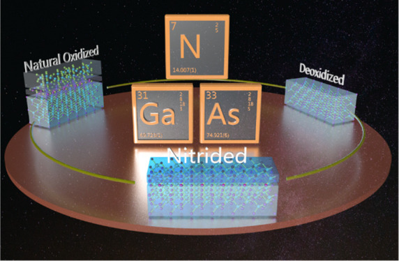
As one of the successful approaches to GaAs surface passivation, wet-chemical nitridation is applied here to relate the effect of surface passivation to carrier recombination processes in bulk GaAs. By combining time-resolved photoluminescence and optical pump—THz probe measurements, we found that surface hole trapping dominates the decay of photoluminescence, while photoconductivity dynamics is limited by surface electron trapping. Compared to untreated sample dynamics, the optimized nitridation reduces hole- and electron-trapping rate by at least 2.6 and 3 times, respectively. Our results indicate that under ambient conditions, recovery of the fast hole trapping due to the oxide regrowth at the deoxidized GaAs surface takes tens of hours, while it is effectively inhibited by surface nitridation. Our study demonstrates that surface nitridation stabilizes the GaAs surface via reduction of both electron- and hole-trapping rates, which results in chemical and electronical passivation of the bulk GaAs surface.
Keywords: GaAs, time-resolved spectroscopy, charge trapping, surface passivation, surface recombination velocity
Introduction
Bulk GaAs crystals with their direct band gap and high electron mobility have extensive applications in electronic and optoelectronic devices.1−4 The development of the GaAs technology has been impeded by high density of surface states on GaAs. At ambient conditions, on the surface of bulk GaAs, an oxide layer is formed, which is expected to lead to charge trapping.5,6 Charge trapping reduces free carrier lifetime and worsens electronic properties of devices. In addition, the oxide layer is physically unstable and could be corroded over time, which would degrade the performance of devices.7 To improve the performance achieved by the state-of-the-art GaAs-based optoelectronic devices, efficient surface passivation could be the key factor.
Over the past years, a variety of methods have been developed for passivating the GaAs surface.8−11 One conventional but technologically demanding method is an epitaxial growth of a high band gap layer, such as AlGaAs, GaP, Al2O3, and GaN on the GaAs surface.12−16 The high band gap layers could reduce the surface trap density and thus reduce photoluminescence (PL) decay rate15,17,18 and improve the performance of GaAs-based devices.19−21 Chemical passivation, such as sulfidation and nitridation by wet chemistry, is another typical and inexpensive passivation approach.9,22−24 Sulfidation of the surface by wet chemistry improves the efficiency of solar cells.24,25 However, the sulfide layer is unstable at ambient conditions, and a protective layer is needed to prevent the sulfide layer’s degradation.26 Surface nitridation by hydrazine sulfide solution can form a GaN monolayer at the GaAs surface. This monolayer can protect the crystal surface against oxidation over a period of months and significantly improve the GaAs optical and electrical properties.17,26−28 Overall, surface nitridation is a stable and effective method for passivation of the GaAs surface. However, a comprehensive description of processes influenced by nitride passivation, in particular carrier recombination processes, is not yet available.
The ultimate way to evaluate surface passivation is to quantify its effect on the performance of the device of interest. However, the production and characterization of devices are usually nontrivial. Therefore, it is desirable to develop an approach to evaluate the effect of surface passivation on charge carrier dynamics prior to device manufacturing. Steady-state and time-resolved spectroscopy are well-accepted characterization methods that can provide a detailed description of the processes within the materials of interest.29,30 In particular, PL quantum yield (PLQY) measurement is a useful steady-state technique that is naturally coupled with the description of the thermodynamic limit of photovoltage in photovoltaics.31,32
In this work, we studied the effect of surface nitridation on carrier recombination dynamics in GaAs crystals by means of time-resolved photoinduced luminescence (TRPL) and optical pump—THz probe (TRTS) techniques. Furthermore, from PLQY measurements, we found that surface nitridation significantly reduces the density of nonradiative trapping centers as compared to naturally oxidized and HCl solution-processed GaAs surfaces. By comparing TRPL and TRTS kinetics, we concluded that surface hole-trapping process quenches radiative recombination, while surface electron trapping dominates photoconductivity dynamics. We found that the best-effort nitridation as compared to the sample with surface oxides can reduce hole- and electron-trapping rates by a factor of 2.6 and 3, respectively. After native oxides were removed using HCl solution, which is complemented by an increase in the TRPL decay time, we observed PL decay time shortening over tens of hours toward the level measured in naturally oxidized GaAs, most probably because of a surprisingly slow formation of the new oxide layer on the surface of GaAs. On the contrary, within 100 h, we observed no change in TRPL decay time in GaAs after nitridation, proving that GaAs surface after nitridation effectively prevents the oxide regrowth. These results demonstrate that nitridation does stabilize the GaAs surface and reduce both electron- and hole-trapping rates.
Results and Discussion
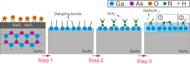
We modified the GaAs (unintentionally doped) surface according to the following procedures. For nitridation of the GaAs (100) wafer, it was immersed in a low-alkaline hydrazine sulfide solution (pH ≈ 8.5, 80 οC) for 10 min. After that, the sample was rinsed by deionized (DI) water and then dried in nitrogen. As a result of nitridation, a thin GaN1–xAsx layer was formed on the GaAs surface. The schematic descriptions of the nitridation reactions are shown in Figure 1. In step 1, HCl in alkaline hydrazine sulfide solution reacts with the native oxides, such as Ga2O3, As2O5, and As2O3,33,34 which is expected to lead to formation of dangling bonds on the GaAs surface. In step 2, electrophilic adsorption centers are formed on the oxide-free surface via electron transfer from the conduction band of GaAs to (N2H5)+ or H3O+ in the solutions, and the surface dangling bonds are terminated. Further selective reaction of SH– anions with the surface arsenic forms thioarsenic acid, H3AsO4, that is easily rinsed away, resulting in Ga-terminated (100).35,36 In step 3, a GaN1–xAsx layer is formed on the surface via the interaction between two N dangling bonds (① in Figure 1) or via the reaction between N dangling bonds and H2O (② in Figure 1). The composition of As in the layer (x) was estimated from the correlation between the emission peak energy and x (Supporting Information) and found to be <0.06.37 For surface deoxidation, a precleaned GaAs wafer was dipped into a 1 M HCl (Sigma-Aldrich, 37%) water solution for 30 s at room temperature and then rinsed with DI water before being dried in nitrogen. After removing surface oxides using HCl, the surface of GaAs is expected to be terminated by chlorine atoms.38,39 A detailed description of the sample preparation, TRPL, TRTS, and PLQY measurements can be found in the Supporting Information.
Figure 1.
Schematic of surface nitridation reactions at the GaAs surface.
Then, we spectroscopically characterized the modified surface in comparison to the native oxidized and deoxidized form. First, we examined the time-integrated PL emission of GaAs wafers with surfaces treated differently, as shown in Figure 2. We observed that the time-integrated PL intensity of the deoxidized wafer is about 2.5 times greater than that of the naturally oxidized samples. After nitridation, we observed further increase in the PL intensity, which is 3 times greater than for the chlorine-terminated and 7.5 times greater than for the naturally oxidized samples, indicating that surface nitridation can further reduce the concentration of surface trap centers.
Figure 2.
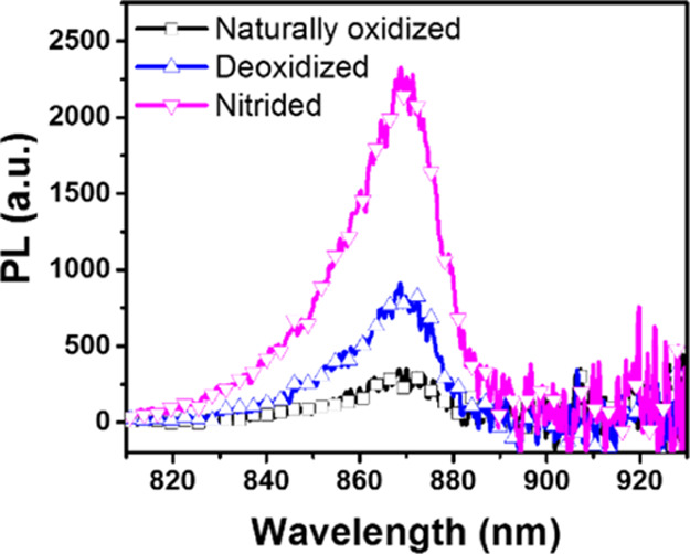
Time-integrated PL spectra of GaAs wafers naturally oxidized, deoxidized, and after 10 min nitridation treatment under photoexcitation at 1.6 eV. The excitation photon flux was 1.9 × 10¹³ photons cm–2 pulse–1 for these PL spectra measurements.
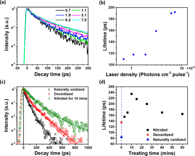
To understand the underlying mechanisms of carrier recombination, we analyzed TRPL kinetics. Figure 3a shows TRPL kinetics of 10 min nitride-treated GaAs under varied excitation photon flux. We observed that TRPL decays slower with increasing excitation power. A similar phenomenon was observed for GaAs having naturally oxidized and deoxidized surfaces (Supporting Information). To rationalize this observation, we should consider all mechanisms of charge recombination. In general, PL in semiconductors is emitted when mobile electrons and holes encounter each other and undergo radiative recombination. In GaAs, the decay of photogenerated mobile carrier concentration can be induced by radiative recombination of mobile electrons and holes, nonradiative Auger recombination, and trap-assisted nonradiative charge recombination having traps formed by defects, impurities, and dangling bonds.40−42 Furthermore, separation of mobile electrons and holes in space so that they do not encounter each other should also lead to reduction in the radiative recombination rate. Such spatial separation may occur under an influence of an electric field gradient, for example, because of the surface pinning effect.43 It is important to note that although separated in space, photogenerated charges remain mobile; thus, their recombination while being slowed down will be of the radiative character.
Figure 3.
(a) Normalized TRPL kinetics and (b) PL decay times of GaAs after 10 min nitridation under varied excitation fluencies from 0.7 to 7.0 × 10¹³ photons cm–2 pulse–1 at 1.6 eV. (c) Normalized TRPL kinetics and (d) PL decay times of the GaAs wafer after having been naturally oxidized, deoxidized, and nitrided with varying nitridation times. The excitation photon energy and flux were 1.6 eV and 1.9 × 10¹³ photons cm–2 pulse–1, respectively. Solid lines are the fitting curves based on double-exponential functions. The fitting parameters are given in the Supporting Information. In the Figure 3(b,d), TRPL decay time is quantified via 1/e methods.
The radiative recombination of mobile charges is a bimolecular (second-order) process, which is dependent on the product of concentrations of mobile electrons and holes, thus on the square of the concentration of absorbed excitation photons, and thus on the square of the incident photon flux. Furthermore, Auger recombination is dependent on the third power of the flux. Therefore, both Auger recombination and radiative recombination processes should lead to a faster PL decay with increasing concentration of photogenerated charges under increased excitation power if the decay is dominated by these processes. This expectation is opposite to that of what we observed in the experiment. On the contrary, the decay of PL dominated by charge trapping under an excessive amount of traps should not speed up as this process is of the first order. Thus, TRPL kinetics in our case is most likely dominated by the charge-trapping processes. At high injection, a unique type of excessive traps should lead to a first-order rate equation with an exponential decay function. We note that PL exhibits a nonexponential decay in all three samples. This nonexponential PL dynamics may be related to inhomogeneous distribution of trap energy and thus, trapping rates in the samples. Also, two channels of PL reduction due to charge trapping and spatial separation could be responsible for different PL decay rates, thus leading to a two-exponential appearance of the decay. Further, the observed slowing down of the PL decay, if dominated by charge trapping, can be understood via trap filling. Indeed, at low fluence, charge carriers are efficiently captured by empty traps. This leads to a fast PL decay. With increasing fluence, some traps are filled by photogenerated charges at the arrival of the next excitation pulse. Consequently, the charge-trapping rate decreases and PL decays slower.
On the other hand, at low injection, the role of spatial separation of charges due to surface pinning could be also substantial.44 With increase in the injection level, the contribution of the charge separation induced by the surface electric field will decrease as charges of a certain polarity will compensate the surface field. Consequently, the contribution of the early PL decay induced by the charge separation in the surface pinning-induced electric field will decrease. At the same time, on a longer timescale, mobile charges should recombine easily, and the long-time PL decay should speed up. Thus, the observed dependency of the PL decay on the excitation intensity does not agree with the dominance of the surface pinning effect.
Furthermore, we can discriminate the role of charge trapping and spatial separation in the PL dynamics, considering the overall efficiency of steady-state PL. For that, we measure an absolute PLQY defined as the ratio of the number of emitted photons to the number of absorbed photons (Supporting Information). As pointed out above, spatial separation of photogenerated charges should not reduce QY but rather delay the PL decay. Nevertheless, for all studied samples, we record QY at the level of one percent, suggesting that nonradiative recombination of charges is the dominant process.
For simplified quantification of the nonexponential PL dynamics, we consider the time it takes for the emission intensity to decay to 1/e of its initial value, as shown in Figure 3b,d. We find that at the fluency of 1.9 × 10¹³ photons cm–2 pulse–1 after 1.6 eV excitation, PL lifetime of GaAs after the best nitridation (see below) is ∼225 ps, which is 1.6 times longer than that for the deoxidized GaAs (∼140 ps) and 2.8 times longer than that for the naturally oxidized sample (∼80 ps). Further, we find that PL decay time of the nitrided GaAs depends on the nitridation time: PL decays slower with increasing nitridation time until 10 min, and with a further increase in the nitridation time, the PL decay speeds up (Figure 3c,d). This observation can be rationalized as follows. Naturally, a certain nitridation time is required to fully convert the GaAs surface.27 On the other hand, SH– anions could incorporate into the chemisorbed layer upon longer nitridation and break the short-range order of the overlayer,35 which could create new trapping centers. Moreover, the formation of a thick GaN layer upon longer nitridation may induce strain on the surface of the GaAs wafer because of the high GaAs/GaN lattice mismatch.27 Such strain could create defects that would function as new trapping centers. Thus, from our TRPL measurements, we see that ∼10 min of nitridation time is optimal for balancing these two mechanisms. The observed dependency suggests a requirement of careful optimization of the surface nitridation procedure for obtaining an efficient GaN passivation layer for GaAs.
It is useful to compare the PL passivation effect evaluated by different approaches. Naturally, time-integrated TRPL spectra represent relative QY measurements; thus, the ratio of intensity of integrated spectra [1 (naturally oxidized): 2.5 (HCl-treated): 7.5 (best nitridation)] is expected to agree with the ratio of the absolute QY values (1:1.6:2.6). We associate the mismatch of these values with the different types of excitation: 80 MHz short pulse in time-integrated TRPL spectra and continuous wave in the case of absolute QY. Most probably, much more intense short-pulse excitation leads to filling of some traps out of their distribution, whereas others are still active. We interpret our results such that both surface deoxidation and nitridation have a stronger passivating effect on the nonfilled traps. Also, when we compare the changes in intensities of time-integrated spectra and of time-resolved PL decays, we notice more pronounced passivation effect on time-integrated spectra. Evidently, if the entire PL dynamics was resolved in TRPL measurements, integrated spectra should be proportional to the decay dynamics. We associate the observed difference with the PL decay, which was not resolved in the experiment. The temporal resolution of the streak-camera is about 2 ps, and this implies that a faster PL decay process, which apparently can be passivated more efficiently, could be responsible for our observations.
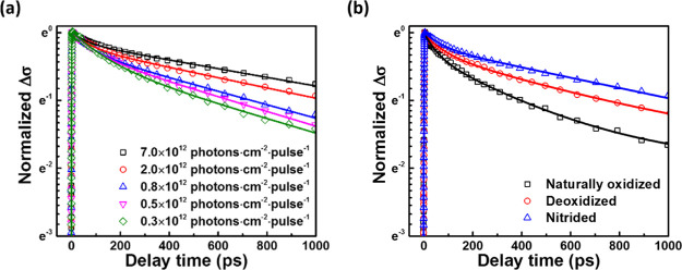
As compared to TRPL where either electron and hole trapping or both may influence the decays,40,41 TRTS is selectively sensitive to time-dependent photoconductivity Δσ(t) of the sample and hence to the product of carrier mobility μ and the concentration of mobile photogenerated charges.45 For GaAs, electron mobility (μe) is significantly higher than hole mobility (μh);46−48 thus, we presume that Δσ(t) is mainly related to photogenerated electrons. Figure 4a shows TRTS kinetics of nitrided GaAs under varying excitation fluence. Apparently, Δσ(t) decays nonexponentially, and the decay slows down with increasing excitation fluence. Similar trends were also observed for naturally oxidized and deoxidized GaAs (Supporting Information). The slowing down of the Δσ(t) decay with increased excitation allows us to conclude that, similar to TRPL results, the nonlinear recombination processes such as bimolecular radiative and the third-order Auger recombination do not dominate the observed dynamics.
Figure 4.
(a) Normalized photoconductivity (Δσ) kinetics of GaAs with 10 min nitridation under varied excitation fluencies after photoexcitation at 1.6 eV. Solid lines are fitting curves based on double-exponential functions. (b) Normalized Δσ kinetics of GaAs wafers having naturally oxidized, deoxidized, and nitrided surfaces with 10 min treatment. The excitation photon energy and flux were 1.6 eV and 2 × 10¹² photons cm–2 pulse–1, respectively. Solid lines are fitting curves based on double-exponential functions.
Next, to separate contributions to the different effects of surface nitridation on electron recombination processes, we compare photoconductivity kinetics of GaAs wafers, with the surface being naturally oxidized, deoxidized, and optimally nitrided at the same excitation fluence. As shown in Figure 4b, we find that the photoconductivity lifetime of the GaAs after nitridation (∼1310 ps, see the Supporting Information) is 3.1 times and 1.8 times longer than that of the naturally oxidized and deoxidized samples, respectively. This suggests that GaAs surface nitridation can effectively reduce the concentration of the electron traps and thus of the electron-trapping rate.
Evidently, time-dependent carrier mobility μe(t) may affect the Δσ(t) dynamics in addition to the decrease in the mobile carrier concentration, which depends on the overall charge recombination or electron trapping. Thus, slowing down of the Δσ(t) decay at high excitations may be related to both slower disappearance of mobile electrons and to slower decay and even increase in μe(t) with time. In the following, we consider these two contributions to the Δσ(t) dynamics.
First, we assume that the change in mobility with time and excitation intensity is not substantial. Then, in analogy to the excitation-dependent TRPL dynamics, we associate the Δσ(t) effect with trapping of mobile electrons. Apparently, not all electrons are trapped up to 1 ns of delay time as significant long-time photoconductivity is observed for all excitations and in all GaAs samples. This can be related to a slow charge recombination, moderate electron trapping due to a relatively small number of traps, or to a non-negligible detrapping process of the electrons, which results in establishment of the equilibrium of trapped and mobile electrons.41 With filling of the trap, the trapping rate decreases, whereas the detrapping rate may stay unchanged. As the proportionality of Δσ(t) to the charge concentration varies with delay time, we can conclude that the electron trapping or reaching the trapping–detrapping equilibrium is not a very fast process. Furthermore, the apparent difference in the dependence of Δσ(t) on excitation for the GaAs surface with different treatments is consistent with the conclusion that electron traps are associated with the GaAs surface and that their density varies under the exploited treatments.
Second, we make a seemingly improbable assumption that the concentration of mobile electrons does not change with time. From the PL decay, we concluded that the concentration of mobile electrons and holes decreases with time in a concerted manner. On the other hand, the PL yield values clearly indicate that only a minor part of the photogenerated charges recombine radiatively. Thus, we can assume that most of mobile electrons are not involved in PL and the PL decay is dominated by reduction in the mobile hole concentration. Using the above assumption, we have to assign the observed deceleration of the Δσ(t) dynamics to the time-dependent electron mobility, which then has to decay slower at higher excitations. We consider this outcome as highly improbable. Indeed, in bulk GaAs at room temperature, the scattering processes limiting μ(t) are49,50 carrier–carrier, carrier–phonon, carrier–impurity, and carrier–plasmon, all of which should be more efficient with the increase in the carrier concentration and thus with that in the excitation fluence.42 This consideration agrees with the observations that at room temperature, the steady-state mobilities μe and μh exhibit a decreasing trend with the concentration of mobile charges.51 It is important to note here that charge mobility decreases gradually with time at any photon density of the short-pulse excitation as the above listed scattering mechanisms are not instantaneous. Therefore, as each of the scattering processes is expected to be faster at higher excitations, we should expect faster decay of Δσ(t) due to increasing scattering, contrary to the observed trend.
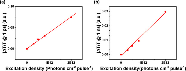
Finally, the observed effect can be a combination of the decay of the mobile electron concentration and the variation of μe(t). To examine a possible contribution of μe(t), we first assume that the electron concentration decay is independent of the excitation density, and the concentration is proportional to the excitation density at any delay times. Then, the observed slowing down of Δσ(t) should be associated with the increase in μe(t) as the charge concentration decreases. Contrary to this expectation, we observed that Δσ(t) increases linearly with the excitation density, both at early (see Figure 5a) and late (see Figure 5b) delays. These observations suggest a constant μe(t) over the presented range of excitations, which largely covers the density range used when slowing down of Δσ(t) was observed; see Figure 4a. We note here that at even higher excitations, Δσ(t) does not change linearly with the excitation density at early and late delay times; see Figure S5. The slope of the dependency of Δσ(t) on carrier concentration actually increases with time by ∼30%; see the Supporting information. Such an increase in μe(t) with time, which is excitation-independent at each delay, seems unreasonable. This implies that the observed Δσ(t) behavior is most probably related to the electron concentration decay function that changes with time, as discussed earlier. It is possible that μe(t) does contribute to the Δσ(t) decay changes as well, but it appears reasonable to assign most of the decay to the mobile electron dynamics.
Figure 5.
Photoconductivity of GaAs with 10 min nitridation measured at a delay time of (a) ∼1 ps and (b) ∼1 ns after photoexcitation at 1.6 eV under varied excitation fluencies.
It is noteworthy to consider the influence of the GaAs surface modification on the effect of charge diffusion, which should also reduce the concentration of mobile electrons and may increase their mobility, μe. We note here that surface modification should not affect the bulk of GaAs. Spatial distribution of photogenerated charge and thus their diffusion should not depend on the excitation density (within the linear excitation conditions) and on the status of the surface. Therefore, an identical effect of diffusion is expected for all GaAs samples independent of the surface treatment in a clear disagreement with the experimental observations; see Figure 4b.
Thus, we conclude that the dynamics of charge concentration is mainly responsible for the observed retardation of Δσ(t) decay with excitation density.
Further, we have compared TRPL and THz kinetics of GaAs with modified surfaces at similar excitation fluencies, as shown in Figure 6. We find that PL decays much faster than photoconductivity in GaAs with both the naturally oxidized and nitrided surfaces (∼140 and ∼400 ps vs ∼420 and ∼1310 ps, respectively). As discussed above, photoconductivity decay is at least partially associated with the mobile electron trapping, while PL decay depends on both electron and hole trapping. Much faster PL decay implies that PL dynamics is dominated by the hole-trapping process.
Figure 6.
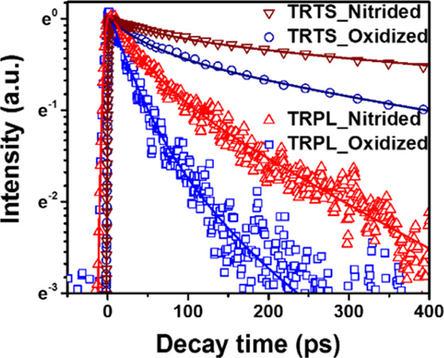
Normalized photoconductivity and PL kinetics of naturally oxidized GaAs and GaAs with 10 min nitridation after photoexcitation at 1.6 eV. The excitation photon flux in TRPL was 7 × 10¹² photons × cm–2 × pulse–1, and in TRTS, it was 2 × 10¹² photons × cm–2 × pulse–1. Solid lines are the fitting curves based on double-exponential functions. Fitted parameters are shown in the Supporting Information.
Based on the comparison of PL and photoconductivity decays, we also suggest to reconsider the applicability of the frequently used terminology of surface recombination velocity (SRV). According to the definition of SRV, charges generated in materials move to the material’s surface where they instantly recombine either with each other or with trapped charges. From our data, it is obvious that PL decay is not dominated by charge recombination. Moreover, because the mobility of electrons is much faster than that of holes, SRV extracted from optical measurements was in general thought to be dominated by electron trapping. However, in this study, we find that the disappearance of mobile holes is faster than that of electrons. This observation indicates that the process on the surface should be reinterpreted. It appears that charge trapping rather than recombination can be extracted from PL dynamics; thus, “SRV” should be better renamed as “surface trapping velocity”.
At ambient conditions, a semiconductor surface is usually oxidized. To evaluate the stability of the modified GaAs surfaces, we measured PL decay after varying time of the GaAs exposure to air and to N2. In GaAs with a deoxidized surface, PL lifetime decreases by a factor of 2 after exposing it to air for 80 h, and the stabilized PL lifetime is nearly identical to that of the naturally oxidized GaAs, as shown in Figure 7. In contrast, within 60 h of N2 exposure, we did not observe any pronounced change in the PL lifetime in the deoxidized GaAs. These observations suggest an unexpected conclusion that the GaAs surface deoxidized by HCl is resistant to air exposure. The measured time contradicts the traditional belief that surface oxidation occurs nearly instantly.52,53 The slower oxidation time should be related to the replacement of chlorine on the surface of GaAs with oxygen, which apparently takes time. After surface nitridation, we did not observe any measurable change in the PL lifetime during 80 h exposure to air. Apparently, surface nitridation results in resistive passivation of the GaAs surface, which could be of significant importance for multiple applications of GaAs crystals.
Figure 7.
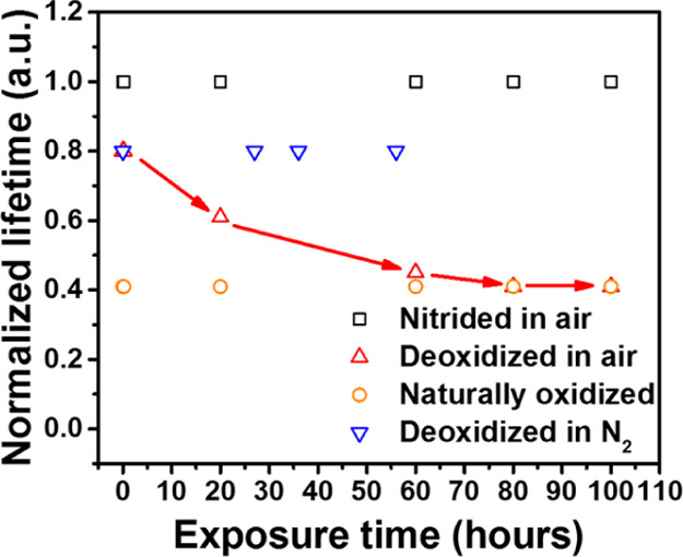
PL lifetime of deoxidized, naturally oxidized, and nitrided GaAs as a function of exposure time in air or nitrogen.
Conclusions
In summary, we have investigated the effect of wet passivation in GaAs wafers by nitridation in a low-alkaline hydrazine sulfide solution. Recombination processes of photogenerated carriers are studied in naturally oxidized, deoxidized, and nitrided intrinsic GaAs wafers by means of time-resolved and steady-state spectroscopy. We found that the trap-assisted nonradiative recombination dominates the overall recombination process. The decay of photoconductivity is much slower than the PL decay, indicating that the hole-trapping process dominates PL quenching in GaAs (100). After optimized nitridation of GaAs (100), hole and electron-trapping rates reduce compared to naturally oxidized GaAs by factors of 2.6 and 3, respectively. Unpassivated deoxidized GaAs (100) exposed to air undergoes oxidation in tens of hours. On the contrary, nitrided GaAs (100) is resistive to air over at least 100 h. This study not only demonstrates efficient chemical and electronic passivation by nitridation but also dwells on the details of the carrier recombination processes on the surface of GaAs (100).
Acknowledgments
X.Z. thanks Prof. Ebbe Nordlander in Chemical Physics, Lund University, for the assistance and help in the wet passivation experiment. This work is supported by the China Scholarship Council (201608440294, 201607040037, 201508340059, and 201506360083), the Natural Science Foundation of Guangdong Province (2019A1515010783), the Guangzhou Science and Technology Plan Project (202001010002), the Young Talents Program of Guangzhou University (RQ2020080), NanoLund in Lund University (p22-2015; p18-2017), the Swedish Research Council (2014-05490), the Swedish Energy Agency (34132-1),the Knut and Alice Wallenberg Foundation (KAW 2013.0284), and the Crafoord Foundation (20160772). D.F.S. acknowledges support from the European Union through the Marie Sklodowska-Curie Grant Agreement (590 702694).
Supporting Information Available
The Supporting Information is available free of charge at https://pubs.acs.org/doi/10.1021/acsami.0c04892.
Experimental details; PL emissions and absolute PLQY of naturally oxidized, deoxidized, and nitrided GaAs samples; TRPL and TRTS kinetics of naturally oxidized and deoxidized GaAs under varied excitation fluence; photoconductivity of naturally oxidized, deoxidized, and nitrided GaAs samples at varied excitation fluence; fitting parameters in Figures 3c, 4b, and 6 (PDF).
The authors declare no competing financial interest.
Supplementary Material
References
- Schnitzer I.; Yablonovitch E.; Caneau C.; Gmitter T. J. Ultrahigh Spontaneous Emission Quantum Efficiency, 99.7% Internally and 72% Externally, from AlGaAs/GaAs/AlGaAs Double Heterostructures. Appl. Phys. Lett. 1993, 62, 131–133. 10.1063/1.109348. [DOI] [Google Scholar]
- Warner J. H.; Walters R. J.; Messenger S. R.; Summers G. P.; Khanna S. M.; Estan D.; Erhardt L. S.; Houdayer A. High-Energy Proton Irradiation Effects in GaAs Devices. IEEE Trans. Nucl. Sci. 2004, 51, 2887–2895. 10.1109/tns.2004.835071. [DOI] [Google Scholar]
- Zdoroveyshchev A. V.; Zvonkov B. N.; Malysheva E. I.; Yakovlev G. E.; Zubkov V. I.; Dudin A. L.; Kudrin A. V.; Danilov Y. A.; Dorokhin M. V. Specific Features of the Electrochemical Capacitance–Voltage Profiling of GaAs LED and pHEMT Structures with Quantum-Confined Regions. Semiconductors 2018, 52, 1004–1011. 10.1134/s1063782618080250. [DOI] [Google Scholar]
- Jiang H.; Liu C. Y.; Qu Y.; Yuan S.; Liu G.; Bo B. High-Power InAlGaAs/GaAs and AlGaAs/GaAs Semiconductor Laser Arrays Emitting at 808 nm. IEEE Photon. Technol. Lett. 2004, 16, 389–391. 10.1109/lpt.2003.822247. [DOI] [Google Scholar]
- Hudait M. K.; Krupanidhi S. B. Effects of Thin Oxide in Metal-Semiconductor and Metal-Insulator-Semiconductor Epi-GaAs Schottky Diodes. Solid. State. Electron. 2000, 44, 1089–1097. 10.1016/s0038-1101(99)00320-2. [DOI] [Google Scholar]
- Wang X.; Dong L.; Zhang J.; Liu Y.; Ye P. D.; Gordon R. G. Heteroepitaxy of La2O3 and La2-xYxO3 on GaAs (111)A by Atomic Layer Deposition: Achieving Low Interface Trap Density. Nano Lett. 2013, 13, 594–599. 10.1021/nl3041349. [DOI] [PubMed] [Google Scholar]
- Kirchner C.; George M.; Stein B.; Parak W. J.; Gaub H. E.; Seitz M. Corrosion Protection and Long-Term Chemical Functionalization of Gallium Arsenide in an Aqueous Environment. Adv. Funct. Mater. 2002, 12, 266–276. . [DOI] [Google Scholar]
- Lee H. H.; Racicot R. J.; Lee S. H. Surface Passivation of GaAs. Appl. Phys. Lett. 1989, 54, 724–726. 10.1063/1.100873. [DOI] [Google Scholar]
- Szuber J.; Hollinger G.; Bergignat E. Sulfide Passivation of GaAs Surface. Electron. Technol. 1998, 31, 328–337. [Google Scholar]
- Terada Y.; Shimogaki Y.; Nakano Y.; Sugiyama M. In Situ Anti-Oxidation Treatment in GaAs MOVPE by as Desorption and Passivation with AlP. J. Cryst. Growth 2010, 312, 1359–1363. 10.1016/j.jcrysgro.2009.11.065. [DOI] [Google Scholar]
- Pankove J. I.; Berkeyheiser J. E.; Kilpatrick S. J.; Magee C. W. Passivation of GaAs Surfaces. J. Electron. Mater. 1983, 12, 359–370. 10.1007/bf02651137. [DOI] [Google Scholar]
- Anantathanasarn S.; Ootomo S.-y.; Hashizume T.; Hasegawa H. Surface Passivation of GaAs by Ultra-Thin Cubic GaN Layer. Appl. Surf. Sci. 2000, 159–160, 456–461. 10.1016/s0169-4332(00)00077-5. [DOI] [Google Scholar]
- Aierken A.; Riikonen J.; Mattila M.; Hakkarainen T.; Sopanen M.; Lipsanen H. GaAs Surface Passivation by Ultra-Thin Epitaxial GaP Layer and Surface As-P Exchange. Appl. Surf. Sci. 2007, 253, 6232–6235. 10.1016/j.apsusc.2007.01.069. [DOI] [Google Scholar]
- Riikonen J.; Sormunen J.; Koskenvaara H.; Mattila M.; Sopanen M.; Lipsanen H. Passivation of GaAs Surface by Ultrathin Epitaxial GaN Layer. J. Cryst. Growth 2004, 272, 621–626. 10.1016/j.jcrysgro.2004.08.110. [DOI] [Google Scholar]
- Kumar N. M.; Chikhalkar A.; King R. R. Effect of Deposited Passivation Materials and Doping on Recombination at III-V Surfaces. Conf. Rec. IEEE Photovolt. Spec. Conf. 2019, 1039–1043. 10.1109/pvsc40753.2019.8980913. [DOI] [Google Scholar]
- Anantathanasarn S.; Hasegawa H. Photoluminescence and Capacitance–voltage Characterization of GaAs Surface Passivated by an Ultrathin GaN Interface Control Layer. Appl. Surf. Sci. 2002, 190, 343–347. 10.1016/s0169-4332(01)00840-6. [DOI] [Google Scholar]
- Arab S.; Chi C.-Y.; Shi T.; Wang Y.; Dapkus D. P.; Jackson H. E.; Smith L. M.; Cronin S. B. Effects of Surface Passivation on Twin-Free GaAs Nanosheets. ACS Nano 2015, 9, 1336–1340. 10.1021/nn505227q. [DOI] [PubMed] [Google Scholar]
- Hocevar M.; Thanh Giang L. T.; Songmuang R.; Den Hertog M.; Besombes L.; Bleuse J.; Niquet Y. M.; Pelekanos N. T. Residual Strain and Piezoelectric Effects in Passivated GaAs/AlGaAs Core-Shell Nanowires. Appl. Phys. Lett. 2013, 102, 191103. 10.1063/1.4803685. [DOI] [Google Scholar]
- Andreev V. M.; Kazantsev A. B.; Khvostikov V. P.; Paleeva E. V.; Rumyantsev V. D.; Shvarts M. Z.. High-Efficiency (24.6% AM 0) LPE Grown AlGaAs/GaAs Concentrator Solar Cells and Modules. Proceedings of 1994 IEEE 1st World Conference on Photovoltaic Energy Conversion - WCPEC (A Joint Conference of PVSC, PVSEC and PSEC); IEEE, 1994, 2, 2096–2099.
- Fujieda S.; Mizuta M.; Matsumoto Y. Improvement of the Electrical Properties of the AlN/GaAs MIS System and Their Thermal Stability by GaAs Surface Stoichiometry Control. Jpn. J. Appl. Phys. 1988, 27, 296–299. 10.1143/jjap.27.l296. [DOI] [Google Scholar]
- Meiners L. G.; Wieder H. H. Semiconductor Surface Passivation. Mater. Sci. Rep. 1988, 3, 139–216. 10.1016/s0920-2307(88)80008-2. [DOI] [Google Scholar]
- Bessolov V. N. Passivation of GaAs in Alcohol Solutions of Ammonium Sulfide. Semiconductors 1997, 31, 1164. 10.1134/1.1187289. [DOI] [Google Scholar]
- Berkovits V. L.; Ulin V. P.; Losurdo M.; Capezzuto P.; Bruno G. Wet Chemical Treatment in Hydrazine-Sulfide Solutions for Sulfide and Nitride Monomolecular Surface Films on GaAs(100). J. Electrochem. Soc. 2005, 152, 349–353. 10.1149/1.1878032. [DOI] [Google Scholar]
- Dmitruk N. L.; Borkovskaya O. Y.; Mamontova I. B. Sulfide Passivation of a Textured Interface of a Gallium Arsenide Surface-Barrier Photovoltaic Cell. Tech. Phys. 2002, 44, 726–728. 10.1134/1.1259454. [DOI] [Google Scholar]
- Lunt S. R.; Ryba G. N.; Santangelo P. G.; Lewis N. S. Chemical Studies of the Passivation of GaAs Surface Recombination Using Sulfides and Thiols. J. Appl. Phys. 1991, 70, 7449–7467. 10.1063/1.349741. [DOI] [Google Scholar]
- Berkovits V. L.; Ulin V. P.; Losurdo M.; Capezzuto P.; Bruno G.; Perna G.; Capozzi V. Wet Chemical Nitridation of GaAs (100) by Hydrazine Solution for Surface Passivation. Appl. Phys. Lett. 2002, 80, 3739–3741. 10.1063/1.1479212. [DOI] [Google Scholar]
- Alekseev P. A.; Dunaevskiy M. S.; Ulin V. P.; Lvova T. V.; Filatov D. O.; Nezhdanov A. V.; Mashin A. I.; Berkovits V. L. Nitride Surface Passivation of GaAs Nanowires: Impact on Surface State Density. Nano Lett. 2015, 15, 63–68. 10.1021/nl502909k. [DOI] [PubMed] [Google Scholar]
- Berkovits V. L.; Ulin V. P.; Tereshchenko O. E.; Paget D.; Rowe A. C. H.; Chiaradia P.; Doyle B. P.; Nannarone S. GaAs(111)A and B in Hydrazine Sulfide Solutions: Extreme Polarity Dependence of Surface Adsorption Processes. Phys. Rev. B: Condens. Matter Mater. Phys. 2009, 80, 6–9. 10.1103/physrevb.80.233303. [DOI] [Google Scholar]
- An R.; Zhang F.; Zou X.; Tang Y.; Liang M.; Oshchapovskyy I.; Liu Y.; Honarfar A.; Zhong Y.; Li C.; Geng H.; Chen J.; Canton S. E.; Pullerits T.; Zheng K. Photostability and Photodegradation Processes in Colloidal CsPbI3 Perovskite Quantum Dots. ACS Appl. Mater. Interfaces 2018, 10, 39222–39227. 10.1021/acsami.8b14480. [DOI] [PubMed] [Google Scholar]
- Xu X.; Li Z.; Zhang W.; Meng X.; Zou X.; Di Carlo Rasi D.; Ma W.; Yartsev A.; Andersson M. R.; Janssen R. A. J.; Wang E. 8.0% Efficient All-Polymer Solar Cells with High Photovoltage of 1.1 V and Internal Quantum Efficiency near Unity. Adv. Energy Mater. 2018, 8, 1700908. 10.1002/aenm.201700908. [DOI] [Google Scholar]
- Rau U. Reciprocity Relation between Photovoltaic Quantum Efficiency and Electroluminescent Emission of Solar Cells. Phys. Rev. B: Condens. Matter Mater. Phys. 2007, 76, 85303. 10.1103/physrevb.76.085303. [DOI] [Google Scholar]
- Green M. Radiative Efficiency of State-of-the-art Photovoltaic Cells. Prog. Photovoltaics Res. Appl. 2012, 20, 472–476. 10.1002/pip.1147. [DOI] [Google Scholar]
- Thomas C.; Tamura Y.; Syazwan M. E.; Higo A.; Samukawa S. Oxidation States of GaAs Surface and Their Effects on Neutral Beam Etching during Nanopillar Fabrication. J. Phys. D Appl. Phys. 2014, 47, 215203. 10.1088/0022-3727/47/21/215203. [DOI] [Google Scholar]
- Surdu-Bob C. C.; Saied S. O.; Sullivan J. L. An X-Ray Photoelectron Spectroscopy Study of the Oxides of GaAs. Appl. Surf. Sci. 2001, 183, 126–136. 10.1016/s0169-4332(01)00583-9. [DOI] [Google Scholar]
- Berkovits V. L.; L’vova T. V.; Ulin V. P. Chemical Nitridation of GaAs(100) by Hydrazine-Sulfide Water Solutions. Vacuum 2000, 57, 201–207. 10.1016/s0042-207x(00)00126-3. [DOI] [Google Scholar]
- Berkovits V. L.; Ulin V. P.; Paget D.; Bonnet J. E.; L’vova T. V.; Chiaradia P.; Lantratov V. M. Chemical and Photochemical Processes in Sulfide Passivation of GaAs(100): In Situ Optical Study and Photoemission Analysis. J. Vac. Sci. Technol., A 1998, 16, 2528–2538. 10.1116/1.581377. [DOI] [Google Scholar]
- Tan C.-K.; Zhang J.; Li X.-H.; Liu G.; Tayo B. O.; Tansu N. First-Principle Electronic Properties of Dilute-as GaNAs Alloy for Visible Light Emitters. J. Disp. Technol. 2013, 9, 272–279. 10.1109/jdt.2013.2248342. [DOI] [Google Scholar]
- Lebedev M. V.; Mankel E.; Mayer T.; Jaegermann W. Wet Etching of GaAs(100) in Acidic and Basic Solutions: A Synchrotron-Photoemission Spectroscopy Study. J. Phys. Chem. C 2008, 112, 18510–18515. 10.1021/jp805568t. [DOI] [Google Scholar]
- Osakabe S.; Adachi S. Study of GaAs(001) Surfaces Treated in Aqueous HCl Solutions. Jpn. J. Appl. Phys. 1997, 36, 7119–7125. 10.1143/jjap.36.7119. [DOI] [Google Scholar]
- Zhang W.; Lehmann S.; Mergenthaler K.; Wallentin J.; Borgström M. T.; Pistol M.-E.; Yartsev A. Carrier Recombination Dynamics in Sulfur-Doped InP Nanowires. Nano Lett. 2015, 15, 7238–7244. 10.1021/acs.nanolett.5b02022. [DOI] [PubMed] [Google Scholar]
- Zhang W.; Zeng X.; Su X.; Zou X.; Mante P.-A.; Borgström M. T.; Yartsev A. Carrier Recombination Processes in Gallium Indium Phosphide Nanowires. Nano Lett. 2017, 17, 4248–4254. 10.1021/acs.nanolett.7b01159. [DOI] [PubMed] [Google Scholar]
- Yong C. K.; Wong-Leung J.; Joyce H. J.; Lloyd-Hughes J.; Gao Q.; Tan H. H.; Jagadish C.; Johnston M. B.; Herz L. M. Direct Observation of Charge-Carrier Heating at WZ–ZB InP Nanowire Heterojunctions. Nano Lett. 2013, 13, 4280. 10.1021/nl402050q. [DOI] [PubMed] [Google Scholar]
- Yablonovitch E.; Skromme B. J.; Bhat R.; Harbison J. P.; Gmitter T. J. Band Bending, Fermi Level Pinning, and Surface Fixed Charge on Chemically Prepared GaAs Surfaces. Appl. Phys. Lett. 1989, 54, 555–557. 10.1063/1.100929. [DOI] [Google Scholar]
- Reddy P.; Bryan I.; Bryan Z.; Guo W.; Hussey L.; Collazo R.; Sitar Z. The Effect of Polarity and Surface States on the Fermi Level at III-Nitride Surfaces. J. Appl. Phys. 2014, 116, 123701. 10.1063/1.4896377. [DOI] [Google Scholar]
- Su X.; Zeng X.; Němec H.; Zou X.; Zhang W.; Borgström M. T.; Yartsev A. Effect of Hydrogen Chloride Etching on Carrier Recombination Processes of Indium Phosphide Nanowires. Nanoscale 2019, 11, 18550–18558. 10.1039/c9nr03187a. [DOI] [PubMed] [Google Scholar]
- Rode D. L. Chapter 1 Low-Field Electron Transport.. Semiconduct. Semimet. 1975, 10, 1–89. 10.1016/s0080-8784(08)60331-2. [DOI] [Google Scholar]
- Wiley J. D. Chapter 2 Mobility of Holes in III-V Compounds.. Semiconduct. Semimet. 1975, 10, 91–174. 10.1016/s0080-8784(08)60332-4. [DOI] [Google Scholar]
- Boland J. L.; Casadei A.; Tütüncüoglu G.; Matteini F.; Davies C. L.; Jabeen F.; Joyce H. J.; Herz L. M.; Fontcuberta i Morral A.; Johnston M. B. Increased Photoconductivity Lifetime in GaAs Nanowires by Controlled N-Type and P-Type Doping. ACS Nano 2016, 10, 4219–4227. 10.1021/acsnano.5b07579. [DOI] [PubMed] [Google Scholar]
- Wolfe C. M.; Stillman G. E.; Lindley W. T. Electron Mobility in High-Purity GaAs. J. Appl. Phys. 1970, 41, 3088–3091. 10.1063/1.1659368. [DOI] [Google Scholar]
- Sotoodeh M.; Khalid A. H.; Rezazadeh A. A. Empirical Low-Field Mobility Model for III-V Compounds Applicable in Device Simulation Codes. J. Appl. Phys. 2000, 87, 2890–2900. 10.1063/1.372274. [DOI] [Google Scholar]
- Blakemore J. S. Semiconducting and Other Major Properties of Gallium Arsenide. J. Appl. Phys. 1982, 53, R123–R181. 10.1063/1.331665. [DOI] [Google Scholar]
- DeSalvo G. C. Wet Chemical Digital Etching of GaAs at Room Temperature. J. Electrochem. Soc. 1996, 143, 3652. 10.1149/1.1837266. [DOI] [Google Scholar]
- Lukeš F. Oxidation of Si and GaAs in Air at Room Temperature. Surf. Sci. 1972, 30, 91–100. 10.1016/0039-6028(72)90025-8. [DOI] [Google Scholar]
Associated Data
This section collects any data citations, data availability statements, or supplementary materials included in this article.


