Abstract
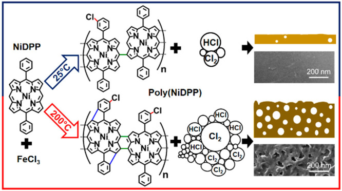
Porous and highly conjugated multiply fused porphyrin thin films are prepared from a fast and single-step chemical vapor deposition approach. While the solution-based coupling of porphyrins is usually undertaken at room temperature, the gas phase reaction of nickel(II) 5,15-(diphenyl)porphyrin and iron(III) chloride (FeCl3) is investigated for temperatures as high as 200 °C. Helium ion and atomic force microscopy, supported by weight and thickness measurements, shows a drastic decrease of the fused porphyrin thin film’s density accompanied by the formation of a mesoporous morphology upon increase of the reaction temperature. The increase of the film’s porosity is attributed to formation of a greater amount of HCl (originated from both the oxidative coupling and chlorination reactions) and the release of gaseous FeCl3 byproducts, i.e., Cl2, at higher deposition temperatures. In addition, high resolution mass spectrometry reveals that increase of the reaction temperature promotes a higher degree of conjugation of the fused porphyrins chains, which ensures that high electronic conductivities are maintained along with high porosity. The method reported herein could enable the engineering of fused porphyrin thin films in sensing and catalytic devices.
Keywords: fused porphyrins, conjugated polymers, oxidative coupling, thin films, chemical vapor deposition
Introduction
Porphyrins, composed of four pyrrole subunits connected by methine bridges, possess numerous fascinating properties, including a strong aromaticity responsible for attractive absorption or emission properties and a rich metal coordination chemistry that have made them the catalysts of choice in the main processes allowing life (photosynthesis and respiration). Several studies have reported the cooperative effect promoted by conjugated covalent links between porphyrins. Particularly, conjugated porphyrin arrays or polymers own superior functional properties, such as an increased catalytic activity.1−3 Among the conjugated porphyrin systems, directly fused porphyrin tapes possess even more fascinating properties with a NIR absorption,4 two-photon absorption,5 and negative attenuation factors.6,7
Up to recently, the synthesis of fused porphyrin tapes involved the solution-based dehydrogenative coupling of porphyrins using adequate oxidants. Nevertheless, the very poor solubility of these compounds limits the potential substituents to bulky solubilizing groups and prevents their integration into functional devices. Several studies have also reported the formation of fused porphyrin tapes from the sublimation under ultrahigh vacuum onto oriented metal surfaces.8,9 However, the latter approach is solely yielding the formation of submonolayers and is completely dependent on the underlying substrate, preventing the fabrication of functional devices. To circumvent the poor solubility of fused porphyrin tapes, we very recently developed a chemical vapor deposition (CVD) method toward the simultaneous synthesis, deposition, and doping of fused porphyrin thin films.10,11 In this method, the porphyrin and the oxidant are both delivered through the vapor phase onto a substrate on which they adsorb and react to form multiply fused porphyrin tapes. While solution-based approaches produce fused porphyrin oligomers in moderate yields even with the aid of bulky substituents to suppress undesired aggregation,4,12,13 the oxidative chemical vapor deposition (oCVD) reaction of porphyrins ensures excellent yields of polymerization. The effective polymerization is expressed by the electrical conductivity of the thin films that reaches up to 1 S cm–1 and a strong absorption in the visible to near-infrared spectral region.
Nevertheless, the advantages related to the oCVD of porphyrins go far beyond its unique ability to form fused porphyrin thin films. Indeed, processing through the gas phase allows to circumvent the limitation related to the poor solubility of fused porphyrins and to decouple the porphyrin substituents from the synthesis requirements. This enable the use of smaller substituents, i.e., phenyl, that ensures the formation of dense and homogeneous thin films with superior conductivity.14 In addition, the higher reactivity of the porphyrins in oCVD enables the synthesis of fused porphyrins chelating different metal cations, i.e., Co(II), Ni(II), Cu(II), Zn(II), and Pd(II).15 In this work, we further take advantage of this new synthesis approach to investigate the dehydrogenative coupling of nickel(II) porphyrins at different temperatures. Indeed, while the solution-based coupling of porphyrins is usually undertaken at room temperature and cannot be performed at significantly higher temperature due to the use of organic solvent, oCVD allowed the study of the dehydrogenative coupling of porphyrins at temperature as high as 200 °C. Ultraviolet–visible–near-infrared (UV/vis/NIR) spectroscopy, laser desorption ionization high resolution mass spectrometry (LDI-HRMS), and X-ray photoelectron spectroscopy (XPS) allowed to elucidate the influence of the substrate temperature on the chemistry of the fused porphyrin thin films. Moreover, previous studies on the oCVD reaction of 3,4-ethylenedioxythiophene (EDOT) have shown that modulating the reaction (substrate) temperature allowed to tune the porosity and pore size of poly(3,4-ethylenedioxythiophene) (PEDOT) thin films.16 Therefore, in the present work we investigate the ability of oCVD for the growth of porous fused porphyrin thin films. The impact of the substrate temperature on the growth rate, morphology, and nanomechanical properties is investigated by means of helium ion microscopy (HIM), atomic force microscopy (AFM), and water uptake measurements.
Experimental Section
Oxidative Chemical Vapor Deposition
The oCVD experiments described in this paper were performed in a custom-built oCVD reactor described elsewhere (Scheme S1).10,11 In this study, the porphyrin and oxidant evaporators were loaded with 10 mg of nickel(II) 5,15-(diphenyl)porphyrin (NiDPP) and ∼150 mg of iron(III) chloride (FeCl3). Porphyrin’s and oxidant’s evaporator temperatures were kept at 250 and 150 °C, respectively, when substrate holder’s temperature was varied from room temperature to 200 °C (Table S1). The deposition chamber was maintained at a pressure of 10–3 mbar under an argon atmosphere, and the deposition time was set to 30 min for all experiments. Microscope glass slides (Menzel-Gläser, 76 × 26 mm2), silicon wafers, and organic field effect transistor chips (OFET) (Fraunhofer) were used as substrates. NiDPP and FeCl3 monomers were obtained from PorphyChem (98%) and Sigma-Aldrich (97%), respectively, and used without further purification.
Thin Film Characterizations
The electrical conductivity was measured by depositing the films onto commercial OFET chips. The measurements were done without applying any gate voltage and by recording the current–voltage scans with a two-point probe to extract the conductivity by using Ohm’s law. The thickness of the films was measured by using an Alpha step d-500 profilometer from KLA-Tencor. The surface density was assessed from the specific mass gain due to the deposition and the area of the coated surface: surface density [μg cm–2] = (m1 – m0)/A, where m0 and m1 are the masses of the coated and uncoated substrate, respectively, while A is the coated area estimated by using ImageJ software. Coated microscope glass slides were weighted by using a microbalance (Sartorius ME36S) to obtain m1, and then the samples were immersed in a mixture of acetone/ethanol (50:50%) for 2 min before being cleaned with Kimtech tissues to remove all the deposited film and obtain m0. The surface density measurement was repeated on three different samples for each deposition condition to determine the average surface density. The film’s density (g cm–3) was calculated from the measured surface density and the thickness of each film. The static water contact angles (WCA) were evaluated from five different measurements undertaken at different position for each sample by using a contact angle measuring instrument (KRÜSS EasyDrop). The water uptake of the films was evaluated on coated glass substrates by measuring the mass difference of the totally hydrated (mwet) and vacuum-dried films (mdry). Initially, the water from the fully hydrated films was carefully blotted with Kimtech tissues then dried in a vacuum oven at 70 °C for 24 h. The water uptake measurement was repeated five times for each of the prepared thin films, and the average value and standard deviation of these measurements are reported.
The optical absorbance was measured in the range 250–2500 nm by using an UV/vis/NIR spectrophotometer (PerkinElmer, Lambda 950) with a 150 mm diameter integrating sphere. The absorbance of the as-deposited and acetone rinsed films was measured on the glass substrates. The absorbance of the acetone-soluble phase of the films was measured in quartz cuvettes of 3.5 mL and 1 cm light path. The helium ion microscope (HIM) images were recorded with an Orion Nanofab Instrument from Zeiss. The images were acquired from thin film samples deposited on silicon wafers. Helium ions are generated using a gas field ionization source (GFIS). Within the GFIS a sharp needle having an apex radius of ∼100 nm is set to a positive high voltage with respect to an extraction electrode. Ionization of helium atoms happens in close proximity of the sharp needle, and a helium ion beam is extracted through an opening in the extraction electrode. An impact energy of 30 keV was used (energy of impinging ion beam at sample location), with ion current between 0.1 and 1 pA and a tilt angle of the substrate holder stage of 20°. The helium ion beam scans the sample surface creating secondary electrons (SE). The contrast in the images is created mainly by material composition and topography. Compared to the standard secondary electron microscope (SEM), the HIM allows to probe specimens with a better surface sensitivity and a higher depth of field which makes it very suitable for topographic imaging.17 Quantitative images of the topography and nanomechanical properties of the samples were acquired by using the AM-FM mode of the MFP-3D Infinity atomic force microscope (AFM) (Asylum Research). All measurements were made under ambient conditions (room temperature and relative humidity of about 50%), and a standard cantilever holder for operation in air was used. Images of a 2 × 2 μm2 area were taken with a resolution of 256 × 256 pixels at a scan rate of 3 Hz. Cantilevers’ spring constants used in this study were about 20–30 N m–1 (Olympus, AC160TS-R3). The first and second resonant frequencies for AC160TS-R3 cantilevers were about 238 kHz and 1.34 MHz, respectively. A relative calibration method was done to estimate the tip radius by using a dedicated reference samples kit provided by Bruker (PFQNM-SMPKIT-12m). The deflection sensitivity and the spring constant of the cantilever were determined by using the GetReal Automated Probe Calibration feature. The tip radius was adjusted to obtain the proper value of 2.7 GPa for the polystyrene reference, matching the deformation applied on the sample of interest. To ensure repulsive intermittent contact mode, the amplitude set point was chosen as Aset point/A0 = ca. 0.7 so that the phase is well fixed at 60°. The reported average and standard deviation values of modulus and roughness (Ra) consider at least three images in each sample for reliable results.
Secondary ion mass spectrometry (SIMS) measurements were performed on a CAMECA NanoSIMS 50 using a Cs+ primary ion beam with an impact energy of 16 keV and a current of around 1.5 pA on sample surface. The masses studied simultaneously in multicollection mode were 12C14N, 35Cl, and 56Fe12O. Images were acquired at a size of 40 × 40 μm2 and 256 × 256 pixels. Secondary electron (SE) images were recorded by using the same SIMS instrument. Atmospheric-pressure laser desorption/ionization coupled with a high-resolution mass spectrometry (AP-LDI-HRMS) was used for the characterization and identification of the oligomers produced by the oCVD reaction of NiDPP with FeCl3. HRMS analyses were performed with an LTQ/Orbitrap Elite Hybrid Linear Ion Trap-Orbitrap mass spectrometer from Thermo Scientific (San Jose, CA) coupled with an AP-MALDI (ng) UHR source from MassTech Inc. (Columbia, MA) with a 355 nm Nd:YAG laser. The as-deposited NiDPP-based thin films were directly probed, without any matrix deposition, by the laser following a spiral motion during 30 s per sample. An in-source decay (ISD) of 70 V was applied to the samples to prevent any formation of noncovalent NiDPP clusters that could interfere with the distribution of the NiDPP oligomers. A maximum injection time of 800 ms and a resolving power of 240000 at m/z 400 within the normal mass range (m/z 300–2000) and the high mass range (m/z 1800–4000) were employed for the HRMS analyses. X-ray photoelectron spectroscopy (XPS) analyses were performed on a Kratos Axis Ultra DLD instrument using a monochromatic Al Kα X- ray source (Zυ = 1486.6 eV) at a power of 105 W. Charge calibration was accomplished by fixing the binding energy of carbon (C 1s) to 285.0 eV.
Results and Discussion
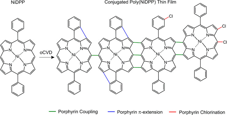
A series of fused porphyrin tapes thin films were prepared from the oCVD reaction of nickel(II) 5,15-(diphenyl)porphyrin (NiDPP) and iron(III) chloride (FeCl3) at different substrate temperatures. NiDPP was selected due to its proven ability to form multiply fused porphyrin tapes in oCVD,18 while FeCl3 was previously demonstrated as a better choice to promote the dehydrogenative coupling of porphyrins over their undesired chlorination11 (Scheme 1). Particularly, FeCl3 can oxidize a porphyrin core to yield a porphyrin radical cation, which can subsequently reacts with the meso-position of a neutral porphyrin to form an adduct stabilized through the elimination of H+ (Scheme S2).18 Porphyrin dimers and longer oligomers are formed concurrently to the release of FeCl2 and HCl as byproducts. Substrate temperature was varied from room temperature (25 °C), traditionally used in solution-based approaches,19 to 200 °C, which can only be investigated through the proposed gas phase method (Table S1).
Scheme 1. Illustration of the Reactions Occurring during the OCVD Reaction of NiDPP.
Alongside the targeted dehydrogenative coupling of NiDPP, which can form singly, doubly, or triply fused porphyrin tapes, chlorination and π-extension via ring fusion can occur.18
Irrespective of the substrate temperature, the oCVD reaction of NiDPP and FeCl3 yields the formation of macroscopically smooth and uniform thin films with an electrical conductivity in the range of 10–3–10–2 S cm–1 (Table S2). The oCVD thin films exhibit colorations that strongly differ from the light orange color of the reference thin films prepared from the sublimation of NiDPP without oxidant. Such a color change, already observed in previous studies, is indicative of the formation of fused porphyrin tapes.10 Nevertheless, the color gradient between the greenish coloration of the oCVD thin films elaborated at the lowest substrate temperatures and the dark brownish color of the oCVD thin films obtained for the highest substrate temperatures (Figure 1) hints at a difference in the deposition rate and/or in the reactivity, i.e., different reaction kinetics between the dehydrogenative coupling, chlorination, and π-extension via ring fusion of the porphyrins (Scheme 1).
Figure 1.
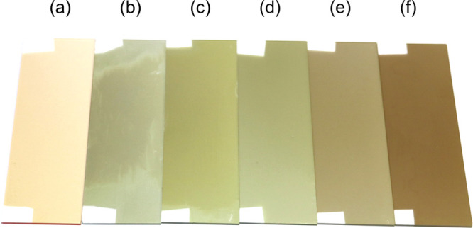
Photography of the thin films obtained from (a) the sublimation of NiDPP and (b–f) oCVD reaction of NIDPP and FeCl3 at different substrate temperatures: (b) 25, (c) 50, (d) 100, (e) 150, and (f) 200 °C. (a) Substrate temperature was 150 °C for the preparation of the reference thin film without oxidant.
Influence on the Morphology and Growth
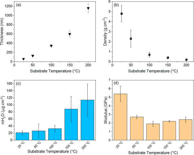
Contact profilometry measurements highlighted strong discrepancies between the thicknesses of the oCVD thin films. Indeed, increase of the substrate temperature from room temperature and 200 °C yields an increase of the oCVD thin films’ thickness from 60 nm to 1.2 μm (Figure 2a). Interestingly, irrespective of the substrate temperature, the thickness of the reference thin films deposited at 25–200 °C was shown constant at ca. 50 nm. In spite of the large growth rate discrepancies observed for the oCVD thin films, their weight per unit area was shown constant (ca. 27 μg cm–2) for all the investigated substrate temperatures, from ca. 29 μg cm–2 for the oCVD thin film formed at room temperature to ca. 26 μg cm–2 for the one deposited at 200 °C (Table S2). One should note that weight per unit area (ca. 28 μg cm–2) of the reference thin films is highly similar to the ones of the oCVD thin films. Such an observation is consistent with the identical amounts of NiDPP sublimed for the preparation of all the thin films reported in this work (Table S1) but suggests strong variations in the density of the films. Indeed, the calculated density is shown to drastically decrease with increase of the substrate temperature (Figure 2b). The densities calculated for the reference thin films (ca. 4.7 ± 2.4 g cm–3) and the oCVD thin film elaborated at 25 °C (ca. 4.8 ± 0.8 g cm–3) are over 20 times greater than the one calculated for the oCVD thin film elaborated at 200 °C (ca. 0.2 ± 0.1 g cm–3).
Figure 2.
(a) Measured thickness, (b) calculated density, (c) measured water uptake, and (d) measured Young modulus for the oCVD thin films.
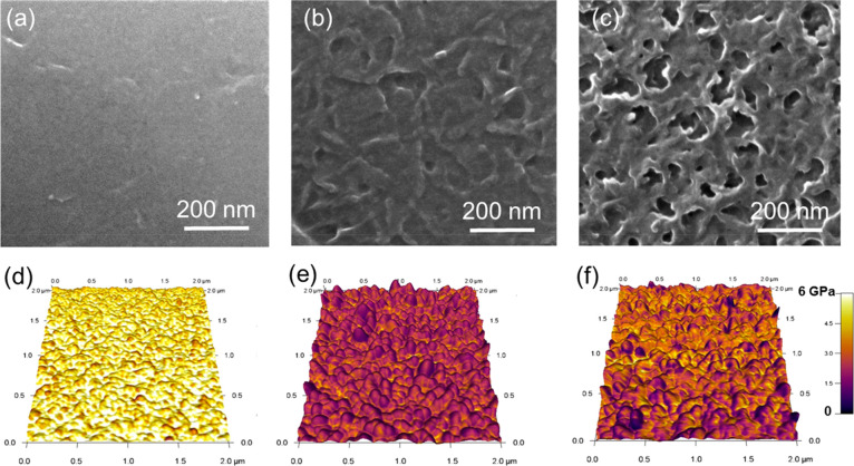
The variation of the film density (Figure 2b) correlates with the helium ion microscopy (HIM) analyses of the films that reveals different morphologies (Figure 3 and Figure S1). While the oCVD thin film prepared at room temperature shows a relatively dense and smooth surface (Figure 3a), the oCVD thin films prepared at higher substrate temperatures display rough and textured surface (Figure 3b,c). In particular, the oCVD thin film elaborated at 200 °C exhibit a mesoporous structure with numerous voids in the range 10–50 nm. Such an observation correlates with the report by Gleason et al. on the formation of nanoporous PEDOT films whose pores are induced by the outgassing of bubbles formed during the oCVD reaction.16 However, some discrepancies exist with our work where the high sticking coefficient of the porphyrin molecules, sublimed at 250 °C on a substrate maintained at a lower temperature (25 to 200 °C), implies that the porphyrins deposit and remain on the substrate surface even if nonpolymerized.20 Such a behavior is illustrated by the reference thin films prepared from the sole sublimation of NiDPP (Figure 1). This highlights the key roles of FeCl3 used in excess in the present work (Table S1) and the reaction temperature in the formation of highly porous fused porphyrin thin films in oCVD. We suggest that FeCl3 and the substrate temperature can affect the porosity of the films in two different ways: (i) increased reactivity at higher temperatures and (ii) decomposition of FeCl3 into gaseous products at higher temperatures. First, the enhanced reactivity at higher temperatures promotes the oxidative coupling (as suggested by the weak solubility of the film produced at 200 °C, Figure S2) and chlorination reactions that all yield the formation of a greater amount of HCl. The formation of HCl during the oCVD reaction of FeCl3 and porphyrins has previously been evidenced from the demetalation of zinc(II) 5,15-(dimesityl)porphyrin and the protonation of free-base 5,15-(dimesityl)porphyrin (H2DMP) to [H3DMP]+ and [H4DMP]2+.15 The fast condensation of the porphyrin units and fused porphyrin tapes is suggested to slow down the escape of gaseous HCl from the films, favoring the formation of porous structures. On the other hand, FeCl3 is known to decompose to FeCl2 and gaseous Cl2 upon heating.21,22 Thus, gaseous FeCl3 byproducts can bubble out from the film during oCVD process, further contributing to the expansion of the structure and formation of pores and holes.
Figure 3.
(a–c) Helium ion microscopy images and (d–f) mapping of the local Young modulus from the elastic deformations observed by atomic force microscopy of the oCVD thin films elaborated at a substrate temperature of (a, d) 25 °C, (b, e) 150 °C, and (c, f) 200 °C.
Dynamic secondary-ion mass spectrometry (D-SIMS) reveals hot spots of 35Cl and 56Fe16O fragments at the surface of all the oCVD thin films. In particular, clusters of 35Cl and 56Fe16O fragments are detected at the surface of the thin film elaborated at a substrate temperature of 200 °C (Figure 4), confirming that iron chloride can accumulate at the surface of the film even though brought at a temperature higher than the one used to sublime FeCl3 (150 °C) (Figures S3 and S4). Quantitatively, X-ray photoelectron spectroscopy (XPS) confirmed that, irrespective of the substrate temperature, highly similar amounts of iron (2.6 to 3.7 ± 1.0 at. %) and chlorine (2.0 to 2.5 ± 1.0 at. %) were present at the surface of the oCVD thin films (Table S3). Iron and chlorine elements can be present in different forms in the oCVD thin films. First, FeCl2 and HCl are both produced during the dehydrogenative coupling of porphyrins. If HCl is very likely desorbed, FeCl2 can remain in the films and later oxidizes spontaneously into iron(III) species upon exposure to air, creating residues of iron(III) linked to oxygen and chlorine atoms. In addition to the metal chloride, chlorine may also substitute hydrogen atoms of the porphyrin macrocycle or substituents such as depicted in Scheme 1 and previously evidenced by XPS.11 Chlorine may also be available as dopant anion in the films.23 Finally, part of the FeCl3 remains unreacted in the films. One should note that excess of FeCl3 and its oxidation byproducts can be removed through a rinsing step with methanol such as reported by Gleason et al.23
Figure 4.
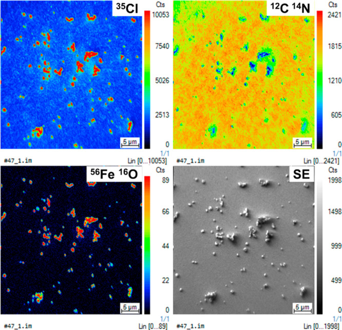
Elemental distribution of 12C14N, 35Cl, and 56Fe16O fragments originating from the porphyrin and oxidant and corresponding secondary electron image of the oCVD thin film prepared at a substrate temperature of 200 °C. The field of view is 40 × 40 μm2. Noticeably, the 35Cl hot spots match with the hot spots of the 56Fe16O fragments, which are both the exact negative of the 12C14N fragment.
The nanoscale morphology and mechanical properties of the oCVD thin films were imaged by atomic force microscopy (AFM) in the amplitude modulation–frequency modulation (AM–FM) mode. One can observe on the topography images the general trend of increasing roughness (Ra) of the films with substrate temperature (Figure S5), from Ra = 1.2 ± 0.4 nm for the film deposited at 25 °C to 6.7 ± 0.9 nm for the one deposited at 200 °C. The evolution of the Ra value, summarized in Table S2, correlates well with the thickness increase of the oCVD thin films upon increase of the substrate temperature. The Young’s modulus measurements, performed over three different areas of 2 × 2 μm2 for each sample (Figure 3d–f), reveal a decrease in the modulus values with the increase of substrate temperature (Figure 2d). Thanks to the calibration of the mechanical response of the AFM tip, the modulus value was evaluated to 5.4 ± 0.9 GPa for the oCVD thin film deposited at 25 °C to 2.4 ± 0.3 GPa for the film formed at 200 °C (Table S2). Interestingly, the decrease of the Young’s modulus can be related to the decrease of the film density (Figure 2b), both related to the formation of porosities during the oCVD reaction.
To confirm the evolution of the films porosity along with increase of the substrate temperature, water uptake measurements were undertaken. To ensure a fair comparison of the water uptake, the water contact angle (WCA) of the films was first measured. WCA varied from 69° to 89° for the as-deposited oCVD thin films and was shown to slightly increase to 87° to 105 °C for the oCVD thin films rinsed with water (Figure S6). Indeed, FeCl3 increases the polarity of the surface. Therefore, the solubilization and removal of FeCl3 (alongside its byproducts) by water causes an increase of the WCA (Figure S6). As shown in Figure 2c, an increase of the water uptake from 21 to 114 μg cm–2 is observed with increase of the substrate temperature. Increase of the water uptake is consistent with an increase of the porosity at higher substrate temperature. The ability to form porous fused porphyrin thin films and increase their specific surface area is particularly desirable for sensing or catalysis applications.24
Influence on the Oxidative Coupling and Chlorination
The UV/vis/NIR absorption spectra of the oCVD thin films (Figure 5) confirm the color change described above. Notably, the spectra reveal a progressive broadening of the Soret band (420 nm) and a red-shift and broadening of the Q bands (500–600 nm) upon increasing the substrate temperature. More importantly, all the oCVD thin films absorb up to the NIR region as much as 2500 nm such as expected for multiply fused porphyrin tapes, while singly fused porphyrins only exhibit absorption in the UV/vis region.25 In accordance with our previous reports,10,18 the oCVD thin films are almost insoluble in common organic solvents (Figure S2a–c). UV/vis/NIR analysis of the acetone-soluble phase ascertains the presence of unreacted FeCl3 for all the oCVD thin films and NiDPP monomer derivatives for the ones deposited at the lowest substrate temperatures (Figure S2c). Interestingly, NIR absorption is slightly more pronounced with the increase of the substrate temperatures (Figure 5b), suggesting a higher degree of conjugation for higher substrate temperatures.
Figure 5.
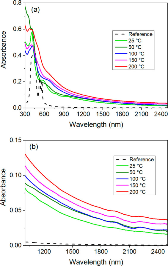
UV/vis/NIR absorption spectra of the reference and oCVD thin films in the ranges (a) 300–2500 nm and (b) 1000–2500 nm.
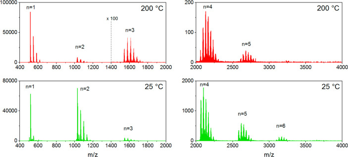
Atmospheric-pressure laser desorption/ionization high-resolution mass spectrometry (AP-LDI-HRMS) analysis confirms the successful oxidative polymerization of NiDPP irrespective of the substrate temperature. Up to hexameric oligomers are observed in the mass spectra (Figure 6 and Figure S7). In addition, AP-LDI-HRMS also evidences chlorination (+Cl–H)n and intramolecular cyclization (−H2)n reactions known to occur during the oCVD of porphyrins (Scheme 1).18 Although AP-LDI-HRMS analysis does not provide an exhaustive view into the mass distribution and that the intensities related to the different species detected are not fully related to their abundance, the high mass resolution (up to 240000 at m/z 400) and the high mass accuracy (around 3 ppm) of the technique enable the draw of informative trends.11 In particular, the analysis of the trimeric region of the spectra reveals a progressive shift of the maximum intensity toward lower masses (Figure S8). This is related to the increase in the number of unsaturation in the molecule (loss of 2H pairs) with the increase of the substrate temperature (Figure 7 and Figures S9 and S10). Indeed, when the substrate is held at 25 °C, the singly linked trimer [(NiDPP)3–H4]+ and the corresponding chlorinated compounds [(NiDPP)3–H4 (+Cl–H)n]+ are the dominant species detected among the trimers. On the contrary, highly unsaturated trimers [(NiDPP)3–H8]+ and the respective chlorinated trimers [(NiDPP)3–H8 (+Cl–H)n]+ become the preponderant species at 200 °C. This observations hint on the formation of mostly singly fused NiDPP trimers at low substrate temperatures to mostly doubly fused trimers at higher temperatures. For all cases, peaks related to the elimination of additional pairs of hydrogen atoms (−2H)n are detected, arising from (i) the intramolecular dehydrogenative cyclization between the phenyl rings and porphyrin macrocycles14 and (ii) the formation of triply fused oligomers.15 Indeed, Ni(II) diphenyl porphyrin can form double and triple linkages (Schemes S3 and S4) under oCVD conditions due to a mixing of the a1u and a2u radical characters that dictate the reaction’s regioselectivity.15 Particularly, the AP-LDI-HRMS spectrum of the oCVD thin film deposited at 200 °C shows the signal related to the formation of the triply fused porphyrin dimers with the four phenyl ring fused on the porphyrin core (m/zobserved = 1022.099, m/zcalculated = 1022.098; mass error <1 ppm) (Figure S11).
Figure 6.
AP-LDI-HRMS spectra of the oCVD thin films elaborated at 25 and 200 °C. Ions are detected as radical cations [M]•+. Two scan events were used to acquire spectra within a broad mass range (m/z 400–2000 and m/z 2000–4000).
Figure 7.
Relative abundance of the different trimeric species [(NiDPP)3–H2n (+Cl–H)m]+ detected by high-resolution mass spectrometry for the oCVD thin films deposited at 25, 100, and 200 °C. Such a presentation of the AP-LDI-HRMS data enables a better overview of the −2H pairs evolution, which cannot be readily observed from the AP-LDI-HRMS spectra due to the large distribution of chlorinated species and the isotopic patterns.
Understandably, high substrate temperatures enhance the oxidative coupling reactions, which can be both ascribed to a higher reactivity at higher temperatures26 and to the formation of Cl2 from FeCl3 under these conditions.21,22 Indeed, Cl2 has been reported as stronger oxidant able to doubly oxidize the porphyrin allowing the formation of phenyl fused porphyrins (i.e., cyclization/porphyrin π-extension).27,28 While a decrease of the conductivity would be expected upon the decrease of the density observed for higher reaction temperature (Figure 2b), the formation of multiply fused porphyrin tapes enables to maintain the conductivity of the oCVD thin films (ca. 10–2–10–3 S cm–1) (Table S2) along with high porosities (Figure 3c). Indeed, Osuka et al. demonstrated that flat and tape-shaped triply fused porphyrin tapes possess higher conductivities over singly fused porphyrins.29 Thus, the use of high substrate temperatures (ca. 200 °C) for the oCVD of porous conjugated polymer thin films might provide a convenient alternative to the oxidant aggregate approach for the improvement of their electrochemical properties.30
While XPS elemental analysis revealed similar incorporation of chlorine (2.0 to 2.5 ± 1.0 at. %) in the oCVD thin films (Table S3), in-depth analysis of the AP-LDI-HRMS spectra and XPS Cl 2p core level spectra point toward an influence of the substrate temperature on the chlorine environment. In particular, for the oCVD thin film elaborated at 25 °C nonchlorinated fused porphyrins are preponderant (Figure 7), while for the oCVD thin films prepared above 50 °C fused porphyrins with one or two chlorines are the most detected species. This observation is supported by the XPS Cl 2p core level analysis that is dominated by the metal chloride environment (Cl 2p3/2 = ca. 198.7 eV and Cl 2p1/2 = ca. 200.3 eV) for the oCVD thin film elaborated at 25 °C and by the organic chloride environment (Cl 2p3/2 = 200.8 eV and Cl 2p1/2 = 202.4 eV) for the ones prepared at substrate temperatures above 100 °C (Figure 8 and Figure S12). The chlorination of the fused porphyrins, also reported in the solution-based synthesis of fused porphyrins,31,32 may be promoted by the formation of Cl2 from FeCl3 at higher substrate temperatures. Our experiments show that the thermodynamic/kinetic equilibrium between the chlorination and oxidative coupling reactions is inverted around 100 °C. In spite the fact that XPS analysis indicates a fairly constant ratio between metallic and organic chloride above 100 °C (Figure S12), analysis of the mass spectra clearly shows that oxidative coupling is more favored over the chlorination reaction upon increase of the substrate temperature from 100 to 200 °C (Figure S10). This change in the reactivity yields longer fused porphyrin chains (deeper absorption in the NIR at higher temperatures, Figure 5b).
Figure 8.
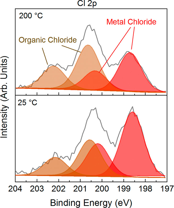
XPS curve fitting of the Cl 2p core level for the oCVD thin films elaborated at 25 and 200 °C. The organic chloride contributions (Cl 2p3/2 = ca. 200.8 eV and Cl 2p1/2 = ca. 202.4 eV) is depicted in brown, alongside the metal chloride contributions (Cl 2p3/2 = ca. 198.7 eV and Cl 2p1/2 = ca. 200.3 eV) in red.
Conclusion
The reaction temperature, i.e., substrate temperature, drastically affects the chemistry and morphology of fused porphyrin thin films prepared from the oCVD reaction of NiDPP and FeCl3. Increase of the reaction temperature notably induces a higher degree of conjugation of the fused porphyrin chains such as evidenced by high-resolution mass spectrometry. While the oCVD thin films elaborated at room temperature are mostly singly fused porphyrins, the one elaborated at 200 °C is mostly composed of doubly fused porphyrins. Beside, higher substrate temperatures also promote the chlorination of the fused porphyrins, known to further decrease the solubility of porphyrins and that might be useful for several applications, including electrocatalysis. In addition, higher reaction temperatures yield a large decrease of the film density and mesoporous morphology, such as observed by helium ion microscopy. This enables water to penetrate the porous structure of the oCVD thin films elaborated at higher temperature in a greater extent, i.e., higher water uptake. The ability to simultaneously synthesize and deposit multiply fused porphyrin thin films possessing high surface area may directly benefit various applications that would combine the fascinating properties of fused porphyrins and high interfacial areas, for example, sensors and heterogeneous catalysis.
Acknowledgments
This project has received funding from the European Research Council (ERC) under the European Union’s Horizon 2020 research and innovation programme (Grant agreement no. 865985). E. Lentzen, Dr. N. Valle, Dr. J. Guillot, and C. Vergne from LIST are acknowledged for the SIMS and XPS measurements.
Supporting Information Available
The Supporting Information is available free of charge at https://pubs.acs.org/doi/10.1021/acsami.0c09630.
Scheme of the oCVD reactor; oCVD reaction conditions; film’s characteristics (thickness, weight, density, conductivity, roughness, modulus, WCA, and water uptake); HIM top view images; optical images of the as-deposited and rinsed films and their soluble phase; UV–vis–NIR spectra of the films; NanoSIMS elemental distribution of 35Cl and 56Fe16O images; height and modulus AFM images, AP-LDI-HRMS spectra and XPS spectra of all the films; schematics of the dimeric triply linked and doubly linked NiDPP species formed during the oCVD reaction of NiDPP (PDF)
The authors declare no competing financial interest.
Supplementary Material
References
- Jia H.; Sun Z.; Jiang D.; Du P. Covalent Cobalt Porphyrin Framework on Multiwalled Carbon Nanotubes for Efficient Water Oxidation at Low Overpotential. Chem. Mater. 2015, 27 (13), 4586–4593. 10.1021/acs.chemmater.5b00882. [DOI] [Google Scholar]
- Hijazi I.; Bourgeteau T.; Cornut R.; Morozan A.; Filoramo A.; Leroy J.; Derycke V.; Jousselme B.; Campidelli S. Carbon Nanotube-Templated Synthesis of Covalent Porphyrin Network for Oxygen Reduction Reaction. J. Am. Chem. Soc. 2014, 136 (17), 6348–6354. 10.1021/ja500984k. [DOI] [PubMed] [Google Scholar]
- Khusnutdinova D.; Wadsworth B. L.; Flores M.; Beiler A. M.; Reyes Cruz E. A.; Zenkov Y.; Moore G. F. Electrocatalytic Properties of Binuclear Cu(II) Fused Porphyrins for Hydrogen Evolution. ACS Catal. 2018, 8 (10), 9888–9898. 10.1021/acscatal.8b01776. [DOI] [Google Scholar]
- Tsuda A.; Osuka A. Fully Conjugated Porphyrin Tapes with Electronic Absorption Bands That Reach into Infrared. Science 2001, 293 (5527), 79–82. 10.1126/science.1059552. [DOI] [PubMed] [Google Scholar]
- Kim D. Y.; Ahn T. K.; Kwon J. H.; Kim D.; Ikeue T.; Aratani N.; Osuka A.; Shigeiwa M.; Maeda S. Large Two-Photon Absorption (TPA) Cross-Section of Directly Linked Fused Diporphyrins. J. Phys. Chem. A 2005, 109 (13), 2996–2999. 10.1021/jp050747h. [DOI] [PubMed] [Google Scholar]
- Algethami N.; Sadeghi H.; Sangtarash S.; Lambert C. J. The Conductance of Porphyrin-Based Molecular Nanowires Increases with Length. Nano Lett. 2018, 18, 4482–4486. 10.1021/acs.nanolett.8b01621. [DOI] [PubMed] [Google Scholar]
- Leary E.; Limburg B.; Alanazy A.; Sangtarash S.; Grace I.; Swada K.; Esdaile L. J.; Noori M.; Gonza M. T.; Rubio-bollinger G.; Higgins S. J.; Lambert C. J.; Sadeghi H.; Hodgson A.; Anderson H. L.; Nichols R. J. Bias-Driven Conductance Increase with Length in Porphyrin Tapes. J. Am. Chem. Soc. 2018, 140, 12877–12883. 10.1021/jacs.8b06338. [DOI] [PubMed] [Google Scholar]
- Wiengarten A.; Seufert K.; Auwärter W.; Ecija D.; Diller K.; Allegretti F.; Bischoff F.; Fischer S.; Duncan D. A.; Papageorgiou A. C.; Klappenberger F.; Acres R. G.; Ngo T. H.; Barth J. V. Surface-Assisted Dehydrogenative Homocoupling of Porphine Molecules. J. Am. Chem. Soc. 2014, 136 (26), 9346–9354. 10.1021/ja501680n. [DOI] [PubMed] [Google Scholar]
- Haq S.; Hanke F.; Sharp J.; Persson M.; Amabilino D. B.; Raval R. Versatile Bottom-Up Construction of Diverse Macromolecules on a Surface Observed by Scanning Tunnelling Microscopy. ACS Nano 2014, 8 (9), 8856–8870. 10.1021/nn502388u. [DOI] [PubMed] [Google Scholar]
- Bengasi G.; Baba K.; Frache G.; Desport J.; Gratia P.; Heinze K.; Boscher N. D. Conductive Fused Porphyrin Tapes on Sensitive Substrates by a Chemical Vapor Deposition Approach. Angew. Chem., Int. Ed. 2019, 58, 2103–2108. 10.1002/anie.201814034. [DOI] [PMC free article] [PubMed] [Google Scholar]
- Baba K.; Bengasi G.; El Assad D.; Grysan P.; Lentzen E.; Heinze K.; Frache G.; Boscher N. D. Conductive Directly Fused Poly(Porphyrin) Coatings by Oxidative Chemical Vapour Deposition – From Single- to Triple- Fused. Eur. J. Org. Chem. 2019, 2019 (13), 2368–2375. 10.1002/ejoc.201900045. [DOI] [Google Scholar]
- Tanaka T.; Osuka A. Conjugated Porphyrin Arrays: Synthesis, Properties and Applications for Functional Materials. Chem. Soc. Rev. 2015, 44 (4), 943–969. 10.1039/C3CS60443H. [DOI] [PubMed] [Google Scholar]
- Tanaka T.; Osuka A. Triply-Linked Porphyrinoids. Chem. - Eur. J. 2018, 24 (65), 17188–17200. 10.1002/chem.201802810. [DOI] [PubMed] [Google Scholar]
- Bengasi G.; Desport J. S.; Baba K.; Cosas Fernandes J. P.; De Castro O.; Heinze K.; Boscher N. D. Molecular Flattening Effect to Enhance the Conductivity of Fused Porphyrin Tape Thin Films. RSC Adv. 2020, 10 (12), 7048–7057. 10.1039/C9RA09711B. [DOI] [PMC free article] [PubMed] [Google Scholar]
- Bengasi G.; Quétu L.; Baba K.; Ost A.; Fernandes P. C.; Grysan P.; Heinze K.; Boscher N. D. Constitution and Conductivity of Metalloporphyrin Tapes. Eur. J. Inorg. Chem. 2020, 2020 (20), 1938–1945. 10.1002/ejic.202000243. [DOI] [Google Scholar]
- Im S. G.; Kusters D.; Choi W.; Baxamusa S. H.; van de Sanden M. C. M.; Gleason K. K. Conformal Coverage of Poly(3,4- Ethylenedioxythiophene) Films with Tunable Nanoporosity. ACS Nano 2008, 2 (9), 1959–1967. 10.1021/nn800380e. [DOI] [PubMed] [Google Scholar]
- Wirtz T.; De Castro O.; Audinot J.; Philipp P. Imaging and Analytics on the Helium Ion Microscope. Annu. Rev. Anal. Chem. 2019, 12 (1), 523–543. 10.1146/annurev-anchem-061318-115457. [DOI] [PubMed] [Google Scholar]
- Bengasi G.; Baba K.; Back O.; Frache G.; Heinze K.; Boscher N. D. Reactivity of Nickel(II) Porphyrins in OCVD Processes — Polymerisation, Intramolecular Cyclisation and Chlorination. Chem. - Eur. J. 2019, 25, 8313–8320. 10.1002/chem.201900793. [DOI] [PMC free article] [PubMed] [Google Scholar]
- Tsuda A.; Osuka A. Discrete Conjugated Porphyrin Tapes with an Exceptionally Small Bandgap. Adv. Mater. 2002, 14 (1), 75–79. . [DOI] [Google Scholar]
- Boscher N. D.; Wang M.; Gleason K. K. Chemical Vapour Deposition of Metalloporphyrins: A Simple Route towards the Preparation of Gas Separation Membranes. J. Mater. Chem. A 2016, 4 (46), 18144–18152. 10.1039/C6TA08003K. [DOI] [Google Scholar]
- Hooley J. G.; Bartlett M. The Intercalation Isotherm of Ferric Chloride Vapor on Graphite from 300 to 350 °C. Carbon 1967, 5, 417–422. 10.1016/0008-6223(67)90017-6. [DOI] [Google Scholar]
- Hooley J. G.; Sams J. R.; Liengme B. V. The Effect of Flake Size on the Mössbauer Spectrum of Graphite Ferrous Chlorides. Carbon 1970, 8, 467–471. 10.1016/0008-6223(70)90007-2. [DOI] [Google Scholar]
- Borrelli D. C.; Barr M. C.; Bulović V.; Gleason K. K. Bilayer Heterojunction Polymer Solar Cells Using Unsubstituted Polythiophene via Oxidative Chemical Vapor Deposition. Sol. Energy Mater. Sol. Cells 2012, 99, 190–196. 10.1016/j.solmat.2011.11.040. [DOI] [Google Scholar]
- Stamenkovic V. R.; Strmcnik D.; Lopes P. P.; Markovic N. M. Energy and Fuels from Electrochemical Interfaces. Nat. Mater. 2017, 16 (1), 57–69. 10.1038/nmat4738. [DOI] [PubMed] [Google Scholar]
- Tsuda A.; Nakamura Y.; Osuka A. Synthesis of Meso-β Doubly Linked Porphyrin Tapes. Chem. Commun. 2003, 9, 1096–1097. 10.1039/b302032k. [DOI] [PubMed] [Google Scholar]
- Fukumoto H.; Omori Y.; Yamamoto T. Effects of Solvent and Temperature on Regioregularity of Poly(3-Hexylthiophene-2,5-Diyl) Prepared by Chemical Oxidative Polymerization. Polym. J. 2013, 45 (4), 462–465. 10.1038/pj.2012.152. [DOI] [Google Scholar]
- Chen P.; Fang Y.; Kadish K. M.; Lewtak J. P.; Koszelewski D.; Janiga A.; Gryko D. T. Electrochemically Driven Intramolecular Oxidative Aromatic Coupling as a Pathway toward Π-Extended Porphyrins. Inorg. Chem. 2013, 52, 9532–9538. 10.1021/ic401214e. [DOI] [PubMed] [Google Scholar]
- Fang Y.; Koszelewski D.; Kadish K. M.; Gryko D. T. Facile Electrosynthesis of π-Extended Porphyrins. Chem. Commun. 2014, 50, 8864–8867. 10.1039/C4CC02759K. [DOI] [PubMed] [Google Scholar]
- Kang B. K.; Aratani N.; Lim J. K.; Kim D.; Osuka A.; Yoo K.-H. Length and Temperature Dependence of Electrical Conduction through Dithiolated Porphyrin Arrays. Chem. Phys. Lett. 2005, 412, 303–306. 10.1016/j.cplett.2005.07.008. [DOI] [Google Scholar]
- Viola W.; Zhang L.; Andrew T. L. Oxidant Aggregate-Induced Porosity in Vapour-Deposited Polymer Films and Correlated Impact on Electrochemical Properties. Supramol. Chem. 2019, 31 (8), 491–498. 10.1080/10610278.2019.1623892. [DOI] [Google Scholar]
- Sahoo A. K.; Nakamura Y.; Aratani N.; Kim K. S.; Noh S. B.; Shinokubo H.; Kim D.; Osuka A. Synthesis of Brominated Directly Fused Diporphyrins through Gold(III)-Mediated Oxidation. Org. Lett. 2006, 8 (18), 4141–4144. 10.1021/ol061763f. [DOI] [PubMed] [Google Scholar]
- Lewtak J. P.; Gryko D.; Bao D.; Sebai E.; Vakuliuk O.; Scigaj M.; Gryko D. T. Naphthalene-Fused Metallo-Porphyrins–Synthesis and Spectroscopy. Org. Biomol. Chem. 2011, 9, 8178–8181. 10.1039/c1ob06281f. [DOI] [PubMed] [Google Scholar]
Associated Data
This section collects any data citations, data availability statements, or supplementary materials included in this article.


