Abstract
The aim of the study was to prepare SnO2 nanowires via a combination of electrospinning and the sol–gel method from a polyvinylpyrrolidone (PVP)/dimetylformamide (DMF)/ethanol(EtOH)/tin(IV) chloride pentahydrate (SnCl4·5H2O) solution. The morphology, structure and chemical composition of the obtained PVP/SnO2 nanofibers and SnO2 nanowires were examined using transmission electron microscopy (TEM), Fourier transform infrared spectroscopy (FTIR) as well as a scanning electron microscope (SEM) with an energy dispersive spectrometer (EDX). The optical property analysis was performed on the basis of UV–Vis spectra of absorbance as a function of the wavelength, based on which the rated values of band gaps of the fabricated 1D nanostructures were determined. The morphology analysis showed that the obtained amorphous SnO2 nanowires with crystalline protuberances were characterized by a diameter of 50 to 120 nm. Results demonstrated that nanowires with a ratio of 1:1 precursor to polymer in the spinning solution were characterized by the smallest diameter after calcination and the smallest energy gap of 3.3 eV among all investigated samples. The rest of the studied materials were characterized by a larger energy gap (3.8 and 3.9 eV).
Subject terms: Nanowires, Optical materials and structures
Introduction
In recent years, the attention of scientists in the field of nanotechnology has been attracted by one-dimensional (1D) semiconductor nanomaterials based on metal oxides, which due to the large specific surface area, unique optical and electrical properties, can be applied in chemical sensors, batteries, fuel and solar cells, optic and optoelectronic devices or photocatalysis1–8. This group of materials includes SnO2, Bi2O3, TiO2, ZnO9–12. Among the many methods of their preparation such as the sol–gel method, chemical deposition, hydrothermal methods and magnetron sputtering, electrospinning method stands out13–17. The combination of the following two techniques of sol–gel and electrospinning used to prepare inorganic 1D nanostructures from metal oxides is gaining more and more interest due to the high quality of the product, simplicity, low manufacturing costs and a variety of available ceramic materials18,19.
In terms of optical properties, tin oxide is one of the most interesting materials. Tin oxide is a semiconductor with a wide energy gap of about 3.1–3.7 eV (Table 1), it is characterized by optical transparency as well as chemical and thermal stability20,21. This material is successfully produced in the form of thin layers, nanoparticles or porous microstructures, and is used mainly in gas detection, which owes structural stability, easy accessibility, low costs of manufacturing and high gas sensitivity22–27.
Table 1.
Dependence of the energy band gap on the synthesis method and structure of SnO2.
| Material type | Structure | Synthesis method | Band gap (eV) | References |
|---|---|---|---|---|
| Thin films | Amorphous | Atomic layer deposition (ALD) | 3.75 | 23 |
| Thin films | Tetragonal rutile | Spray pyrolysis | 3.96–3.99 | 28 |
| Nanopowder | Tetragonal rutile | Self-propagating high-temperature synthesis (SHS) | 3.58–4.0 | 29 |
| Nanoparticles | Tetragonal rutile | Sol–gel | 3.9 | 30 |
| Nanospheres | Tetragonal rutile | Hydrothermal | 3.7 | 31 |
| Nanorods | 3.55 | |||
| Nanorods | Tetragonal rutile | Low temperature hydrothermal synthesis | 3.88 | 32 |
| Nanowires | Tetragonal rutile | Thermal evaporation | 3.33 | 33 |
| Nanofibers | Tetragonal rutile | Electrospinning | 3.48 | 34 |
| Nanofibers | Tetragonal rutile | Electrospinning | 3.59 | 35 |
| Nanofibers | Tetragonal rutile—amorphous | Electrospinning | 3.3–3.9 | * |
*Presented work: “Synthesis of hybrid amorphous/crystalline SnO2 1D nanostructures: investigation of morphology, structure and optical properties”.
The first reports on the production of SnO2 nanofibers by electrospinning from a solution were presented in 2006 by Dharmaraj with his colleagues. The electrospinning process of PVA, DMF, EtOH and SnCl2·2H2O solution was carried out using fixed parameters: a distance of 16 cm and a potential difference between the electrodes of 15 kV, resulting in composite PVP/precursor nanofibers. These nanofibers were calcined for 4 h at four different temperatures of 300, 400, 500 and 600 °C to assess the effect of the process temperature on the morphology and structure of the obtained materials. SEM and FTIR analysis showed that only the maximum temperature of 600 °C allowed the polymer to be removed to obtain fully crystalline fibers36. Two years later, i.e. in 2008, the work of a Chinese research team was published, in which the preparation of SnO2 nanofibers by electrospinning was presented and the applicability of this nanomaterial as a gas sensor was indicated. The nanofibers were obtained from a mixture of PVA, DMF, EtOH and SnCl4·5H2O using the following process parameters: distance and voltage between the electrodes of 0.5 cm and 5 kV, respectively, after which they were dried at 100 °C for 24 h. Then, the obtained PVA/SnCl4·5H2O nanofibers were annealed at three different temperatures of 300, 500 and 700 °C for 4 h. The authors, after analyzing the morphology of samples obtained from solutions with different PVP concentrations and different annealing temperatures, observed that fine, crystalline samples with a 6% share of PVP, free from defects and with a diameter of approx. 100 nm were obtained by calcination at 700 °C. The properties of the SnO2-coated ethanol detection sensor were tested, and it was shown that the newly developed sensor had a low detection limit, fast response and high repeatability37. In 2009, Qi et al. described a study of the impact of using a P123 block copolymer, as an addition to a spinning solution of PVP, DMF, EtOH and SnCl2·2H2O, on the morphology, structure and detection efficiency of NH3, C2H5OH, and CH3COCH3 by SnO2 nanofibers produced by electrospinning. On the basis of the observation of the morphology, structure and BET specific surface measurement, it was noticed that fibers with the addition of P123 have a diameter comparable to undoped ranging from 80 to 150 nm, but also have a much larger surface to volume ratio, hence much better sensory properties38.
Based on the authors' knowledge and experience, and a review of the literature, it has been noticed that one-dimensional nanomaterials characterized by both crystalline and amorphous structure may exhibit different optical, electrochemical properties as compared to those presented by completely crystalline or amorphous nanomaterials5,12,39–45. Obtaining such a structure depends largely on the calcination temperature. Zhou et al. showed that it is possible to control the crystallinity of Ge2O3 nanofibers using a different range of calcination temperatures—the higher it is, the higher the crystallinity of the nanomaterial42. As already mentioned, there is not much research carried out in this particular field so far, however, existing research indicates that such a combination of structures positively affects the energy band gap and the transition of electrons between energy states12. Therefore, we strive to pay special attention to these types of materials, because due to their unique properties they can be extremely valuable when used in modern optoelectronic devices.
Thus, the essence of the work is to produce hybrid crystalline-amorphous SnO2 nanowires and to determine the effect of the applied parameters of the electrospinning and calcining process on the morphology and structure of one-dimensional SnO2 nanostructures, with particular emphasis on the effect of the structure of this nanomaterial on its optical properties. Hence, in this paper the following studies are presented: characterization of the morphology, structure and chemical composition of the obtained nanomaterials using scanning and transmission electron microscopy (SEM and TEM), X-ray energy dispersion spectroscopy (EDX) and FTIR depending on the concentration of the tin oxide precursor and calcination temperature. In addition, the optical properties were analyzed on the basis of the UV–Vis spectrum and the energy gap for the SnO2 nanowires was calculated.
Materials and methods
In order to prepare the spinning solutions, the following reagents were used: poly(vinylpyrrolidone) (PVP, 99%, Mw = 1,300,000 g·mol−1 provided by Sigma Aldrich) as a polymer matrix, ethanol (EtOH, 99.8% purity, purchased from Avantor Performance Materials Poland), N,N-dimethylformamide (DMF, 99.8% purity) and tin (IV) chloride pentahydrate (SnCl4·5H2O, purity of 98%) as an oxide precursor were purchased from Sigma-Aldrich.
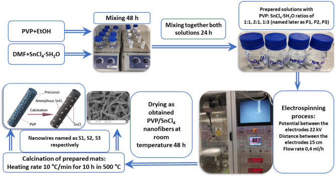
The first step was to prepare four polyvinylpyrrolidone solutions by adding the polymer powder to ethanol in an amount corresponding to 8% wt. relative to the total weight of the solvents and stirring using a magnetic stirrer for 48 h. At the same time, various amounts of tin oxide precursor were dissolved in DMF and after 48 h of stirring was added to the PVP solutions and mixed for another 24 h to obtain homogeneous solutions with an EtOH:DMF mass ratio of 1:1 and PVP:SnCl4·5H2O mass ratio of 2:1, 1:1 and 1:3 (samples were designated as P1, P2 and P3, respectively).
One-dimensional composite PVP/SnCl4 nanostructures were manufactured using FLOW—Nanotechnology Solutions Electrospinner 2.2.0-500 device, with the following parameters: voltage and distance between electrodes, a flow rate of 22 kV, 15 cm and 0.4 ml·h respectively. To degrade the polymer matrix, the obtained composite nanofibers were calcinated in a high-temperature vacuum furnace HT-2100-G-Vac-Graphit-Special, at a 500 °C temperature for 10 h, while the heating rate was 10 °C·min−1 for all samples; after that the samples were left in the furnace to cool. Nanowires corresponding to the ratios mentioned above were designated as S1, S2 and S3, respectively. A scheme summarizing the processes leading to the production of nanowires is shown in Fig. 1.
Figure 1.
Preparation methodology scheme of PVP/SnCl4 nanofibers and SnO2 nanowires.
To investigate the morphology and structure of the produced materials, the (TEM) TITAN 80-300 FEI high-resolution transmission electron microscope was used for imaging in the transmission mode with the use of light and dark field (BF, DF), HAADF detector and filtration of energy, in particular using analytical electron microscopy in nanoareas.
Moreover, to study the effect of the heat treatment of composite PVP/SnCl4·5H2O nanofibers on the topography of the area and to analyze the chemical composition of the prepared samples, the Zeiss Supra 35 scanning electron microscope (SEM) with the EDAX Trident XM4 series X-ray spectrometer (EDX) were used. Based on SEM images, the diameters of the randomly selected composite and ceramic nanowires were measured using the Digital Micrograph. Fourier-Transform Infrared Spectroscopy (FTIR) spectra of the obtained nanomaterials were carried out by the spectrophotometer FTIR Nicolet 6700/8700.
Absorbance measurements have been conducted using the spectrophotometer UV–Vis Evolution 220 by Thermo-Scientific Company.ph software. To investigate the optical properties of the obtained composite and hybrid one-dimensional nanomaterials, the absorbance measurements, as a function of electromagnetic radiation falling on the sample were carried out using UV–Vis Evolution 220 spectrophotometer provided by Thermo-Scientific. Moreover, on the basis of UV–Vis absorption specters, the energy band gap value was determined.
Results
Analysis of morphology and structure
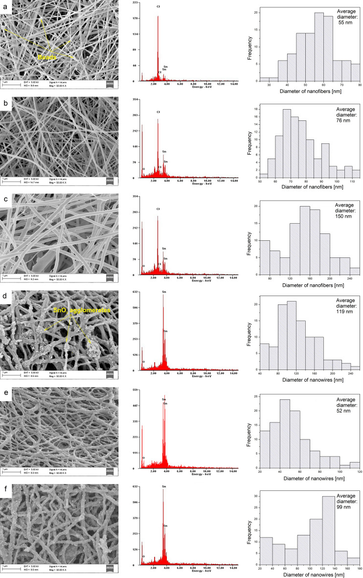
The topographic analysis of composite PVP/SnCl4 nanofibers marked as P2 and P3 revealed that both nanofibrous samples were free from defects in the form of beads, and their diameter was constant over the entire length of the fiber (Fig. 2b,c). Furthermore, the analysis of the P1 sample revealed a small number of beads, as well as glued fibers, which may be related to the hydrolysis and condensation reactions of the precursor at the mixing stage (Fig. 2a). This is a very common defect and at the same time undesirable, however it can be avoided at the preparation stage of the spinning solution by using anhydrous solutions or drying, as well as during electrospinning by controlling the process parameters appropriately41. It was found that all of the composite nanofibers have smooth surfaces and a cylindrical structure with an average diameter of 30–250 nm. This proves the proper viscosity of the spinning solution and the correctly established electrospinning process parameters.
Figure 2.
Left: SEM image of the topography on the surface of the formed fibrous composite mats and obtained bimodal nanowires, histograms presenting the distribution of 100-fold measurement of the diameter of randomly selected: nanofibers obtained from PVP:SnCl4 (a) 2:1, (b) 1:1, (c) 1:3 solutions and (d–f) corresponding them SnO2 nanowires after calcination in 500 °C, obtained EDX spectra from the entire area shown in the SEM images.
A 100-fold measurement of the obtained PVP/SnCl4 random nanofibers confirmed that the diameter of the fibers electrospun from the solution with the lowest concentration of oxide precursor (P1) was the smallest compared to other samples and ranged from 30 to 80 nm, with nanofibers with diameters from 55 to 65 forming the largest group—39% (Fig. 2b). The increase in the precursor amount caused an increase in the diameter of the nanofibers, and in the case of sample P2, nanofibers with diameters in the range between 50–115 nm were observed, and the most common diameter values (also 39% of all measured diameters) were in the 65–85 nm range (Fig. 2c). The largest diameter was found in sample P3 obtained from a solution with six times more precursor than the second one. The nanofibers were characterized by diameters in the range of 60 to 250 nm, of which the most common values were in the 140–180 nm range (Fig. 2c). Therefore, it can be unequivocally stated that the precursor concentration is not without influence on the morphology of PVP/SnCl4 nanofibers.
S2 and S3 nanowires obtained after calcination at a 500 °C temperature, were characterized by a highly developed, rough surface with a large number of protuberances caused by crystallization on the surface, which is presented in Fig. 2e,f. Based on the significant similarity to the morphology of Ga2O3 nanofibers obtained by Zhou et al., S2 and S3 nanowires were found to be amorphous with SnO2 crystals on the surface, which is schematically verified and confirmed later by TEM analysis (Figs. 5, 6)42. The histograms shown in Fig. 2e,f reveal that in the case of both samples of S2 and S3 spinning solution, a decrease in the diameter of the nanowire was observed compared to the diameter of nanofibers before the heat treatment, which results from the degradation of PVP molecules during calcination43. The most numerous group (44%) of nanowires of the second sample were wires with a diameter value in the range of 40–60 nm, while for the third sample, as much as 50% of the measured diameters were in the range of 100–140 nm. In the case of sample S1, large agglomerates of SnO2 were visible on the wires, which results from defects in the form of beads already present before calcining. Moreover, nanowires were sintered together during calcination (Fig. 2d), so that, compared to nanofibers before calcination, a double increase in diameter was noticeable, of which the most common value—41%—was in the range of 80–120 nm (Fig. 2d; Table 2).
Figure 5.
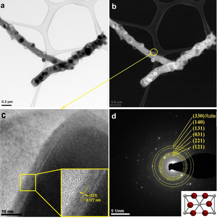
TEM images of the characterized 1D tin oxide nanostructures obtained by calcination P3 sample at 500 °C: (a) in bright field, (b) in dark field, (c) HRTEM of marked area with interplanar distance and (d) diffraction image obtained using STEM mode in selected nanoareas with resolved electronogram and unit cell presentation.
Figure 6.
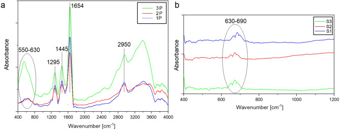
FT-IR spectra of as-prepared PVP/SnCl4 nanofibers and SnO2 nanowires calcined at 500 °C (the spectrum recorded for the nanowires is presented for the 400–1,200 cm−1 range due to background noise above this range).
Table 2.
The average diameter of PVP/SnCl4 nanofibers and SnO2 nanowires depending on the polymer to precursor ratio.
| Type of nanomaterial | The average diameter of nanofibers (nm) | ||
|---|---|---|---|
| 3 (1:3) | 2 (1:1) | 1 (2:1) | |
| Before calcination PVP/SnCl4 | 150 | 55 | 76 |
| After calcination SnO2 | 99 | 119 | 52 |
An analysis of the EDX spectrum of nanofibers obtained from each spinning solution showed the presence of SnCl4 precursor elements (Fig. 2a–c), while the spectra presented in Fig. 2d–f based on the samples after calcination confirmed obtaining pure SnO2 nanowires without the presence of undesirable elements (undescribed peaks near 2.0 eV presents Au and Pt, which were sputtered on the samples, Al comes from foil, and C from conductive carbon tape).
In order to investigate the morphology of the SnO2 nanowires obtained after calcination of PVP/SnCl4 nanofibers, the transmission electron microscope (TEM) characterization was carried out with the results presented in Figs. 3, 4, 5. Figure 3a,b reveal a smooth surface and the absence of any particles or roughness on a single S1 nanowire, which had a diameter of about 540 nm and a length of 3.5 mm. In the high-resolution mode, no distinct lattice planes fringes in the structure could be seen (Fig. 3c). Moreover, reflections on the diffraction spectrum obtained for a single SnO2 nanostructure were diffuse rings (Fig. 3d), which clearly indicates their homogenous amorphous structure.
Figure 3.
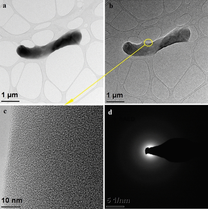
TEM images of the characterized 1D tin oxide nanostructures obtained by calcination P1 sample at 500 °C: (a) in bright field, (b) in dark field, (c) HRTEM of marked area and (d) diffraction image obtained using STEM mode in selected nanoareas.
Figure 4.
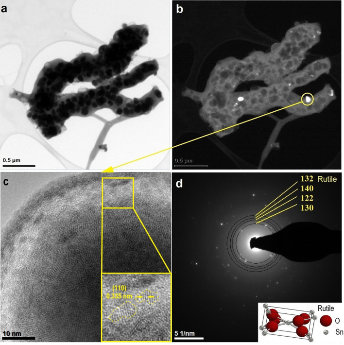
TEM images of the characterized 1D tin oxide nanostructures obtained by calcination P2 sample at 500 °C: (a) in bright field, (b) in dark field, (c) HRTEM of marked area with interplanar distance and (d) diffraction image obtained using STEM mode in selected nanoareas with resolved electronogram and rutile unit cell.
Figure 4 presents TEM analysis for nanowires made from a spinning solution with the lowest precursor concentration, and in contrast to the S1 sample, branched and sintered nanowires with particles inside and on the surface of the nanowires were visible; the diameter of a single nanowire was determined to be 240 nm. In Fig. 4c, at high magnification of a single particle of the surface, it has been observed that an amorphous shell covers the polycrystalline particle and crystallographic lattice planes of different orientation were visible. The electronogram obtained from the area visible in Fig. 4c presents the diffraction image derived from a single particle on the surface of the nanowire and reflections in the form of diffraction rings deriving from the following planes with Miller indices: (130), (122), (140), and (132), which correspond to the tetragonal, rutile structure of SnO2 assigned to the spatial group P 42/m n m no. 136.
In the images taken in the bright and dark fields, two nanowires are visible, their diameter was about 130 nm and their length was about 2 µm, which makes it possible to state that the obtained material could be classified as one-dimensional (Fig. 5a,b). In Fig. 5a, as in the previous sample, dark crystalline protuberances are visible on the light amorphous wire. To further confirm the crystallinities of single surface protuberance, selected area electron diffraction (SAED) patterns were obtained from the area shown in Fig. 5c. Distinct ring patterns were indexed to the polycrystalline tetragonal structure of SnO2 from the following planes with Miller indices: (121), (221), (031), (131), (140) and (330), which were assigned to the spatial group P 42/m n m no. 136 (Fig. 5d).
It has been demonstrated that the nanowire protuberances seen in SEM images were polycrystalline rutile nanoparticles with diameters up to 90 nm, in which crystallization in the amorphous wire has been stopped42. The combination of SEM and TEM analysis allows to state that regardless of the precursor concentration, after calcination at a 500 °C temperature, amorphous SnO2 and amorphous-crystalline SnO2 nanowires were obtained (Figs. 2, 3, 4, 5).
In order to determine the structure of the obtained PVP/SnCl4 and SnO2 nanowires, an analysis using a Fourier-Transform Infrared spectrometer (FTIR) was performed (Fig. 6). In Fig. 6a, the characteristic absorption peaks of PVP were observed at 1,654, 1,445, 1,370 and 1,295 cm−1 which correspond to the vibration of the carbonyl group C=O, O–H bending and -C-N stretching, respectively (Fig. 6a). The strong peak observed at 2,950 cm−1 can be assigned to asymmetric stretching vibration of C–H bending. Moreover, the band at 550–60 cm−1 corresponds to the –Sn–O bond; higher absorbance in this range for sample P3 is associated with the highest concentration of precursor46–48. One visible wide peak in the spectrum recorded for SnO2 nanowires can be observed (Fig. 6b). The band appearing at 630–690 cm−1 is associated with the fundamental –Sn–O bond36.
Analysis of optical properties
In order to investigate the optical properties of 1D SnO2 nanostructures obtained from solutions with three different precursor concentrations, UV–Vis spectral studies were performed. Based on the recorded absorbance spectra as a function of the electromagnetic radiation where the wavelength was in the range of 200–1,100 nm, the optical band gap of the manufactured nanowires was determined.
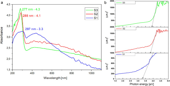
Spectral characteristics recorded for tin oxide nanowires obtained from the second and third solutions showed the presence of a sharp absorption edge in the middle UV region, with the sharp absorption edge wavelength estimated at of 300 nm (Fig. 7a). The absorption maxima were registered with a wavelength of 288 and 277 nm, respectively. In Fig. 7a, it can be seen that the first sample shows a gradual fall in absorption in the UV region, wherein the absorption maxima could be identified at the characteristic wavelength of about 297 nm. The values of absorption edges obtained for SnO2 nanowires are similar to those obtained for SnO2 nanocrystals36,49. Moreover, the decrease in the maximum absorption for the first sample was recorded from 4.3 for the first sample to 3.3 in the middle UV range, which may be due to smaller values of nanowire diameters. Similarly, in the visible light range, a decrease in absorbance to 1.5 was noticed.
Figure 7.
UV–Vis: (a) absorption spectrum of SnO2 nanowires calcined in 500 °C, (b) (αhν)2 versus photon energy (hν) plots, along with matching straights, crossing of which with energy axis corresponds to energy gap values of SnO2 nanowires.
The results of studies on the interaction of SnO2 nanowires with electromagnetic radiation in the 200–1,100 nm range clearly indicate very effective absorption of ultraviolet radiation, which can be applied in photocatalytic reactions, manufacturing photovoltaic cells and layers protecting against radiation in this range.
The optical band gap of the obtained one-dimensional tin oxide nanostructures was determined with the help of the Tauc equation (1)5:
| 1 |
where, α—absorption coefficient, h—Planck constant, υ—electromagnetic radiation frequency, A—constant, hν—photon energy, Eg—energy band gap, ρ—coefficient, the taken value was ½.
Figure 7b presents the determination of the optical energy band gap based on the (αhν)2–(hν) plots. The optical band gaps of SnO2 nanowires obtained from the first, second and third solutions were 3.3, 3.8 and 3.9 eV, respectively. The nanowires marked as S2 and S3 were characterized by a much higher energy gap than the gap presented by S1, due to their smaller diameter size and shift of absorption edge. The hybrid SnO2 nanowires presented in this work have a significantly higher energy gap compared to the gap of other forms of SnO2, for example, in comparison to bulk SnO2 (3.6 eV) or thin films (3.54)38,50. The above results indicate a strong quantum confinement effect in SnO2 one dimensional nanomaterials. This is a typical phenomenon for semiconductor 1D nanostructure in which electrons are free to move in one direction, while quantization occurs in the remaining two directions and it is associated with change in the electronic state of the semiconductor. It leads to the widening of the forbidden band and the decreasing of density of electronic states at the edges of the conduction and valence band. This improves electron transfer between states through the position shift of the conduction band to more negative values51. Favorable optical properties makes them extremely desirable in construction of optoelectronic devices such as novel type dye sensitized solar cells (DSSC). The produced one-dimensional SnO2 nanomaterials can be an alternative to TiO2 as a DSSC photoanode material due to the large surface area and similar optical properties like energy gap and light absorption range45.
Conclusions
In summary, hybrid amorphous-crystalline SnO2 one-dimensional nanomaterials have been successfully prepared by a combination of two techniques: sol–gel and electrospinning from PVP/DMF/EtOH/SnCl4·5H2O solution in order to determine the effect of precursor concentration on their structure, morphology and optical properties. Using the following polymer to precursor ratios: 1:1, 2:1, 1:3, composite PVP/SnCl4 nanofibers were produced in the electrospinning process and then calcined at the temperature of 500 °C for 10 h.
SEM analysis showed that after the heat treatment process, amorphous nanowires with crystalline SnO2 protuberances on the surface were obtained, but only for samples with higher precursor concentrations. Moreover, an increase in diameter from 55 to 150 nm of composite nanofibers with precursor concentration was observed. The nanowires obtained from the solution with the lowest precursor concentration were sintered and clusters of the ceramic phase were visible, which is the result of the presence of beads already in the composite fibrous mats. TEM analysis allowed to confirm that amorphous and amorphous nanowires with polycrystalline SnO2 nanoparticles were manufactured. The presence of Sn–O stretching in the IR spectra and no peaks from the precursor on the EDX spectrum on the samples after calcination at a 500 °C temperature confirmed the formation of tin oxide.
The analysis of the optical properties of the manufactured nanowires was performed based on the absorbance as a function of the wavelength specters using a UV–Vis spectrophotometer. In the spectrum, a high degree of absorption of electromagnetic radiation of the UV range was noticed in all samples. The band gaps of the calcined fabricated nanowires were calculated from optical spectra and ranged from 3.3 to 3.9 eV; the smallest value was obtained for a sample with a 2:1 PVP to precursor ratio, which is lower than other tin oxide nanostructures. Based on these results, it can be deducted that hybrid SnO2 nanowires with excellent optical properties could be used for the fabrication of novel types of solar cells, optoelectronic devices and as a photocatalyst in water treatment.
Acknowledgements
The research presented in this article was financed by the National Science Centre, Poland based on the decision number 2016/23/B/ST8/02045. Moreover publication was supported as a part of the Rector's grant in the area of scientific research and development works. Silesian University of Technology, grant no. 10/010/RGJ20/0346 and 10/010/RGJ20/0345.
Author contributions
W.M.: conceptualization, Investigation, optical property analysis, T.T.: project administration, Supervision. W.S.: investigation, morphology analysis, writing—review and editing, O.P.: writing—review and editing.
Competing interests
The authors declare no competing interests.
Footnotes
Publisher's note
Springer Nature remains neutral with regard to jurisdictional claims in published maps and institutional affiliations.
References
- 1.Yu L, Li C, Ma S, Li Y, Qi L, Yin M, Fan X. Optoelectronic gas sensor sensitized by hierarchically structured ZnO nanorods/Ag nanofibers via on-chip fabrication. Mater. Lett. 2019;242:71–74. [Google Scholar]
- 2.Tonezzer M, Kim JH, Lee JH, Iannotta S, Kim SS. Predictive gas sensor based on thermal fingerprints from Pt-SnO2 nanowires. Sens. Actuators B Chem. 2019;281:670–678. [Google Scholar]
- 3.Liu X, Jiang Y, Li K, Xu F, Zhang P, Ding Y. Electrospun free-standing N-doped C@ SnO2 anode paper for flexible Li-ion batteries. Mater. Res. Bull. 2019;109:41–48. [Google Scholar]
- 4.Haridas AK, Sharma CS, Hebalkar NY, Rao TN. Nano-grained SnO2/Li4Ti5O12 composite hollow fibers via sol-gel/electrospinning as anode material for Li-ion batteries. Mater. Today Energy. 2017;4:14–24. [Google Scholar]
- 5.Matysiak W, Tański T, Zaborowska M. Manufacturing process, characterization and optical investigation of amorphous 1D zinc oxide nanostructures. Appl. Surf. Sci. 2018;442:382–389. [Google Scholar]
- 6.Zheng F, Zhu Z. Preparation of the Au@ TiO2 nanofibers by one-step electrospinning for the composite photoanode of dye-sensitized solar cells. Mater. Chem. Phys. 2017;208:35–40. [Google Scholar]
- 7.Osali S, Esfahani H, Karami H. Effect of Al doping on crystallography and electro-optical properties of ZnO semiconductor thin films prepared by electrospinning. Solid State Sci. 2018;83:90–98. [Google Scholar]
- 8.Suphankij S, Mekprasart W, Pecharapa W. Photocatalytic of N-doped TiO2 nanofibers prepared by electrospinning. Energy Procedia. 2013;34:751–756. [Google Scholar]
- 9.Wang D, et al. J Constructing hierarchical SnO2 nanofiber/nanosheets for efficient formaldehyde detection. Sens. Actuator B Chem. 2019;283:714–723. [Google Scholar]
- 10.Wang C, et al. Electrospinning preparation, characterization and photocatalytic properties of Bi2O3 nanofibers. J. Colloid Interface Sci. 2009;333:242–248. doi: 10.1016/j.jcis.2008.12.077. [DOI] [PubMed] [Google Scholar]
- 11.Someswararao MV, Dubey RS, Subbarao PSV, Singh S. Electrospinning process parameters dependent investigation of TiO2 nanofibers. Results Phys. 2018;11:223–231. [Google Scholar]
- 12.Matysiak W, Tański T. Novel bimodal ZnO (amorphous)/ZnO NPs (crystalline) electrospun 1D nanostructure and their optical characteristic. Appl. Surf. Sci. 2019;474:232–242. [Google Scholar]
- 13.Shaposhnik A, et al. Comparison of ammonia sensing characteristics of individual SnO2 nanowire and SnO2 sol–gel nanocomposite. Procedia Eng. 2014;87:951–954. [Google Scholar]
- 14.Son NT, Noh JS, Park S. Role of ZnO thin film in the vertically aligned growth of ZnO nanorods by chemical bath deposition. Appl. Surf. Sci. 2016;379:440–445. [Google Scholar]
- 15.Zhang KX, et al. Synthesis, structural and optical properties of silver nanoparticles uniformly decorated ZnO nanowires. Chem. Phys. Lett. 2018;698:147–151. [Google Scholar]
- 16.Obreja P, Cristea D, Dinescu A, Romaniţan C. Influence of surface substrates on the properties of ZnO nanowires synthesized by hydrothermal method. Appl. Surf. Sci. 2019;463:1117–1123. [Google Scholar]
- 17.Sirota B, et al. Bismuth oxide photocatalytic nanostructures produced by magnetron sputtering deposition. Thin Solid Films. 2012;520:6118–6123. [Google Scholar]
- 18.Wang C, Shao C, Liu Y, Zhang L. Photocatalytic properties BiOCl and Bi2O3 nanofibers prepared by electrospinning. Scr. Mater. 2008;59:332–335. [Google Scholar]
- 19.Zhao M, et al. Synthesis and optical properties of Mg-doped ZnO nanofibers prepared by electrospinning. J. Alloy Compd. 2010;507:97–100. [Google Scholar]
- 20.Al-Saadi TM, Hussein BH, Hasan AB, Shehab AA. Study the structural and optical properties of Cr doped SnO2 nanoparticles synthesized by sol–gel method. Energy Procedia. 2019;157:457–465. [Google Scholar]
- 21.Subramanyam K, Sreelekha N, Murali G, Reddy DA, Vijayalakshmi RP. Structural, optical and magnetic properties of Cr doped SnO2 nanoparticles stabilized with polyethylene glycol. Phys. B. 2014;454:86–92. [Google Scholar]
- 22.Li QL, Zhang XH, Lin T, Gao KH. Electrical transport properties of polycrystalline SnO2 thin films. J Alloy Compd. 2018;764:295–299. [Google Scholar]
- 23.Bang JH, et al. Effect of microwave irradiation on the electrical and optical properties of SnO2 thin films. Ceram. Int. 2019;45:7723–7729. [Google Scholar]
- 24.Horti NC, et al. Photoluminescence properties of SnO2 nanoparticles: effect of solvents. Optik. 2018;169:314–320. [Google Scholar]
- 25.Zhang J, Gao L. Synthesis and characterization of nanocrystalline tin oxide by sol–gel method. J. Solid State Chem. 2004;177:1425–1430. [Google Scholar]
- 26.Li H, et al. Porous SnO2 hollow microspheres as anodes for high-performance lithium ion battery. Mater. Lett. 2018;217:276–280. [Google Scholar]
- 27.Zhao Y, et al. One-step synthesis of SnO2 hollow microspheres and its gas sensing properties. Mater. Lett. 2014;136:286–288. [Google Scholar]
- 28.Choudhury SP. Facile synthesis of SnO2 thin film by spray pyrolysis technique, investigation of the structural, optical, electrical properties. Mater. Today Proc. 2016;3:1609–1619. [Google Scholar]
- 29.Kamarulzaman N, et al. Anomalies in wide band gap SnO2 nanostructures. J. Solid State Chem. 2019;277:271–280. [Google Scholar]
- 30.Ahmed AS, Singla ML, Tabassum S, Naqvi AH, Azam A. Band gap narrowing and fluorescence properties of nickel doped SnO2 nanoparticles. J. Lumin. 2011;131:1–6. [Google Scholar]
- 31.Li S, Yu L, Man X, Zhong J, Liao X, Sun W. The Synthesis and band gap changes induced by the doping with rare-earth ions in nano-SnO2. Mater. Sci. Semicond. Process. 2017;71:128–132. [Google Scholar]
- 32.Inderan V, et al. Synthesis and characterisations of SnO2 nanorods via low temperature hydrothermal method. Superlatt. Microst. 2015;88:396–402. [Google Scholar]
- 33.Kumar V, et al. Copper doped SnO2 nanowires as highly sensitive H2S gas sensor. Sens. Actuator B Chem. 2009;138:587–590. [Google Scholar]
- 34.Bakr Z, et al. Synergistic combination of electronic and electrical properties of SnO2 and TiO2 in a single SnO2–TiO2 composite nanofiber for dye-sensitized solar cells. Electrochim. Acta. 2018;263:524–532. [Google Scholar]
- 35.Wang K, Qian Z, Guo W. Multi-heterojunction of SnO2/Bi2O3/BiOI nanofibers: Facile fabrication with enhanced visible-light photocatalytic performance. Mater. Res. 2019;111:202–211. [Google Scholar]
- 36.Dharmaraj N, Kim CH, Kim KW, Kim HY, Suh EK. Spectral studies of SnO2 nanofibres prepared by electrospinning method. Spectrochim. Acta A. 2006;64:136–140. doi: 10.1016/j.saa.2005.07.007. [DOI] [PubMed] [Google Scholar]
- 37.Zhang Y, He X, Li J, Huang F. Fabrication and ethanol-sensing properties of micro gas sensor based on electrospun SnO2 nanofibers. Sens. Actuator B Chem. 2008;132:67–73. [Google Scholar]
- 38.Qi Q, Zhang T, Liu L, Zheng X, Lu G. Improved NH3, C2H5OH, and CH3COCH3 sensing properties of SnO2 nanofibers by adding block copolymer P123. Sens. Actuator B Chem. 2009;141:174–178. [Google Scholar]
- 39.Matysiak W, Tański T. Analysis of the morphology, structure and optical properties of 1D SiO2 nanostructures obtained with sol-gel and electrospinning methods. Appl. Surf. 2019;489:34–43. [Google Scholar]
- 40.Jarka P, Tański T, Matysiak W, Krzemiński Ł, Hajduk B, Bilewicz M. Manufacturing and investigation of surface morphology and optical properties of composite thin films reinforced by TiO2, Bi2O3 and SiO2 nanoparticles. Appl. Surf. 2017;424:206–212. [Google Scholar]
- 41.Tański T, Matysiak W. Synthesis of the novel type of bimodal ceramic nanowires from polymer and composite fibrous mats. Nanomaterials. 2018;8:179. doi: 10.3390/nano8030179. [DOI] [PMC free article] [PubMed] [Google Scholar]
- 42.Zhou T, et al. Enhanced yellow luminescence of amorphous Ga2O3 nanofibers with tunable crystallinity. Ceram. Int. 2016;42:6467–6474. [Google Scholar]
- 43.Ma LA, Wei ZH. Field emission properties of crystalline-SnO2 (core)/amorphous-SnO2 (shell) nanowire arrays on carbon paper. Mater. Lett. 2018;213:257–261. [Google Scholar]
- 44.Yu Y, Gu L, Dhanabalan A, Chen CH, Wang C. Three-dimensional porous amorphous SnO2 thin films as anodes for Li-ion batteries. Electrochim. Acta. 2009;54:7227–7230. [Google Scholar]
- 45.Li L, et al. Electrospun porous SnO2 nanotubes as high capacity anode materials for lithium ion batteries. Electrochem. Commun. 2010;12:1383–1386. [Google Scholar]
- 46.Du JS. Synthesis of poly (N-vinylpyrrolidone) nanofibers containing gold nanoparticles via electrospinning technique. Chem. Res. Chin. Univ. 2007;23:538–540. [Google Scholar]
- 47.Deniz AE, Vural HA, Ortaç B, Uyar T. Gold nanoparticle/polymer nanofibrous composites by laser ablation and electrospinning. Mater. Lett. 2011;65:2941–2943. [Google Scholar]
- 48.Morales FL, Zayas T, Contreras OE, Salgado L. Effect of Sn precursor on the synthesis of SnO2 and Sb-doped SnO2 particles via polymeric precursor method. Front. Mater. Sci. 2013;7:387–395. [Google Scholar]
- 49.Gu F, et al. Synthesis and luminescence properties of SnO2 nanoparticles. Chem. Phys. Lett. 2003;372:451–454. [Google Scholar]
- 50.Gorley PM. SnO2 films: formation, electrical and optical properties. Mater. Sci. Eng B Adv. 2005;118:160–163. [Google Scholar]
- 51.Kumar, D. S., Kumar, B. J., Mahesh, H. M. Quantum nanostructures (QDs): an overview. In Synthesis of Inorganic Nanomaterials 59–88 (Woodhead Publishing, 2018).


