Abstract
Direct laser writing, a nano 3D-printing approach, has enabled fabrication of customized carbon microelectrode sensors for neurochemical detection. However, to detect neurotransmitters in tiny biological organisms or synapses, sub-micron nanoelectrodes are required. In this work, we used 3D-printing to fabricate carbon nanoelectrode sensors. Customized structures were 3D-printed and then pyrolyzed, resulting in free-standing carbon electrodes with nanotips. The nanoelectrodes were insulated with atomic layer deposition of Al2O3 and the nanotips were polished by focused ion beam to form 600 nm disks. Using fast-scan cyclic voltammetry, the electrodes successfully detected stimulated dopamine in adult fly brain, demonstrating they are robust and sensitive to use in tiny biological systems. This work is the first demonstration of 3D-printing to fabricate free-standing carbon nanoelectrode sensors, and will enable batch-fabrication of customized nanoelectrode sensors with precise control and excellent reproducibility.
Keywords: 3D-printing, Carbon, Nanoelectrode, Neurotransmitter, Sensors, Two-photon lithography
Graphical Abstract
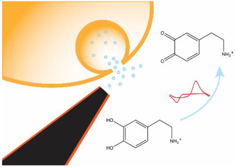
Carbon-based electrodes are favored as electrochemical sensors for neurotransmitter detection because of their conductivity, biocompatibility, and surface structures, which adsorb many electroactive neurotransmitters.1–3 For implantable sensors, a small overall size is necessary to reduce tissue damage and nanometer-scale electrodes are required to measure neurotransmitters at single vesicles or in synapses.4,5 In addition, many smaller organism are now being studied, such as Drosophila, which have brain structures on the scale on microns.6,7 However, it is challenging to fabricate these extremely tiny electrochemical probes with high reproducibility.
In recent years, several approaches have been developed to fabricate carbon nanoelectrode sensors for real-time monitoring of neurochemicals. Carbon fibers, with 7–10 μm diameters, are the conventional electrode material for real-time monitoring of neurotransmission,8,9 and they can be etched to sub-micron scale.10–15 For example, the Huang group developed a flame-etched, carbon-fiber nanoelectrode, and used amperometry to monitor vesicular exocytosis inside individual synapses.11 The Ewing group used similar methods to fabricate carbon-fiber nanotip electrodes, and measured the catecholamine content of single vesicles in PC12 cells.12 However, manual etching, either flame or electrochemical,10–13 lacks precise control of the size and shape of the nanotip. In addition, insulation is difficult and often increases the tip size 2-fold, as they used thicker capillaries or wax.11,13 A different design is to make carbon nanopipettes from quartz capillaries as templates, and selectively deposit carbon on the inner wall by chemical vapor deposition.16–19 Our group used carbon nanopipette electrodes to characterize dopamine in Drosophila.16 To expose the carbon nanotip, the end of quartz capillary was wet-etched by hydrofluoric acid, but this method also lacks precise control of the length of the carbon nanotip. Thus, better methods are needed for high precision and reproducible batch manufacturing of nanoelectrodes, and a precise insulation method is required to insulate while maintaining the overall size in nanoscale.
The development of nano 3D-printing, or direct laser writing, enables a completely new approach to fabricate tiny structures. Customized patterns are printed in polymerized photoresist by a focused, ultrashort, pulsed laser that directly writes by causing polymerization within a small volume (a voxel) of the photopolymer due to two-photon absorption.20–22 Then the volume not exposed to laser is removed by a developer bath, leaving the designed, polymerized structure.23 Pyrolysis turns the polymerized photoresist to carbon, providing a glassy-carbon-like surface, which is beneficial for electrochemical applications.24,25 During pyrolysis, the polymer shrinks while retaining the geometry. The shrinkage is up to 80% in size, which further improves the resolution of 3D direct-laser-written structures.25,26 Direct laser writing usually requires a large substrate to write on, and adaptation to printing free-standing nanostructures remains difficult because you must create a connection between the printed structure and free-standing substrate, and also because of the deformation during pyrolysis.25,26
In this work, we used direct laser writing for the first time to 3D-print free-standing carbon nanoelectrodes and used them as implantable sensors for neurotransmitter detection. The free-standing nanotip was directly 3D-printed onto metal wires, and carbonized by pyrolysis. The carbon nanostructures were further insulated by atomic layer deposition of Al2O3, and polished to disk-shape by focused ion beam. The carbon nanoelectrodes exhibited promising electrochemical activity, and were used for the detection of dopamine in adult fruit fly brains. The novel fabrication method enables fabrication of carbon nanoelectrodes in a precisely controlled, highly reproducible manner, and it has promising potential for rational design of nanoelectrodes for different applications.
Figure 1 shows the procedure for fabricating the carbon nanoelectrodes. The workflow was adapted from our previous work to fabricate 3D-printed microelectrode sensors.24 Metal wires were immobilized on a silicon chip, and a droplet of the IP-S photoresist added to cover the wires. Two-photon lithography was performed by Photonic Professional GT (Nanoscribe, Gmbh.) direct laser writing system, and SU-8 developer was used to remove the volume not cross-linked. The printed structure is micron-scale at the base, to attach to the wire, and sub-micron at the end of the long tip (Figure 1a and Figure S1).24 The polymer structures are pyrolyzed by rapid thermal processing (Figure 1b), resulting in a glassy-carbon-like surface. The structure shrinks about 3-fold in size during pyrolysis, while the geometry is retained. Then a 100 nm layer of Al2O3 is coated using atomic layer deposition (ALD) to insulate the electrodes (Figure 1c). The very end of the nanotip is milled away by focused ion beam (FIB) under scanning electron spectroscopy (SEM), creating disk-shaped carbon nanoelectrodes (Figure 1d).
Figure 1.
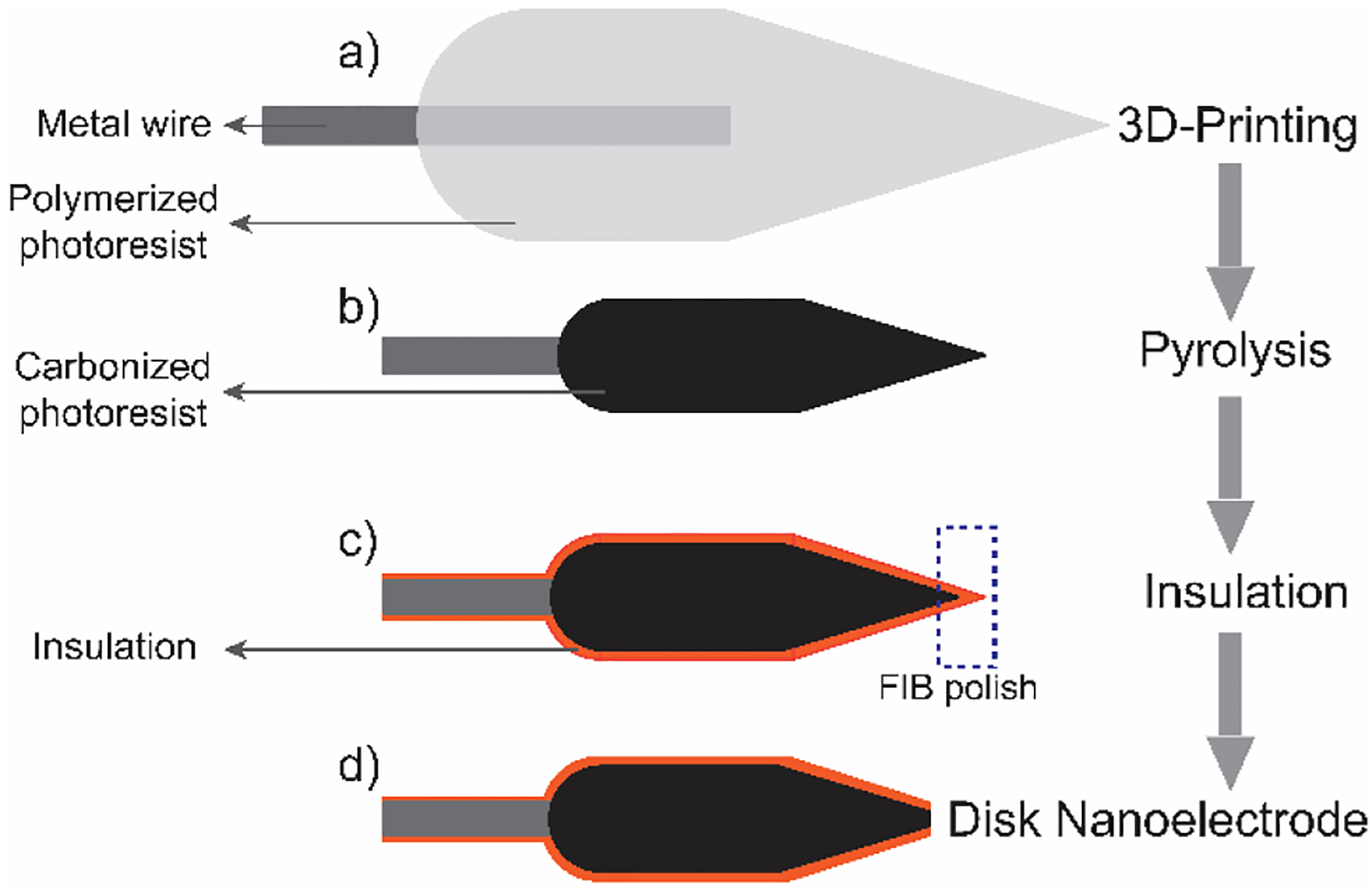
Illustration for the fabrication of 3D-printed carbon nanoelectrodes.
The 3D-printed electrodes were characterized by SEM (Figure 2). We designed a conical structure to form the nanotip with a larger cylindrical base to connect to the metal wire. Two types of structures, a conical geometry (Geometry 1, Figure 2a) and sharper, more tapered cone (Geometry 2, Figure 2b) were fabricated to prove the feasibility of tunable geometry. Table S1 lists the parameters at the base, which show they the printed structures are very close to the design. After pyrolysis, the structures shrank about 3-fold (Table S1), while maintaining the geometries (Figure 2c,d), similar to previous work with the same photoresist.24,27
Figure 2.
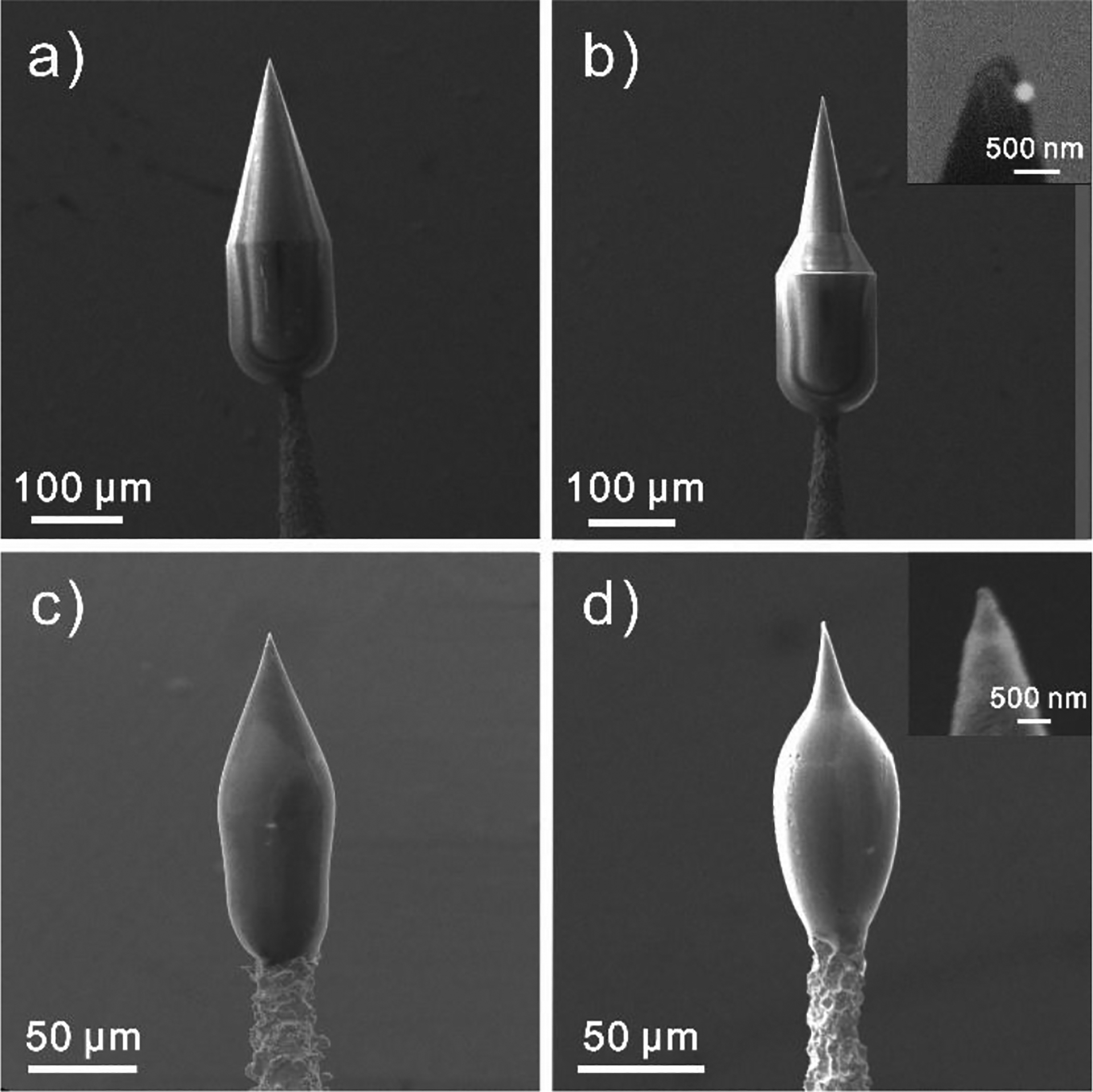
SEM images of 3D-printed structures. Before pyrolysis: a) 3D-printed normal conical geometry (G1), b) 3D-printed sharper conical geometry (G2). After pyrolysis: c) Carbonized G1 and d) Carbonized G2. Inset: zoomed in SEM images around the nanotips.
Table 1 gives the tip properties for the two geometries, including the angle of the tip and the tip width. Geometry 1 is less tapered than geometry 2, thus those electrodes have a larger apex angle. After pyrolysis, the apex angle was not significantly different (unpaired t-test, p < 0.001), indicating the geometry was not changed. The size of the tip is approximately 500 nm as printed, which matches the resolution we used to print it (500 nm between printing layers). The tip shrank about 2-fold during pyrolysis, so the carbon tip size (260 nm) is smaller than the printing size.
Table 1.
Size and shrinkage measurement of the electrode tip.
| Apex angle, printed (°) | Apex angle, pyrolyzed (°) | Tip size, printed (nm) | Tip size, pyrolyzed (nm) | |
|---|---|---|---|---|
| G1 | 27.4 ± 0.4 | 29.2 ± 1.7 | 505 ± 22 | 288 ± 17 |
| G2 | 19.8 ± 0.5 | 20.2 ± 1.6 | 500 ± 35 | 261 ± 29 |
Values are mean ± standard error of the mean, n = 6.
One limitation to fabricate more tapered nanoelectrodes is the structural stability during pyrolysis. When the 3D-printed polymerized structure reaches the nanometer-scale, curling happens due to asymmetric strains caused by nonuniform laser exposure.28,29 Here, the tapers were optimized to prevent curling, and in the future it could be prevented by mounting the structures with spatial restrictions.30
Raman spectra were collected to prove the structures were fully carbonized (Figure S2). The existence of both D band (~1340 cm−1) and G band (~1580 cm−1) indicates the surface is amorphous carbon.31 The high D/G ratio reveals an edge-plane rich surface, which is beneficial to neurochemical detection.32,33 The two different geometries of carbon electrodes show similar D/G ratios, indicating the surface structure of the pyrolyzed carbon is not dependent on the geometry designed.
To insulate the carbon structures to form nanoelectrodes, we used ALD to coat the electrodes, and then used FIB to remove the tip to make a disk-shaped nanoelectrode. Plasma-assisted ALD was performed using trimethylaluminum (TMA) as precursor,34 and a 100 nm thick Al2O3 layer was uniformly coated onto the entire structure (Figure S3). Then the very end of the nanotip was milled by FIB to expose a carbon nanodisk. Figure 3 shows the SEM images during the polishing process. Two electron detectors, a normal SEM detector and a detector to conduct FIB, were aligned at 52° (Figure 3a) and both of them were used to acquire SEM images. Figure 3b and Figure 3c show the SEM images using FIB detector, which was vertical to the nanotip samples. The tip was milled away where the diameter was measured at 600 nm (Figure 3a,b), removing the carbon and aluminum coating (Figure 3c). Figure 3d and Figure 3e show the images taken by SEM detector, revealing the carbon nanodisk after milling. For each sample, the average FIB milling time is less than a minute. The average diameter of the carbon disk was 590 ± 70 nm (n = 4), which matches with our pre-set value of 600 nm. The tip size can be customized by choosing the milling position.
Figure 3.
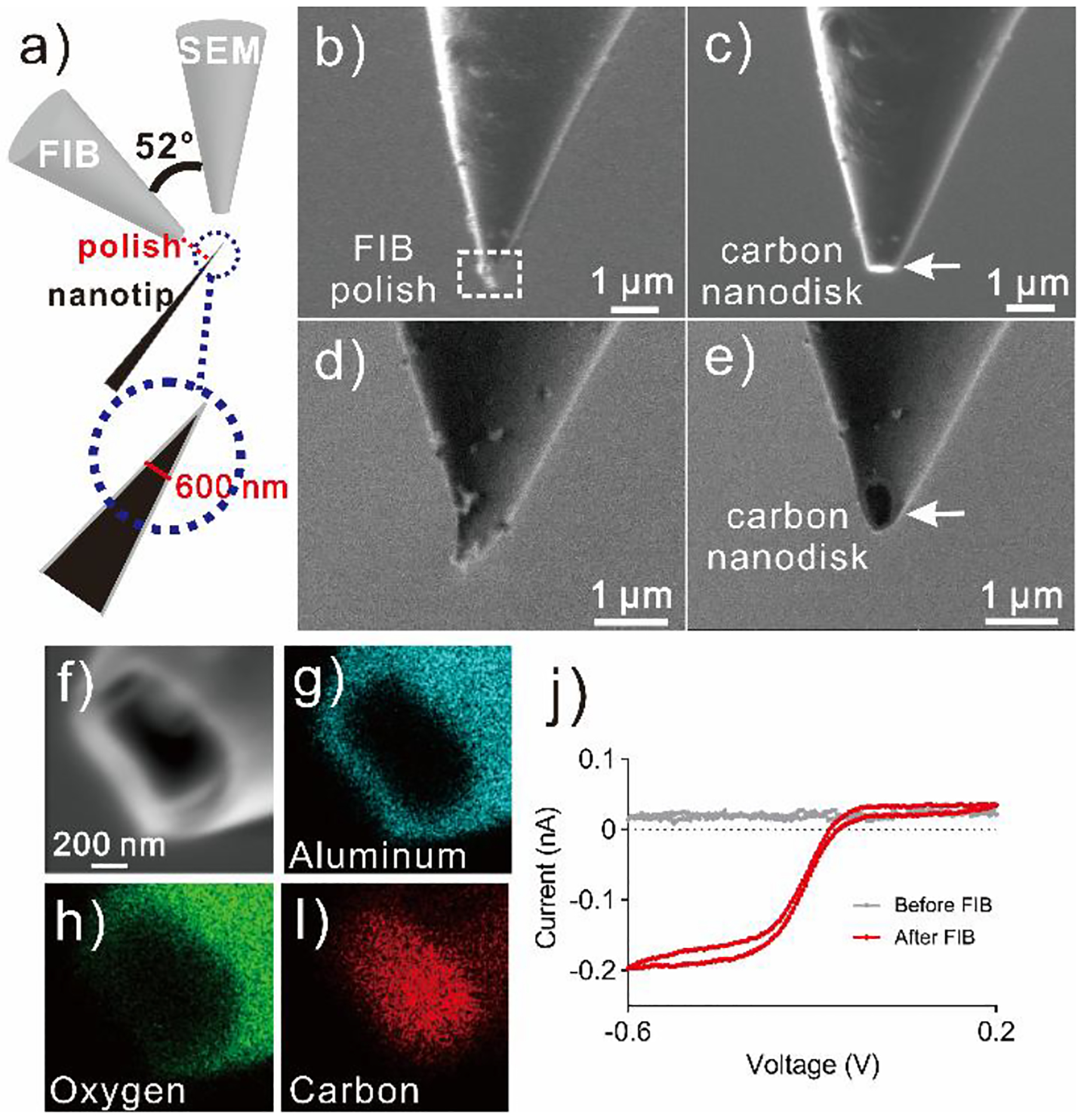
FIB polishing. a) Illustration of sample setup. FIB detector is vertical to the nanotip sample, and SEM detector has an angle of 52 degree with FIB detector. FIB detector view: b) before FIB polish, c) after FIB polish; SEM detector view: d) before FIB polish, e) after FIB polish. f) Zoomed in SEM image of electrode nanotip, g-i) EDS element mapping of g) Aluminum, h) Oxygen and i) Carbon. j) Cyclic voltammogram of the nanoelectrodes before and after FIB polishing in 10 mM Ru(NH3)6Cl3. Scan rate =100 mV s−1.
To prove the effectiveness of the ALD coating and FIB polishing, we collected element mappings of the nanoelectrodes using energy dispersive spectroscopy (EDS). We mapped the element distribution around the electrode nanotip (Figure 3f), including aluminum (Figure 3g), oxygen (Figure 3h), and carbon (Figure 3i). Aluminum and oxygen were located on the side, indicating the Al2O3 coating was effective and uniform. Carbon was located mostly on the nanodisk, where carbon was exposed after FIB polishing. There was also a trace of carbon on the side coating, probably due to the carbon residue in the trimethylaluminum precursor during the ALD coating step.35 We also performed cyclic voltammetry to examine the coating, using the typical surface-insensitive compound Ru(NH3)6Cl3.2 There was no faradaic current response before FIB polishing, indicating the Al2O3 insulation layer was effective. After FIB polishing, the cathodic current was about 200 pA for 10 mM Ru(NH3)6Cl3, comparable to results from previous research on carbon-fiber nanotip electrodes.11,36
While we used Al2O3 as the primary insulation strategy, we also explored insulation by parylene.37 Parylene was coated with vacuum deposition to a thickness of 130 nm. The parylene coated electrodes showed similar results as Al2O3 coated electrodes (Figure S4), so parylene can be used as alternative. Parylene is also biocompatible.38
The carbon nanoelectrodes were characterized by fast-scan cyclic voltammetry (FSCV), which is a standard technique for real-time measurement of neurotransmitters. Figure 4a shows a typical background charging current,9 which is smaller than 1 nA. Carbon-fiber microelectrodes typically have background currents in the hundreds of nA, indicating that the surface area of this electrode is much smaller than typical electrodes. Similarly, the background-subtracted current for 10 μM dopamine is also much smaller than CFMEs (Figure 4b). Dopamine is oxidized to dopamine-o-quinone around 0.6 V and the reduction occurs around −0.1 V,9 and the CV shape is characteristic of dopamine at carbon electrodes. The limit of detection (LOD) for dopamine was 177 ± 21 nM (n = 5). Current is proportional to surface area, so the LOD for the 3D printed nanoelectrode is larger than LOD of a carbon fiber (20 ± 4 nM) or 3D-printed microelectrode (11 ± 1 nM).24 Also, the dopamine current is so small that the normal FSCV potentiostat is not optimized to detect it, as the lowest current detectable is 1 pA. Future improvements in electronics might also reduce the LOD. However, this LOD is acceptable to detect stimulated dopamine in animal brains,39,40 especially since smaller electrodes can get closer to the release site such as synapses, where concentrations are higher.41
Figure 4.
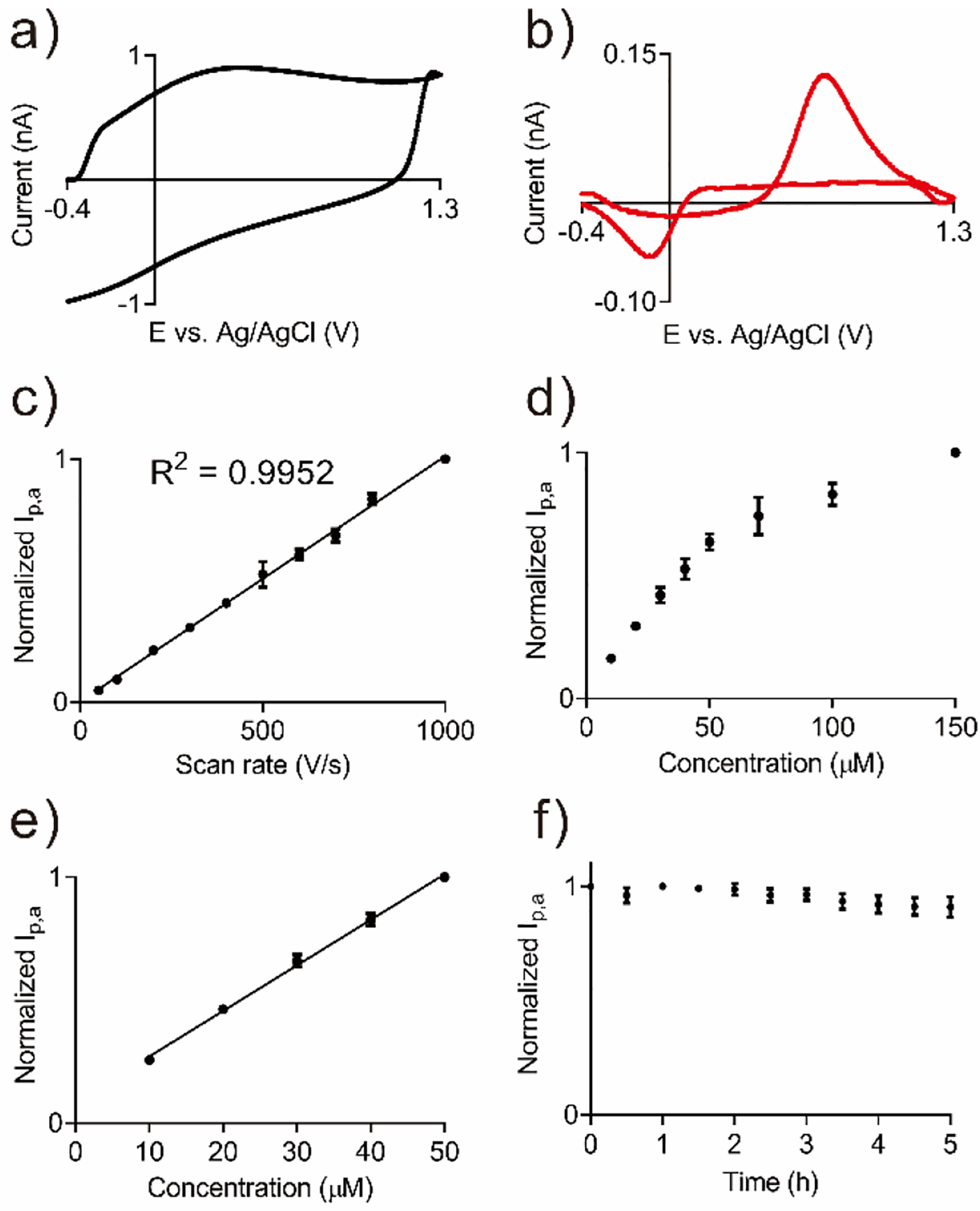
FSCV study of 3D-printed nanoelectrodes. a) Background current. b) Background-subtracted current of 10 μM dopamine. c) Dopamine current is linear with scan rate (R2 = 0.9952, n = 3). d) Dopamine current when concentration is varied from 10 μM to 150 μM (n = 3). e) Dopamine current is linear with concentration up to 50 μM (R2 = 0.9947), f) Stability test. 10 μM dopamine was injected every 0.5 h for 5 h (n = 3).
Figure 4c shows dopamine current increases linearly with scan rate, indicating the kinetics are controlled by adsorption.9 Figure 4d–e shows dopamine anodic current is linear with concentration up to 50 μM. At concentrations above 50 μM, the electrode surface is saturated with adsorbed dopamine, so the kinetics are controlled by diffusion.32 To test the stability of the nanoelectrodes, 10 μM dopamine was detected every half an hour over a 5 h time period, while the FSCV waveform was continually applied (Figure 4f). Anodic peak current did not significantly change during the time period, so electrodes are stable for the length of typical biological experiments.
To prove the 3D-printed nanoelectrodes can be used for measurements of neurotransmitters in tiny biological systems, we used nanoelectrodes to detect dopamine in mushroom body of adult Drosophila. One neuropil of the mushroom body is about 10 μm wide so the typical 7 μm carbon fiber electrodes could destroy or displace the tissue.6 The electrode was positioned at the corner of the mushroom body of a dissected out adult brain, and a micropipette was inserted at the same depth but approximately 10−15 μm away from the tip of the electrode (Figure 5a).42 Figure S5 shows the detection of exogenously-applied dopamine from the pipette. At 5 seconds, exogenous dopamine was applied and the peak current increased dramatically, then slowly decayed due to diffusion and uptake. Figure 5 shows stimulation of endogenous dopamine release by acetylcholine, with a false color plot that shows all the data (Fig. 5b). Time is on the x-axis, potential is on the y-axis and current is shown in false color. The green color represents oxidative current while the blue color represents reduction current. Figure 5c shows a concentration versus time trace, collected by taking a horizontal trace on the false color plot at oxidation peak. At 10 seconds, 2 pmol acetylcholine was applied and dopamine current rose immediately after the stimulation. Figure 5d shows a characteristic cyclic voltammogram for dopamine. The detection of dopamine in adult fly brain demonstrates the 3D-printed nanoelectrodes are implantable in a tiny biological environment in vivo, and they are sensitive enough to detect endogenous dopamine release.
Figure 5.
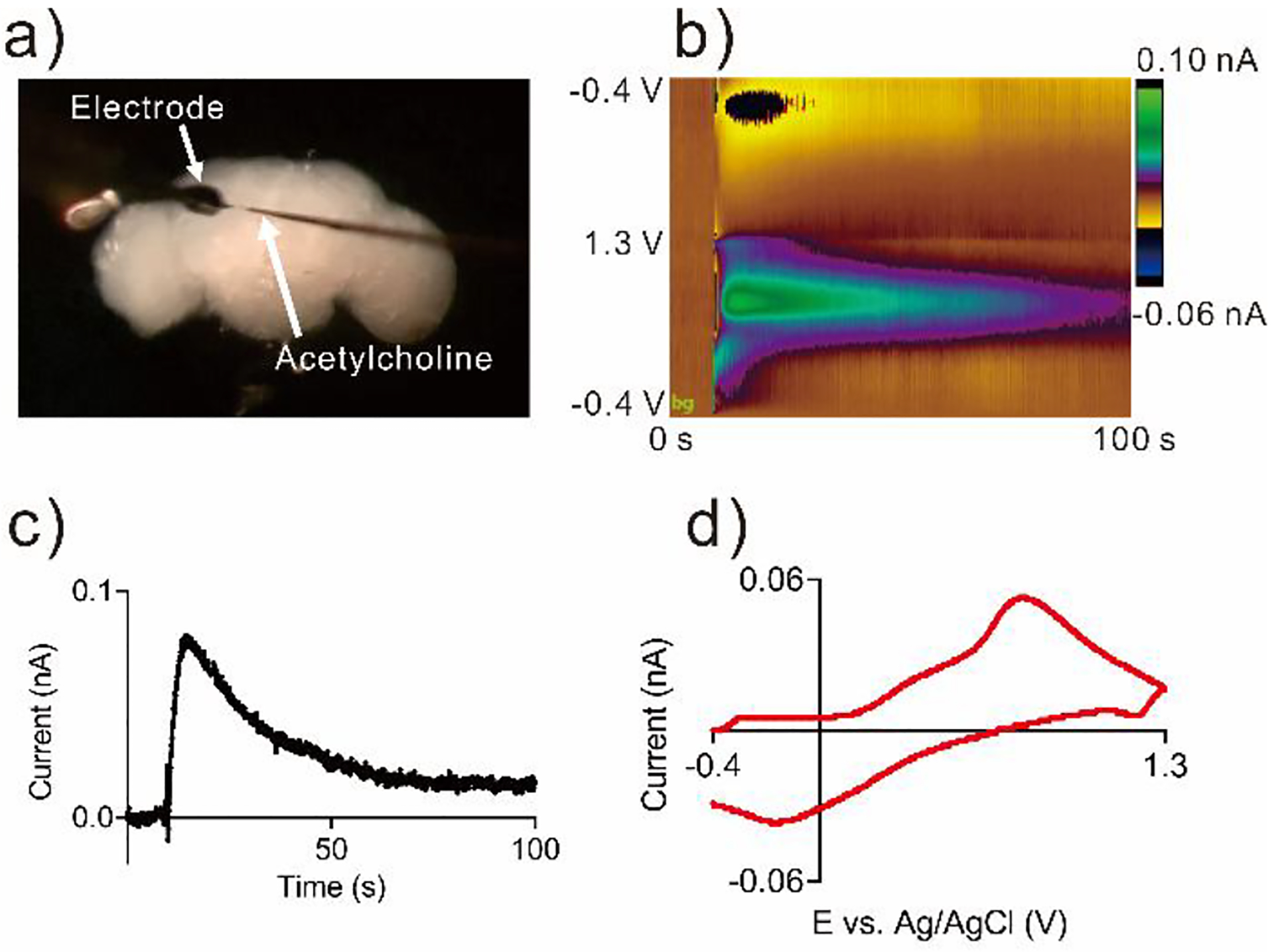
Detection of endogenous dopamine in adult fruit fly brain. a) Microscopy image of adult brain with the 3D-printed nanoelectrode and a micropipette loaded with acetylcholine. b) False color plot of dopamine detected after acetylcholine (2 pmol) stimulation. c) Current response over time for dopamine during stimulation. d) Cyclic voltammogram of the stimulated dopamine.
This is the first time 3D-printing was used to fabricate implantable carbon nanoelectrodes. 3D-printing enables fully customizable electrode geometry with precise control, allowing rational design of nanosensors to adapt to complex biological environment. In contrast, current methods for making nanoelectrodes such as electrochemical and flame etching are not precise,11,14 and cannot achieve customizable, reproducible geometries. The aluminum oxide insulation method is also novel because it facilitates nanoscale insulation, so total tip size is still small. The nanoscale electrode tip allows the measurement of neurotransmitters in small organisms, such as Drosophila, which has brain structures that are only 10 μm wide. In the future, 3D-printed nanoelectrodes would be useful to detect neurochemicals at single cells or near synapses. The design can be optimized to decrease the nanotip size or the apex angle, and nanostructures could be mounted with spatial restrictions to solve some problems with deformation during pyrolysis.30 In addition to fabrication neurochemical electrochemical sensors, 3D printing fully-customized nanoelectrodes is an innovative platform, leading to broad applications.43,44 For example, 3D printed nanoelectrodes would be useful as scanning electrochemical microscopy (SECM) tips in electrochemical imaging45 or for investigating catalytic responses of atom clusters.46
In summary, we have successfully fabricated free-standing 3D-printed carbon nanoelectrodes, and characterized them for dopamine detection. The electrodes were fully-customizable in size and geometry, and batch-manufacturing was highly reproducible. We demonstrated an insulation strategy of ALD of Al2O3, followed by FIB to polish the electrode into a nanodisk. The pyrolyzed tips of the carbon nanoelectrodes were about 260 nm at the nanotip, and they were polished to disk nanoelectrodes with a diameter of 600 nm. Pyrolyzed carbon from cross-linked photoresist is electroactive for neurotransmitter detection, and the 3D-printed nanoelectrodes are robust for implantation into tissue. We successfully used the nanoelectrode to detect dopamine in adult fruit fly brain. Overall, 3D-printing is a promising strategy to fabricate nanoelectrodes sensors as implantable neural devices.
Supplementary Material
ACKNOWLEDGMENT
This work was funded by NIH R01EB026497 and NIH R01MH085159. Direct laser writing, rapid thermal processing, atomic layer deposition, parylene coating, Raman spectroscopy and a portion of scanning electron microscopy of this research were conducted at the Center for Nanophase Materials Sciences, which is a DOE Office of Science User Facility.
Footnotes
Supporting Information
Methods: CAD model of the electrode designs (Figure S1), Detailed fabrication method of 3D-Printed Nanoelectrodes, Pyrolysis, SEM, FIB, EDS, Raman Spectroscopy, Atomic Layer Deposition, Parylene Coating, Cyclic Voltammetry and Fast-scan Cyclic Voltammetry and Fruit Fly Experiments. Raman Spectra (Figure S2), size and shrinkage measurements of the base of the electrodes (Table S1), SEM image of ALD coating (Figure S3) and data of parylene coating (Figure S4), and detection of exogenous dopamine in adult fruit fly brain (Figure S5).
The authors declare no competing financial interest.
REFERENCES
- (1).Cao Q; Puthongkham P; Venton BJ Review: New Insights into Optimizing Chemical and 3D Surface Structures of Carbon Electrodes for Neurotransmitter Detection. Anal. Methods 2019, 11 (3), 247–261. 10.1039/c8ay02472c. [DOI] [PMC free article] [PubMed] [Google Scholar]
- (2).McCreery RL Advanced Carbon Electrode Materials for Molecular Electrochemistry. Chemical Reviews. July 2008, pp 2646–2687. 10.1021/cr068076m. [DOI] [PubMed] [Google Scholar]
- (3).Yang C; Denno ME; Pyakurel P; Venton BJ Recent Trends in Carbon Nanomaterial-Based Electrochemical Sensors for Biomolecules: A Review. Anal. Chim. Acta 2015, 887, 17–37. 10.1016/j.aca.2015.05.049. [DOI] [PMC free article] [PubMed] [Google Scholar]
- (4).Jeon J; Hwang I; Chung TD Electrochemical Detection of Neurotransmitters: Toward Synapse-Based Neural Interfaces. Biomedical Engineering Letters. 2016, pp 123–133. 10.1007/s13534-016-0230-6. [DOI] [Google Scholar]
- (5).Shen M; Qu Z; DesLaurier J; Welle TM; Sweedler JV; Chen R Single Synaptic Observation of Cholinergic Neurotransmission on Living Neurons: Concentration and Dynamics. J. Am. Chem. Soc 2018, 140 (25), 7764–7768. 10.1021/jacs.8b01989. [DOI] [PMC free article] [PubMed] [Google Scholar]
- (6).Shin M; Copeland JM; Venton BJ Drosophila as a Model System for Neurotransmitter Measurements. ACS Chem. Neurosci 2018, 9 (8), 1872–1883. [DOI] [PMC free article] [PubMed] [Google Scholar]
- (7).Privman E; Venton BJ Comparison of Dopamine Kinetics in the Larval Drosophila Ventral Nerve Cord and Protocerebrum with Improved Optogenetic Stimulation. J. Neurochem 2015, 135 (4), 695–704. 10.1111/jnc.13286. [DOI] [PMC free article] [PubMed] [Google Scholar]
- (8).Huffman ML; Venton BJ Carbon-Fiber Microelectrodes for in Vivo Applications. Analyst 2009, 134 (1), 18–24. 10.1039/b807563h. [DOI] [PMC free article] [PubMed] [Google Scholar]
- (9).Venton BJ; Cao Q Fundamentals of Fast-Scan Cyclic Voltammetry for Dopamine Detection. Analyst 2020, 145, 1158–1168. 10.1039/C9AN01586H. [DOI] [PMC free article] [PubMed] [Google Scholar]
- (10).Wu WZ; Huang WH; Wang W; Wang ZL; Cheng JK; Xu T; Zhang RY; Chen Y; Liu J Monitoring Dopamine Release from Single Living Vesicles with Nanoelectrodes. J. Am. Chem. Soc 2005, 127 (25), 8914–8915. 10.1021/ja050385r. [DOI] [PubMed] [Google Scholar]
- (11).Li Y-T; Zhang S-H; Wang L; Xiao R-R; Liu W; Zhang X-W; Zhou Z; Amatore C; Huang W-H Nanoelectrode for Amperometric Monitoring of Individual Vesicular Exocytosis inside Single Synapses. Angew. Chemie - Int. Ed 2014, 53 (46), 12456–12460. 10.1002/anie.201404744. [DOI] [PubMed] [Google Scholar]
- (12).Li X; Majdi S; Dunevall J; Fathali H; Ewing AG Quantitative Measurement of Transmitters in Individual Vesicles in the Cytoplasm of Single Cells with Nanotip Electrodes. Angew. Chemie - Int. Ed 2015, 54 (41), 11978–11982. 10.1002/anie.201504839. [DOI] [PMC free article] [PubMed] [Google Scholar]
- (13).Roberts JG; Mitchell EC; Dunaway LE; McCarty GS; Sombers LA Carbon-Fiber Nanoelectrodes for Real-Time Discrimination of Vesicle Cargo in the Native Cellular Environment. ACS Nano 2020, 14 (3), 2917–2926. 10.1021/acsnano.9b07318. [DOI] [PMC free article] [PubMed] [Google Scholar]
- (14).Strand AM; Venton BJ Flame Etching Enhances the Sensitivity of Carbon-Fiber Microelectrodes. Anal. Chem 2008, 80 (10), 3708–3715. 10.1021/ac8001275. [DOI] [PubMed] [Google Scholar]
- (15).Strein TG; Ewing AG Characterization of Submicron-Sized Carbon Electrodes Insulated with a Phenol-Allylphenol Copolymer. Anal. Chem 1992, 64 (13), 1368–1373. 10.1021/ac00037a012. [DOI] [Google Scholar]
- (16).Rees HR; Anderson SE; Privman E; Bau HH; Venton BJ Carbon Nanopipette Electrodes for Dopamine Detection in Drosophila. Anal. Chem 2015, 87 (7), 3849–3855. 10.1021/ac504596y. [DOI] [PMC free article] [PubMed] [Google Scholar]
- (17).Yang C; Hu K; Wang D; Zubi Y; Lee ST; Puthongkham P; Mirkin MV; Venton BJ Cavity Carbon-Nanopipette Electrodes for Dopamine Detection. Anal. Chem 2019, 91 (7), 4618–4624. 10.1021/acs.analchem.8b05885. [DOI] [PMC free article] [PubMed] [Google Scholar]
- (18).Kim BM; Murray T; Bau HH The Fabrication of Integrated Carbon Pipes with Sub-Micron Diameters. Nanotechnology 2005, 16 (8), 1317–1320. 10.1088/0957-4484/16/8/056. [DOI] [Google Scholar]
- (19).Mani RC; Li X; Sunkara MK; Rajan K Carbon Nanopipettes. Nano Lett. 2003, 3 (5), 671–673. 10.1021/nl034125o. [DOI] [Google Scholar]
- (20).Malinauskas M; Farsari M; Piskarskas A; Juodkazis S Ultrafast Laser Nanostructuring of Photopolymers: A Decade of Advances. Phys. Rep 2013, 533 (1), 1–31. 10.1016/j.physrep.2013.07.005. [DOI] [Google Scholar]
- (21).Li L; Gattass RR; Gershgoren E; Hwang H; Fourkas JT Achieving λ/20 Resolution by One-Color Initiation and Deactivation of Polymerization. Science (80-.) 2009, 324 (May), 910–914. [DOI] [PubMed] [Google Scholar]
- (22).Thiel M; Fischer J; von Freymann G; Wegener M Direct Laser Writing of Three-Dimensional Submicron Structures Using a Continuous-Wave Laser at 532 Nm. Appl. Phys. Lett 2010, 97 (22), 221102 10.1063/1.3521464. [DOI] [Google Scholar]
- (23).Anscombe N Direct Laser Writing. Nat. Photonics 2010, 4 (1), 22–23. 10.1038/nphoton.2009.250. [DOI] [Google Scholar]
- (24).Yang C; Cao Q; Puthongkham P; Lee ST; Ganesana M; Lavrik NV ; Venton BJ 3D-Printed Carbon Electrodes for Neurotransmitter Detection. Angew. Chemie Int. Ed 2018, 57 (43), 14255–14259. 10.1002/anie.201809992. [DOI] [PMC free article] [PubMed] [Google Scholar]
- (25).Bauer J; Schroer A; Schwaiger R; Kraft O Approaching Theoretical Strength in Glassy Carbon Nanolattices. Nat. Mater 2016, 15 (4), 438–443. 10.1038/nmat4561. [DOI] [PubMed] [Google Scholar]
- (26).Seniutinas G; Weber A; Padeste C; Sakellari I; Farsari M; David C Beyond 100 nm Resolution in 3D Laser Lithography — Post Processing Solutions. Microelectron. Eng 2018, 191, 25–31. 10.1016/j.mee.2018.01.018. [DOI] [Google Scholar]
- (27).Natu R; Islam M; Martinez-Duarte R Shrinkage Analysis of Carbon Micro Structures Derived from SU-8 Photoresist. ECS Trans. 2016, 72 (1), 27–33. 10.1149/07201.0027ecst. [DOI] [Google Scholar]
- (28).Bauhofer AA; Krödel S; Rys J; Bilal OR; Constantinescu A; Daraio C Harnessing Photochemical Shrinkage in Direct Laser Writing for Shape Morphing of Polymer Sheets. Adv. Mater 2017, 29 (42), 1–6. 10.1002/adma.201703024. [DOI] [PubMed] [Google Scholar]
- (29).Karalekas D; Aggelopoulos A Study of Shrinkage Strains in a Stereolithography Cured Acrylic Photopolymer Resin. J. Mater. Process. Technol 2003, 136 (1–3), 146–150. 10.1016/S0924-0136(03)00028-1. [DOI] [Google Scholar]
- (30).Cardenas-Benitez B; Eschenbaum C; Mager D; Korvink JG; Madou MJ; Lemmer U; Leon I. De ; Martinez-Chapa SO Pyrolysis-Induced Shrinking of Three-Dimensional Structures Fabricated by Two-Photon Polymerization: Experiment and Theoretical Model. Microsystems Nanoeng. 2019, 5 (1). 10.1038/s41378-019-0079-9. [DOI] [PMC free article] [PubMed] [Google Scholar]
- (31).Ferrari AC; Robertson J Resonant Raman Spectroscopy of Disordered, Amorphous, and Diamondlike Carbon. Phys. Rev. B 2001, 64 (7), 075414 10.1103/PhysRevB.64.075414. [DOI] [Google Scholar]
- (32).Bath BD; Michael DJ; Trafton BJ; Joseph JD; Runnels PL; Wightman RM Subsecond Adsorption and Desorption of Dopamine at Carbon-Fiber Microelectrodes. Anal. Chem 2000, 72 (24), 5994–6002. 10.1021/ac000849y. [DOI] [PubMed] [Google Scholar]
- (33).Cao Q; Hensley DK; Lavrik NV; Venton BJ Carbon Nanospikes Have Better Electrochemical Properties than Carbon Nanotubes Due to Greater Surface Roughness and Defect Sites. Carbon N. Y 2019, 155, 250–257. [DOI] [PMC free article] [PubMed] [Google Scholar]
- (34).Kääriäinen TO; Cameron DC Plasma-Assisted Atomic Layer Deposition of Al2O3 at Room Temperature. Plasma Process. Polym 2009, 6 (SUPPL. 1), 237–241. 10.1002/ppap.200930605. [DOI] [Google Scholar]
- (35).Cremers V; Puurunen RL; Dendooven J Conformality in Atomic Layer Deposition: Current Status Overview of Analysis and Modelling. Applied Physics Reviews. 2019. 10.1063/1.5060967. [DOI] [Google Scholar]
- (36).Li X; Dunevall J; Ewing AG Quantitative Chemical Measurements of Vesicular Transmitters with Electrochemical Cytometry. Acc. Chem. Res 2016, 49 (10), 2347–2354. 10.1021/acs.accounts.6b00331. [DOI] [PubMed] [Google Scholar]
- (37).Pelvillain C; Cussac P; Diaham S; Valdez-Nava Z; Locatelli ML; Lebey T Dielectric and Thermal Properties of Parylene N and D Films for Power Electronic Surface Insulation. Proc. IEEE Int. Conf. Prop. Appl. Dielectr. Mater 2015, 2015-Octob, 508–511. 10.1109/ICPADM.2015.7295320. [DOI] [Google Scholar]
- (38).Del Valle J; De La Oliva N; Müller M; Stieglitz T; Navarro X Biocompatibility Evaluation of Parylene C and Polyimide as Substrates for Peripheral Nerve Interfaces. Int. IEEE/EMBS Conf. Neural Eng. NER 2015, 2015-July, 442–445. 10.1109/NER.2015.7146654. [DOI] [Google Scholar]
- (39).Kawagoe KT; Garris PA; Wiedemann DJ; Wightman RM Regulation of Transient Dopamine Concentration Gradients in the Microenvironment Surrounding Nerve Terminals in the Rat Striatum. Neuroscience 1992, 51 (1), 55–64. 10.1016/0306-4522(92)90470-M. [DOI] [PubMed] [Google Scholar]
- (40).Robinson DL; Venton BJ; Heien MLAV; Wightman RM Detecting Subsecond Dopamine Release with Fast-Scan Cyclic Voltammetry in Vivo. Clin. Chem 2003, 49 (10), 1763–1773. 10.1373/49.10.1763. [DOI] [PubMed] [Google Scholar]
- (41).Bolton AD; Constantine-Paton M Synaptic Effects of Dopamine Breakdown and Their Relation to Schizophrenia-Linked Working Memory Deficits. Front. Synaptic Neurosci 2018, 10 (June), 1–10. 10.3389/fnsyn.2018.00016. [DOI] [PMC free article] [PubMed] [Google Scholar]
- (42).Shin M; Venton BJ Electrochemical Measurements of Acetylcholine-Stimulated Dopamine Release in Adult Drosophila Melanogaster Brains. Anal. Chem 2018, 90 (17), 10318–10325. 10.1021/acs.analchem.8b02114. [DOI] [PMC free article] [PubMed] [Google Scholar]
- (43).Chen R; Hu K; Yu Y; Mirkin MV; Amemiya S Focused-Ion-Beam-Milled Carbon Nanoelectrodes for Scanning Electrochemical Microscopy. J. Electrochem. Soc 2016, 163 (4), H3032–H3037. 10.1149/2.0071604jes. [DOI] [PMC free article] [PubMed] [Google Scholar]
- (44).Thakar R; Weber AE; Morris CA; Baker LA Multifunctional Carbon Nanoelectrodes Fabricated by Focused Ion Beam Milling. Analyst 2013, 138 (20), 5973–5982. 10.1039/c3an01216f. [DOI] [PubMed] [Google Scholar]
- (45).Zhu J; McMorrow J; Crespo-Otero R; Ao G; Zheng M; Gillin WP; Palma M Solution-Processable Carbon Nanoelectrodes for Single-Molecule Investigations. J. Am. Chem. Soc 2016, 138 (9), 2905–2908. 10.1021/jacs.5b12086. [DOI] [PubMed] [Google Scholar]
- (46).Yu Y; Gao Y; Hu K; Blanchard PY; Noël JM; Nareshkumar T; Phani KL; Friedman G; Gogotsi Y; Mirkin MV Electrochemistry and Electrocatalysis at Single Gold Nanoparticles Attached to Carbon Nanoelectrodes. ChemElectroChem 2015, 2 (1), 58–63. 10.1002/celc.201402312. [DOI] [Google Scholar]
Associated Data
This section collects any data citations, data availability statements, or supplementary materials included in this article.


