Abstract
The performance of nanoscale electronic and photonic devices critically depends on the size and geometry and may significantly differ from those of their bulk counterparts. Along with confinement effects, the inherently high surface-to-volume ratio of nanostructures causes their properties to strongly depend on the surface. With a high and almost symmetric electron and hole mobility, Ge is considered to be a key material extending device performances beyond the limits imposed by miniaturization. Nevertheless, the deleterious effects of charge trapping are still a severe limiting factor for applications of Ge-based nanoscale devices. In this work, we show exemplarily for Ge nanowires that controlling the surface trap population by electrostatic gating can be utilized for effective surface doping. The reproducible transition from hole- to electron-dominated transport is clearly demonstrated by the observation of electron-driven negative differential resistance and provides a significant step towards a better understanding of charge-trapping-induced transport in Ge nanostructures.
Introduction
Over the last few decades, following Moore’s law,1 the continuous down-scaling of the Si-based, planar integrated circuit technology has been the main driving force to reduce size, power consumption, and cost of ultrascaled integrated circuits. However, the implications of short-channel effects2 forced a shift of research efforts towards the integration of new materials, processes, and device architectures.3 In this context, Ge is particularly interesting due to its high and almost symmetric electron and hole mobilities,4 larger exciton Bohr radius,5 and much longer scattering mean free paths,6 compared to Si.7 Consequently, Ge is considered as the key material in a More-than-Moore approach extending device performances beyond the limits imposed by miniaturization.8,9 Low-dimensional Ge structures such as nanomembranes10,11 and vapor–liquid–solid (VLS)12 grown nanowires (NWs)13,14 have gained particular attention due to their superior electrical5,15,16 and optical17−19 properties. Aside from physical advantages, NWs are also of foremost interest to the semiconductor industry because their dimensions are of a technologically relevant scale and inroads have already been made towards incorporating them into mature Si platform technology.20−22 However, a serious concern regarding the practical use of NWs are the deleterious effects related to charge-carrier trapping, which are associated with the inherently high surface-to-volume ratio of quasi-one-dimensional (1D) structures.16 According to the pioneering work of Hanrath et al.23 and Zhang et al.,24 Ge NWs have been proven to be an eligible platform for studying the influence of surface trap states on electronic transport phenomena.
In this work, we systematically study electronic surface doping and demonstrate polarity control in nominally intrinsic Ge NWs. For the electron-dominated transport regime, we reveal negative differential resistance (NDR), with potential applications in fast switching logic circuits, static memory cells, or high-frequency oscillators.25
Methods
Synthesis of Ge NWs
The used Ge NWs were grown on a Si (111) substrate using a VLS process with germane (GeH4, 2% diluted in He) as a precursor and a 2 nm thick sputtered Au layer as the 1D growth promoting catalyst. The actual growth was performed using a homebuilt low-pressure hot-wall chemical vapor deposition chamber at a total pressure of 50 mbar and a gas flow of 100 sccm for both the precursor gas and H2 as the carrier gas. After stabilizing the pressure and precursor gas flow, the temperature was ramped up at a rate of 60 °C/min to the target temperature of 340 °C. The rather high growth temperature ensures a uniform diameter and excellent NW epitaxy. After a 10 min nucleation phase, the temperature was lowered to 300 °C. A typical growth duration of 60 min results in 8 μm long NWs with uniform diameters of about 30 nm. Subsequent to the growth, the NWs were uniformly coated with a 20 nm thick Al2O3-shell26 by atomic layer deposition at a temperature of 200 °C.
Device Fabrication
The starting materials were VLS-grown Ge NWs with diameters of about 30 nm coated with 20 nm thick Al2O3-shell by atomic layer deposition. The passivated Ge NWs were drop casted onto a 100 nm thick thermally grown SiO2 layer atop of a 500 μm thick p-doped Si substrate acting as a common back gate. The doping concentration of the Si substrate was 1020 cm–3, resulting in a resistivity of 0.0005–0.0008 Ωcm. The Ge NWs were contacted by polycrystalline Al pads fabricated by electron beam lithography, 100 nm Al sputter deposition, and lift-off techniques. A successive thermally induced exchange reaction by rapid thermal annealing at a temperature of T = 624 K in a forming gas atmosphere initiates the substitution of Ge by Al.27−29 Facilitating this heterostructure formation scheme allows the integration of single-crystalline monolithic Al–Ge-Al NW heterostructures with tunable channel lengths in a back-gated field-effect transistor (FET) architecture.
Electrical Characterization
The electrical measurements at room temperature under ambient conditions were performed using a combination of a semiconductor analyzer (HP 4156B) and a probe station. To minimize the influence of ambient light as well as electromagnetic fields, the probe station is placed in a dark box. The low-temperature measurements were performed in vacuum at a background pressure of approximately 2.5 × 10⁻⁵ mbar using a liquid nitrogen flow cryostat (Cryo Industries CRC-102) and a semiconductor analyzer (Keysight B1500A).
Results and Discussion
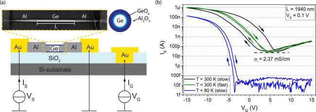
To investigate the electrical properties, VLS-grown Ge NWs with diameters of 30 nm were integrated in back-gated field-effect transistors (FETs). For device fabrication, a thermally induced exchange reaction between the NWs and Al contact pads is used to achieve Ge segments contacted by self-aligned, single-crystalline Al NW leads30 with atomically sharp heterojunctions (see Figure 1a).27 The particular monolithic and quasi-1D Al contact geometry prevents screening of the gate electric field, which is a common problem of nanoscale back-gated FETs with extended source/drain contacts.31 Details regarding the fabrication process as well as high-resolution transmission electron microscopy and energy dispersive X-ray spectroscopy investigations that prove the composition and perfect crystallinity of the NW heterostructure can be found in the work of Kral et al.27 and El Hajraoui et al.28 According to the large surface-to-volume ratio, adsorbates and surface states have significant impact on the electrical characteristics of NW-based devices.24,32 Consequently, to ensure reliable and reproducible electrical measurements, the NWs were enwrapped in a protective 20 nm thick ALD-grown Al2O3-shell (see schematic in Figure 1a).
Figure 1.
(a) Schematic and SEM image of an Al–Ge–Al NW heterostructure embedded in a back-gated FET architecture. The length and diameter of the actual NW are L = 1940 nm and d = 30 nm, respectively. A cross-section of the Ge channel enwrapped in a 20 nm Al2O3-shell is schematically shown in the upper right corner. (b) Transfer characteristics of a Ge NW FET device at a bias of VS = 0.1 V recorded at T = 300 K (black and green) and T = 80 K (blue) for gate voltage sweeping rates of 0.25 and 2.5 V/s, denoted slow and fast sweeping, respectively. The arrows indicate the gate voltage sweeping direction.
First, basic transfer characteristic measurements were conducted to determine the modulation capability of the charge-carrier type and concentration in the NWs. Figure 1b shows typical transfer characteristics of a FET device with a Ge channel length of L = 1940 nm recorded with a rather slow gate voltage sweeping rate of 0.25 V/s at T = 300 K (black) and 80 K (blue).
At room temperature, the nominally intrinsic Ge NW exhibits ambipolar behavior, with hole accumulation at negative gate voltages and moderate inversion at VG > 7 V, which is commonly observed for intrinsic semiconductor NWs.14 Surface doping,33 due to acceptor-like traps, results in a shift of the energy band structure throughout the whole NW, causing p-type behavior in nominally intrinsic Ge NWs.23,24 Furthermore, the transfer characteristic measured at T = 300 K reveals an ION/IOFF ratio of about 104 and distinct hysteresis effects.
In a simplified model (i.e., ohmic contacts and no
band bending
across the NW), one can assume that the conductivity at the minimum
of the transfer characteristic corresponds to the conductivity of
an intrinsic semiconductor (Fermi level at mid-gap) with the number
of free electrons and holes equal to the intrinsic carrier density ni. Using σ = e(nμn + pμp) and assuming simplified equal mobilities of
electrons and holes, the average carrier mobility in the channel can
be calculated according to  . For the actual device with σi = 2.37 mS/cm, the calculated value of μ
= 370 cm2/(V s), which is in good agreement with a former
work on similar Ge NWs.24 The overall lower
mobility compared to bulk Ge is mainly attributed to pronounced surface
scattering in thin NWs.34,35
Furthermore, we observed a pronounced hysteresis with the current to be not only dependent on VG but also the gate voltage sweeping direction and rate affecting the population of trap states in different ways.23 The surface of Ge NWs with typical interface trap densities of 1013–1014 /(eV cm2),24 up to three orders of magnitude higher compared to planar Ge structures, corresponding to roughly 0.2–2% of the surface atoms,36 provide a large reservoir of such trap states, which act as a highly efficient local gate.18 Considering the Ge NW device shown in Figure 1a, a maximum of 20 000 traps are involved in determining the device behavior. With time constants in the range from microseconds to several minutes for interface and oxide states respectively,37 one cannot avoid hysteresis effects for dynamic measurements of Ge NW FETs.14 However, as exemplarily shown in Figure 1b, upon increasing the sweeping rate from 0.25 V/s (black) to 2.5 V/s (green), the hysteresis is significantly reduced. As the trapping and detrapping of electrons is a kinetically limited process,23 the time constants significantly increase at lower temperatures. Thus, measuring the transfer characteristic with a slow gate voltage sweeping rate of 0.25 V/s but at T = 80 K, leads also to a notable reduction of the hysteresis (blue curve in Figure 1b). The remarkable high ION/IOFF ratio of 107 is a result of the steeper Fermi distribution at lower temperatures,4 and as shown below an overall reduced shielding of the electrostatic gate by the traps.
Figure 2 shows the transient response of the Ge NW device at room temperature and T = 80 K when the gate voltage is abruptly switched from VG = −15 to 15 V. At room temperature and a gate voltage of VG = −15 V, a moderate bias voltage of VS = 0.1 V induces an instantaneous hole-dominated current of about IS = 400 nA (t = 0 min). Over a timespan of more than 60 min, the current decreases continuously by about 4 orders of magnitude, approaching a steady-state value of approximately 10 pA. At this point (t = 70 min), the gate voltage is abruptly switched to VG = 15 V, which according to the transfer characteristic in Figure 1, causes a polarity change and a sudden current increase to IS = 200 pA. This electron-driven current progresses nonmonotonically over time, with the minimum lower than the steady state at VG = −15 V.
Figure 2.
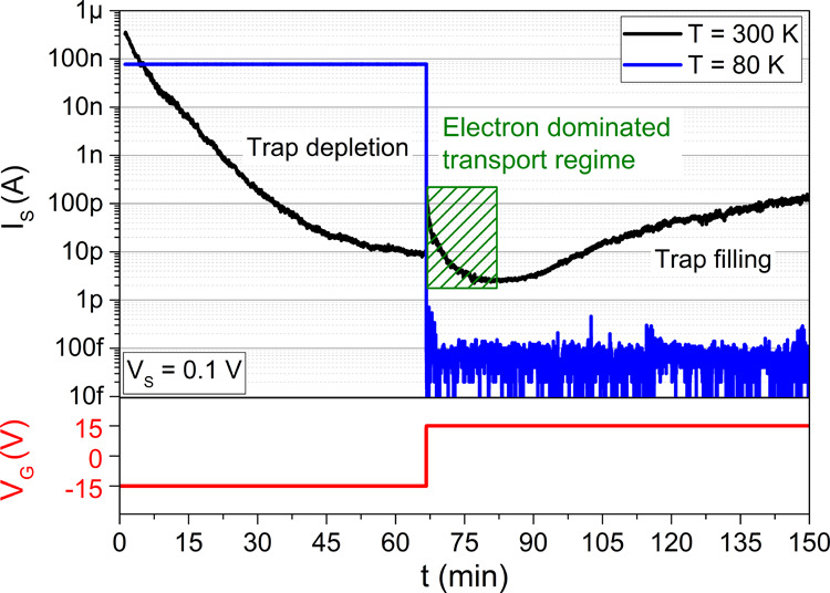
Transient response of a Ge NW FET device for a fixed bias voltage of VS = 0.1 V and abrupt changes in the gate voltage measured at T = 300 K (black) and T = 80 K (blue). The green shaded region marks the electron-dominated transport regime. The length and diameter of the actual NW is L = 920 nm and d = 30 nm, respectively.
In contrast, if the same measurement is conducted at T = 80 K, no such transient behavior was observed. A negative gate voltage of VG = −15 V provokes an instantaneous current of IS = 78 nA (t = 0 min), which remains perfectly stable over time. The abrupt switching of the gate voltage to VG = 15 V (t = 70 min) results in an immediate drop of IS below the noise level of our measurement setup.
To explain the progress of IS over time, a model is proposed in which the transient behavior results from the gate-controlled redistribution of charged surface traps. The schematics in Figure 3 illustrates the combined effects of the gate voltage and thereof controlled surface trap population on the band structure of an intrinsic Ge NW. At VG = 0 V and under equilibrium conditions, the low energetic traps below the Fermi level are filled up with electrons, while those above remain empty. (i) These charged traps close to the FET channel act as an effective negative gate (further denoted as local gate), inducing band bending and the common p-type behavior of nominally intrinsic Ge NWs.23,38 Upon applying a negative gate voltage, the Fermi level shifts towards the valence band, inducing instantaneous hole accumulation (ii) and thus an abrupt increase of IS as shown in Figure 2 at t = 0. According to the lowered Fermi level, filled traps start to be discharged and the local gate becomes less negative, resulting in reduced band bending. As the time constants of surface states in Ge can be extremely long,37 the current decreases continuously for more than 60 min before a steady state (iii) is reached. In contrast, by applying a positive gate voltage of VG = 15 V, the Fermi level shifts towards the conduction band inducing channel inversion i.e., electron-dominated transport at the surface (iv). As there are now empty traps below the Fermi energy, they start filling up with electrons and the local gate becomes more negative counteracting the positive back gate. This continues until an equilibrium is reached and a similar band bending to that for VG = 0 V is obtained, but now with a higher number of filled traps (v). This very effective negative local gate overcompensates the positive back gate and after a short period of electron-dominated transport, marked by the green dashed area in Figure 2, the mechanism changes back to hole-dominated electrical transport.
Figure 3.
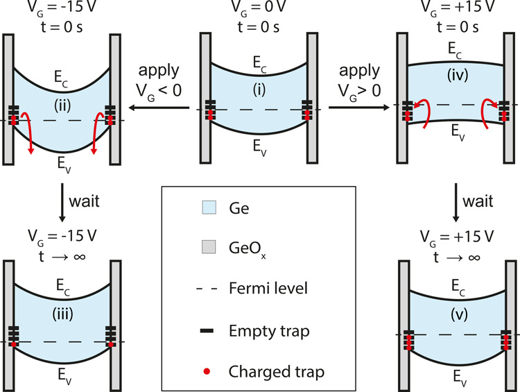
Cross-sectional band structure of a Ge NW device to illustrate the transient behavior of the gate-controlled redistribution of charged surface traps: (i) Ge NW at VG = 0 V in equilibrium. (ii) Applying a negative gate voltage lowers the Fermi level, which results in the discharging of the surface traps. (iii) Equilibrium is reached with VG = −15 V and fewer traps are filled. (iv) Applying a positive gate voltage lifts the Fermi level and results in downward band bending and thus inversion at the surface. (v) The continuous filling of traps causes the NW to reach equilibrium again with a higher number of traps filled.
The ability to change the polarity of current transport via electronic surface doping will now be strikingly demonstrated by inducing NDR in the Ge NW device. For common n-doped Ge, NDR can be explained by the transferred electron effect following the Ridley–Watkins–Hilsum theory.39 At sufficiently high electric fields, electrons from the energetically favorable conduction band valley, characterized by a low effective mass, are transferred to a heavy mass valley nearby.40 Although the Γ-point minimum in Ge is energetically closer to the L-point minimum, the coupling constant between ⟨111⟩ and ⟨000⟩ minima is significantly lower than that between ⟨111⟩ and ⟨100⟩ minima.41 Consequently, as schematically illustrated in the inset of Figure 4a, the transferred electron effect in Ge applies for the L-point and Δ-point minima of the ⟨111⟩ and ⟨100⟩ subbands of the conduction band with the respective effective masses of m*L,t = 0.082m0 and m*Δ,t = 0.288m0.
Figure 4.
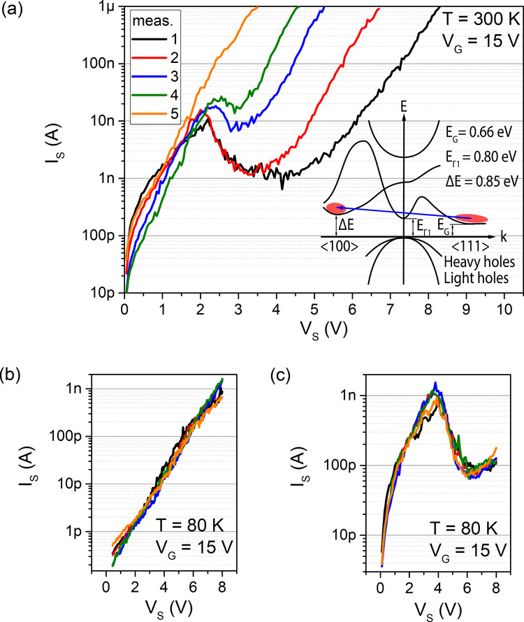
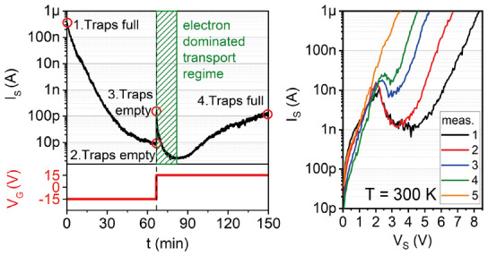
I/V curves of the Ge NW device with L = 920 nm and d = 30 nm measured at VG = 15 V in intervals of 1 min. Prior to the measurements, the traps were depleted at VG = −15 V for 60 min. (a) At T = 300 K, clear indications of NDR are visible during the first 4 measurements where the predominant transport mechanism is n-type. After about 5 min, when the polarity has changed back to hole-dominated electrical transport, the NDR effect disappears completely. The inset shows the band diagram of Ge with the electric field induced electron transfer from the ⟨111⟩ valley into the ⟨100⟩ valley. The polarity can be conserved by cooling down the previously depleted Ge NW device for 60 min at VG = −15 V. (b) Upon abruptly switching the gate voltage at T = 80 K to VG = 15 V, the device remains in the hole-driven transport regime resulting in a linear I/V characteristic. (c) After the initial trap depletion procedure (VG = −15 V for 60 min), the device was cooled down to T = 150 K and the gate voltage was abruptly changed to VG = 15 V to initiate n-type behavior. A subsequent cooldown to T = 80 K conserved the electron-dominated transport.
To induce NDR in the intrinsic Ge NWs, we forced the device into the electron-dominated transport regime (green shaded area in Figure 2). After depleting the traps at VG = −15 V for 60 min, the gate was switched to VG = 15 V and I/V characteristics were measured in intervals of 1 min (Figure 4a). For the first measurement, where a high electron density in the inverted channel dominates the transport, unambiguous signatures of NDR were observed with a maximum peak-to-valley ratio (PVR) of about 10. For the successive measurements, the PVR decreases gradually as traps are continuously filled and thus less electrons contribute to the transport in the channel. Finally, after about 5 min, when the polarity is changed back to hole-dominated electrical transport, the NDR effect disappears completely.
As already demonstrated, at T = 80 K, a redistribution of traps by the means of electrostatic gating is kinetically blocked.18,23 Consequently, it should be possible to freeze-in the transport regime based on the polarity of the device set at room temperature. Thus, by cooling down the Ge NW device, which was previously depleted for 60 min at VG = −15 V, one can conserve the polarity. Thus, when the gate voltage at T = 80 K is abruptly switched to VG = 15 V, the device remains in the hole-driven transport regime, resulting in the linear I/V characteristic shown in Figure 4b.
Setting up a stable electron-dominated transport required a slightly more complex process. After the initial trap depletion procedure (VG = – 15 V for 60 min), the device was cooled down to T = 150 K, where it was still possible to induce redistribution of traps by electrostatic gating. Next, the gate voltage was abruptly changed to VG = 15 V to initiate n-type behavior (green shaded area of Figure 2). Subsequently, the device was cooled down to T = 80 K as quickly as possible freezing-in the electron-dominated transport. In contrast to the room temperature measurements shown in Figure 4a, it was now possible to reproducibly measure a stable NDR over minutes with a constant PVR of 21 (see Figure 4c).
Finally, we want to stress once again that both a large number of surface traps due to the large surface-to-volume ratio as well as contact issues common for nanoscale structures are among the most severe issues of Ge NW-based devices. Hence, a combination of a protective Al2O3-shell and reliable single-crystalline Al contacts was required to enable systematic analysis of the complex transient behavior of Ge NWs. Our findings are based on the evaluation of the electrical data of more than ten similar passivated Al–Ge–Al NW heterostructure devices. Beside some minor device-to-device variations, we qualitatively found the same behavior for all investigated Ge NW-based devices.
Conclusions
We have thoroughly analyzed the influence of surface trap states on the electrical transport properties of intrinsic Ge NW. Controlling the trap population by electrostatic gating, we demonstrated the potential of effective surface doping to cause a transition of charge transport from hole- to electron-driven, enabling NDR in intrinsic Ge. Importantly, the electrostatic control of surface states may enable to avoid the charge trapping related hysteresis effect that is commonly considered parasitic for nanoelectronics and even introduces new functionalities based on polarity control. Consequently, our investigations provide a framework for utilizing surface trapping related transport phenomena in Ge nanostructures, which could be a significant step towards the development of future device concepts for post-Si nanoelectronic and nanophotonic devices.
Acknowledgments
The authors gratefully acknowledge financial support by the Austrian Science Fund (FWF): Project No.: P29729-N27. The authors further thank the Center for Micro- and Nanostructures for providing the cleanroom facilities.
Author Contributions
M.S. and P.S. contributed equally to this work. P.S. and M.S. performed the device fabrication, conducted the measurements, and wrote the manuscript. A.L. conceived the project and contributed essentially to the experimental design. All authors analyzed the results and helped shape the research and manuscript.
The authors declare no competing financial interest.
References
- Moore G. E. Cramming More Components onto Integrated Circuits. IEEE Solid-State Circuits Soc. Newslett. 2006, 11, 33–35. 10.1109/N-SSC.2006.4785860. [DOI] [Google Scholar]
- Chau R.; Doyle B.; Datta S.; Kavalieros J.; Zhang K. Integrated Nanoelectronics for the Future. Nat. Mater. 2007, 6, 810–812. 10.1038/nmat2014. [DOI] [PubMed] [Google Scholar]
- Thompson S. E.; Parthasarathy S. Moore’s Law: The Future of Si Microelectronics. Mater. Today 2006, 9, 20–25. 10.1016/S1369-7021(06)71539-5. [DOI] [Google Scholar]
- Sze S. M.; NG K. K.. Physics of Semiconductor Devices; John Wiley & Sons, Inc.: New Jersey, 2006. [Google Scholar]
- Gu G.; Burghard M.; Kim G. T.; Düsberg G. S.; Chiu P. W.; Krstic V.; Roth S.; Han W. Q. Growth and Electrical Transport of Germanium Nanowires. J. Appl. Phys. 2001, 90, 5747–5751. 10.1063/1.1413495. [DOI] [Google Scholar]
- Bruno M.; Palummo M.; Marini A.; Del Sole R.; Olevano V.; Kholod A. N.; Ossicini S. Excitons in Germanium Nanowires: Quantum Confinement, Orientation, and Anisotropy Effects within a First-Principles Approach. Phys. Rev. B: Condens. Matter Mater. Phys. 2005, 72, 153310 10.1103/PhysRevB.72.153310. [DOI] [Google Scholar]
- Johansson J.; Dick K. A. Recent Advances in Semiconductor Nanowire Heterostructures. CrystEngComm 2011, 13, 7175. 10.1039/c1ce05821e. [DOI] [Google Scholar]
- Brunco D. P.; De Jaeger B.; Eneman G.; Satta A.; Terzieva V.; Souriau L.; Leys F. E.; Pourtois G.; Houssa M.; Opsomer K.; et al. Germanium: The Past and Possibly a Future Material for Microelectronics. ECS Trans. 2007, 11, 479–493. 10.1149/1.2779584. [DOI] [Google Scholar]
- Claeys C.; Simoen E.. Germanium Based Technologies—From Materials to Devices; Elsevier B.V.: Oxford, U.K., 2007. [Google Scholar]
- Rastogi P.; Dutta T.; Kumar S.; Agarwal A.; Chauhan Y. S. Quantum Confinement Effects in Extremely Thin Body Germanium N-MOSFETs. IEEE Trans. Electron Devices 2015, 62, 3575–3580. 10.1109/TED.2015.2477471. [DOI] [Google Scholar]
- Xia Z.; Song H.; Kim M.; Zhou M.; Chang T.-H.; Liu D.; Yin X.; Xiong K.; Mi H.; Wang X.; et al. Single-Crystalline Germanium Nanomembrane Photodetectors on Foreign Nanocavities. Sci. Adv. 2017, 3, e1602783 10.1126/sciadv.1602783. [DOI] [PMC free article] [PubMed] [Google Scholar]
- Wagner R. S.; Ellis W. C. Vapor-Liquid-Solid Mechanism of Single Crystal Growth. Appl. Phys. Lett. 1964, 4, 89–90. 10.1063/1.1753975. [DOI] [Google Scholar]
- Gu G. G.; Burghard M.; Kim G. T.; Düsberg G. S.; Chiu P. W.; Krstic V.; Roth S.; Han W. Q. Growth and Electrical Transport of Germanium Nanowires. J. Appl. Phys. 2001, 90, 5747–5751. 10.1063/1.1413495. [DOI] [Google Scholar]
- Wang D.; Chang Y.-L.; Wang Q.; Cao J.; Farmer D. B.; Gordon R. G.; Dai H. Surface Chemistry and Electrical Properties of Germanium Nanowires. J. Am. Chem. Soc. 2004, 126, 11602–11611. 10.1021/ja047435x. [DOI] [PubMed] [Google Scholar]
- Heinzig A.; Slesazeck S.; Kreupl F.; Mikolajick T.; Weber W. M. Reconfigurable Silicon Nanowire Transistors. Nano Lett. 2012, 12, 119–124. 10.1021/nl203094h. [DOI] [PubMed] [Google Scholar]
- Jia C.; Lin Z.; Huang Y.; Duan X. Nanowire Electronics: From Nanoscale to Macroscale. Chem. Rev. 2019, 119, 9074–9135. 10.1021/acs.chemrev.9b00164. [DOI] [PubMed] [Google Scholar]
- Kim C.-J.; Lee H.-S.; Cho Y.-J.; Kang K.; Jo M.-H. Diameter-Dependent Internal Gain in Ohmic Ge Nanowire Photodetectors. Nano Lett. 2010, 10, 2043–2048. 10.1021/nl100136b. [DOI] [PubMed] [Google Scholar]
- Staudinger P.; Sistani M.; Greil J.; Bertagnolli E.; Lugstein A. Ultrascaled Germanium Nanowires for Highly Sensitive Photodetection at the Quantum Ballistic Limit. Nano Lett. 2018, 18, 5030–5035. 10.1021/acs.nanolett.8b01845. [DOI] [PubMed] [Google Scholar]
- Fadaly E. M. T.; Dijkstra A.; Suckert J. R.; Ziss D.; van Tilburg M. A. J.; Mao C.; Ren Y.; van Lange V. T.; Korzun K.; Kölling S.; et al. Direct-Bandgap Emission from Hexagonal Ge and SiGe Alloys. Nature 2020, 580, 205–209. 10.1038/s41586-020-2150-y. [DOI] [PubMed] [Google Scholar]
- Nikoobakht B. Toward Industrial-Scale Fabrication of Nanowire-Based Devices. Chem. Mater. 2007, 19, 5279–5284. 10.1021/cm071798p. [DOI] [Google Scholar]
- Singh N.; Buddharaju K. D.; Manhas S. K.; Agarwal A.; Rustagi S. C.; Lo G. Q.; Balasubramanian N.; Kwong D.-L. Si, SiGe Nanowire Devices by Top–Down Technology and Their Applications. IEEE Trans. Electron Devices 2008, 55, 3107–3118. 10.1109/TED.2008.2005154. [DOI] [Google Scholar]
- Lu W.; Lieber C. M. Nanoelectronics from the Bottom Up. Nat. Mater. 2007, 6, 841–850. 10.1038/nmat2028. [DOI] [PubMed] [Google Scholar]
- Hanrath T.; Korgel B. A. Influence of Surface States on Electron Transport through Intrinsic Ge Nanowires. J. Phys. Chem. B 2005, 109, 5518–5524. 10.1021/jp044491b. [DOI] [PubMed] [Google Scholar]
- Zhang S.; Hemesath E. R.; Perea D. E.; Wijaya E.; Lensch-Falk J. L.; Lauhon L. J. Relative Influence of Surface States and Bulk Impurities on the Electrical Properties of Ge Nanowires. Nano Lett. 2009, 9, 3268–3274. 10.1021/nl901548u. [DOI] [PubMed] [Google Scholar]
- Berger P. R.; Ramesh A.. Negative Differential Resistance Devices and Circuits; Elsevier BV.: Amsterdam, Netherlands, 2011. [Google Scholar]
- Sistani M.; Bartmann M. G.; Güsken N. A.; Oulton R. F.; Keshmiri H.; Luong M. A.; Momtaz Z. S.; Den Hertog M. I.; Lugstein A. Plasmon-Driven Hot Electron Transfer at Atomically Sharp Metal–Semiconductor Nanojunctions. ACS Photonics 2020, 7, 1642–1648. 10.1021/acsphotonics.0c00557. [DOI] [PMC free article] [PubMed] [Google Scholar]
- Kral S.; Zeiner C.; Stöger-Pollach M.; Bertagnolli E.; den Hertog M. I.; Lopez-Haro M.; Robin E.; El Hajraoui K.; Lugstein A. Abrupt Schottky Junctions in Al/Ge Nanowire Heterostructures. Nano Lett. 2015, 15, 4783–4787. 10.1021/acs.nanolett.5b01748. [DOI] [PMC free article] [PubMed] [Google Scholar]
- El Hajraoui K.; Luong M. A.; Robin E.; Brunbauer F.; Zeiner C.; Lugstein A.; Gentile P.; Rouvière J.-L.; Den Hertog M. In Situ Transmission Electron Microscopy Analysis of Aluminum–Germanium Nanowire Solid-State Reaction. Nano Lett. 2019, 19, 2897–2904. 10.1021/acs.nanolett.8b05171. [DOI] [PMC free article] [PubMed] [Google Scholar]
- Sistani M.; Staudinger P.; Greil J.; Holzbauer M.; Detz H.; Bertagnolli E.; Lugstein A. Room-Temperature Quantum Ballistic Transport in Monolithic Ultrascaled Al–Ge–Al Nanowire Heterostructures. Nano Lett. 2017, 17, 4556–4561. 10.1021/acs.nanolett.7b00425. [DOI] [PMC free article] [PubMed] [Google Scholar]
- Brunbauer F. M.; Bertagnolli E.; Majer J.; Lugstein A. Electrical Transport Properties of Single-Crystal Al Nanowires. Nanotechnology 2016, 27, 385704 10.1088/0957-4484/27/38/385704. [DOI] [PubMed] [Google Scholar]
- Neophytou N.; Guo Jing.; Lundstrom M. S. Three-Dimensional Electrostatic Effects of Carbon Nanotube Transistors. IEEE Trans. Nanotechnol. 2006, 5, 385–392. 10.1109/TNANO.2006.876912. [DOI] [Google Scholar]
- Winkler K.; Bertagnolli E.; Lugstein A. Origin of Anomalous Piezoresistive Effects in VLS Grown Si Nanowires. Nano Lett. 2015, 15, 1780–1785. 10.1021/nl5044743. [DOI] [PMC free article] [PubMed] [Google Scholar]
- Greytak A. B.; Lauhon L. J.; Gudiksen M. S.; Lieber C. M. Growth and Transport Properties of Complementary Germanium Nanowire Field-Effect Transistors. Appl. Phys. Lett. 2004, 84, 4176–4178. 10.1063/1.1755846. [DOI] [Google Scholar]
- Tahini H.; Chroneos A.; Grimes R. W.; Schwingenschlögl U.; Dimoulas A. Strain-Induced Changes to the Electronic Structure of Germanium. J. Phys.: Condens. Matter 2012, 24, 195802 10.1088/0953-8984/24/19/195802. [DOI] [PubMed] [Google Scholar]
- Pillarisetty R. Academic and Industry Research Progress in Germanium Nanodevices. Nature 2011, 479, 324–328. 10.1038/nature10678. [DOI] [PubMed] [Google Scholar]
- Statz H.; DeMars G. A.; Davis L.; Adams A. Surface States on Silicon and Germanium Surfaces. Phys. Rev. 1956, 101, 1272–1281. 10.1103/PhysRev.101.1272. [DOI] [Google Scholar]
- Kingston R. H. Review of Germanium Surface Phenomena. J. Appl. Phys. 1956, 27, 101–114. 10.1063/1.1722317. [DOI] [Google Scholar]
- Zhang Z.; Yates J. T. Band Bending in Semiconductors: Chemical and Physical Consequences at Surfaces and Interfaces. Chem. Rev. 2012, 112, 5520–5551. 10.1021/cr3000626. [DOI] [PubMed] [Google Scholar]
- Ridley B. K.; Watkins T. B. The Possibility of Negative Resistance Effects in Semiconductors. Proc. Phys. Soc. 1961, 78, 293–304. 10.1088/0370-1328/78/2/315. [DOI] [Google Scholar]
- Butcher P. N. The Gunn Effect. Rep. Prog. Phys. 1967, 30, 303 10.1088/0034-4885/30/1/303. [DOI] [Google Scholar]
- Jacoboni C.; Nava F.; Canali C.; Ottaviani G. Electron Drift Velocity and Diffusivity in Germanium. Phys. Rev. B: Condens. Matter Mater. Phys. 1981, 24, 1014–1026. 10.1103/PhysRevB.24.1014. [DOI] [Google Scholar]


