Abstract
In this paper, we present the design and preliminary performance evaluation of a novel external multi-channel readout circuitry for small-pixel room-temperature semiconductor detectors, namely CdZnTe (CZT) and CdTe, that provide an excellent intrinsic spatial (250 and 500 μm pixel size) and an ultrahigh energy resolution (~1% at 122 keV) for X-ray and gamma-ray imaging applications. An analog front-end printed circuit board (PCB) was designed and developed for data digitization, data transfer and ASIC control of pixelated CZT or CdTe detectors. Each detector unit is 2 cm × 2 cm in size and 1 or 2 mm in thickness, being bump-bonded onto a HEXITEC ASIC, and wire-bonded to a readout detector module PCB. The detectors’ front-end is then connected, through flexible cables of up to 10 m in length, to a remote data acquisition system that interfaces with a PC through USB3.0 connection.
We present the design and performance of a prototype multi-channel readout system that can read out up to 24 detector modules synchronously. Our experimental results demonstrated that the readout circuitry offers an ultrahigh spectral resolution (0.8 keV at 60 keV and 1.05 keV at 122 keV) with the Cd(Zn)Te/HEXITEC ASIC modules tested. This architecture was designed to allow easy expansion to accommodate a larger number of detector modules, and the flexibility of arranging the detector modules in a large and deformable detector array without degrading the excellent energy resolution.
Keywords: Gamma-ray, Detector Room-temperature semiconductor detector, Spectroscopic, Multi-channel readout circuitry, Analog front-end, Cd(Zn)Te
1. Introduction
There is a rising demand for high-resolution room-temperature solid-state detectors (RTSDs), especially CZT and CdTe detectors, in clinical and preclinical nuclear imaging applications [1]. CZT and CdTe have shown clear advantages in comparison to the conventional scintillator materials (e.g. NaI(Tl)), such as an enhanced energy resolution due to the direct conversion of gamma rays to charge carriers, a fine spatial resolution due to the pixelated structure in the application-specific integrated circuit (ASIC), and a satisfactory detection efficiency for gamma rays emitted by commonly used radioisotopes in the clinical practice [1,2]. Lastly, a compact form factor and lightweight camera compared to the cumbersome photomultiplier tubes (PMTs) suggest that RTSD-based imaging sensors will slowly replace scintillation detectors for high-resolution nuclear medical imaging. An alternative to RTSDs is represented by solid-state readout devices such as SiPM- and APD-based detectors, coupled with scintillators without the need of PMTs [3]. Those devices show a compact form factor comparable to Cd(Zn)Te-based detectors, but are outperformed in terms of energy and spatial resolution [4,5], providing a 10%–15% FWHM at 511 keV and 1–2 mm FWHM versus 1%–7% FWHM at 511 keV and 0.35–1 mm FWHM from CZT detectors [4].
Clinical single-photon emission computed tomography (SPECT) systems based on CZT technology are already being developed and commercially available [6–10]. These commercial successes indicate that, even if the cost of Cd(Zn)Te detectors is much higher, medical systems based on such detectors present an improved performance and, therefore, are an attractive and growing technology. On the other side, a massive research effort is addressed to advance the crystal growth and device fabrication process for CZT detectors, to make them more cost effective and widespread their use [11,12].
As the demand for SPECT systems with higher spatial resolution, energy resolution and sensitivity continues to rise, there is an increasing need to develop high-performance small-pixel CZT and CdTe detectors and corresponding high-speed readout electronics. These detectors should ideally provide an excellent energy resolution, precise measurement of the interaction positions, an adequate detection efficiency over a broad energy range from 20 keV to 600 keV, and a compact and flexible footprint.
The multi-channel readout circuitry reported here is based on the pre-existing High Energy X-ray Imaging Technology (HEXITEC) ASIC, developed by the Science and Technology Facilities Council’s (STFC) Rutherford Appleton Laboratory (RAL) [13,14]. The HEXITEC ASIC is 3-side buttable, with a functional area of 20 mm × 20 mm that accommodates an 80 × 80 array of readout channels with 250 μm × 250 μm pitch [15–17]. The ASIC could be connected to p-type Si, GaAs, CdTe or CZT detectors with matching pixel patterns and allows for a readout speed of up to ~9k frames per second [14]. The HEXITEC ASIC was designed with two user-selectable energy ranges of roughly 4–200 keV and 20–600 keV [18], respectively.
There have been several readout systems based on the HEXITEC ASIC developed for various applications, ranging from material science [19–21], homeland security [22], to astrophysics, solar spectroscopy [23,24], and medical imaging [15,25,26]. These are mainly single-module readout systems whose circuitry is able to control and acquire from only one detector module at time. In multi-detector medical imaging applications where many and closely packed detector modules are needed (from 10 s for preclinical applications to 100 s for clinical ones), these external readout electronics are not suited or optimized in terms of packaging, compactness, power consumption, cooling and usage of common resources, and, therefore, are not cost-effective. The need of a multi-channel external readout electronics that preserves the performance of the single detector module is stated in [27].
The multi-channel readout system reported in this paper is partially motivated by our current development of two preclinical imaging systems: the first is the second-generation of a MR(magnetic resonance)-compatible SPECT system, which is referred to as MRC-SPECT-II system [28,29], based on 24 CZT/HEXITEC ASIC detector modules. The second development consists of a partial ring for X-ray fluorescence computed tomography (XFCT) applications [30,31]. The platform will be used for in vivo imaging of non-radioactive and metal-based therapeutic agents in small animals, such as gold, platinum and hafnium [32–34].
The primary goal of this work is to develop a compact, modular, and scalable readout circuitry based on the HEXITEC ASIC, which would offer a fine imaging resolution and an excellent spectroscopic performance over a broad energy range of 20–600 keV. The design architecture allows for easy expansion to detection systems with a large number of detector modules (e.g. 500 units anticipated for a clinical SPECT system). We have intentionally incorporated flexi-cables within the digital readout system to allow the physical detection system to take an arbitrary shape optimized for the given imaging application. This readout system would find its use in many applications, such as spectral SPECT and XFCT, which we referred to as hyperspectral single-photon imaging. To demonstrate its feasibility, we have developed and evaluated a prototype readout system that could be connected up to 24 Cd(Zn)Te/HEXITEC ASIC detector modules. The performance of the readout system was demonstrated with a CdTe/HEXITEC ASIC and a CZT/HEXITEC ASIC detector module connected to the readout system. Details of the prototype are discussed in the following sections and preliminary experimental results are presented.
2. Materials and methods
2.1. Cd(Zn)Te/HEXITEC ASIC detector modules
We have tested both CZT and CdTe detectors flip-chip bonded to the HEXITEC ASICs and then connected to the compact readout system described in this paper. The CdTe detector is 1 mm in thickness and is procured by Acrorad Co Ltd [35] and the CZT detector is 2 mm in thickness and is procured by Redlen (http://redlen.ca/). Both the CZT and CdTe detectors have an active area of 20 mm × 20 mm. The CdTe elements are Schottky-diode type with a large planar platinum cathode and a pixelated aluminum anode with 250 μm pitch (with individual metal contact of 200 μm × 200 μm in size and an inter-pixel gap of 50 μm). The CZT elements are ohmic type with a gold planar cathode and a gold pixelated 500 μm pitch (metal contact of 450 × 450 μm with an inter-pixel gap of 50 μm). Both the CdTe and CZT detectors were flip-chip-bonded to the HEXITEC readout ASIC using gold studs and silver epoxy [14,36,37]. All the specifications are summarized in Table 1.
Table 1.
Specifications of the RTSDs used.
| CdTe | CZT | |
|---|---|---|
| Manufacturer | Acrorad | Redlen |
| Type | Schottky-diode | Ohmic |
| Active Area | 20 mm × 20 mm | 20 mm × 20 mm |
| Thickness | 1 mm | 2 mm |
| Anode | Platinum | Gold |
| Cathode | Aluminum | Gold |
| Pixel array | 80 × 80 pixels | 40 × 40 pixels |
| Pixel size | 250 μm × 250 μm pitch | 500 μm × 500 μm pitch |
| Anode pad size | 200 μm × 200 μm | 450 μm × 450 μm |
| Inter-pixel size | 50 μm | 50 μm |
As shown in Fig. 1, each channel of the HEXITEC ASIC consists of a charge-sensitive preamplifier with a leakage current compensation circuit, a shaping amplifier, a 2nd order low pass filter, and a peak-track-and-hold circuit [13,38]. Finally, a rolling shutter readout system reads out the pixel array frame row by row (4 parallel chains of 20 pixels for each row) allowing a fast readout rate of ~9 k frames per second for the entire ASIC [13,16]. The HEXITEC ASIC therefore provides precise interaction position and energy deposition for each gamma-ray interaction. The single frames of raw data are then processed and converted into single-pixel energy spectra. The ASIC can operate in high (2–200 keV) and low (6–600 keV) gain mode depending on the switch in the branch with the 36 fF capacitor in Fig. 1, which extends the dynamic energy range of the detector. The Cd(Zn)Te/HEXITEC ASIC modules are then wire-bonded to a detector module PCB and mounted on an aluminum support. The wire-bonding pads of the ASIC, including the control signals, power feeds and output signals, are located on the non-buttable side, as shown in Fig. 2.
Fig. 1.
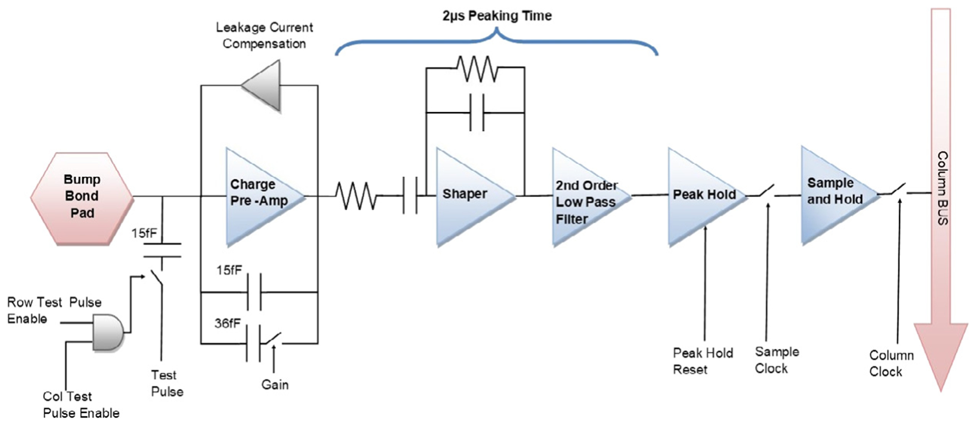
Block diagram of a single pixel electronics in a HEXITEC ASIC.
Fig. 2.
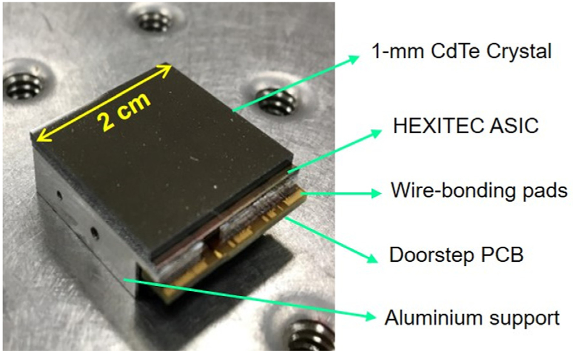
Single 1-mm-thick CdTe/HEXITEC ASIC module, 2 cm × 2 cm in size.
The intent to use two different types of detectors is based on application-specific imaging and spectroscopic requirements. The 1-mm-thick CdTe crystals have already shown superior energy resolution properties (1 keV at 140 keV [15]), which makes them well-suited for multi-isotope SPECT imaging or XFCT applications, while the 2-mm-thick CZT detector has an increased detection efficiency for gamma rays having energies >150 keV with slightly poorer spectral capabilities [36]. It is worth to note that the detection efficiency of 1-mm CdTe and 2-mm CZT at energies > 300 keV would be too low (9.50% and 18.09%, respectively), and thicker crystals are needed (≥ 5 mm). Based on this, a readout electronics with depth of interaction (DOI) capabilities is under development [39].
2.2. The multi-channel readout circuitry
The developed readout system for the multi-module CdTe/CZT detector system consists of two major parts. The front-end circuitry starts from two Cd(Zn)Te/HEXITEC ASIC detector modules connected to a custom-designed readout PCB (which will be referred to as the front-end PCB throughout this paper). It supplies HV bias and power, provides control logic, and digitalizes the amplified analog signals from the anode pixels. The front-end circuitry is then connected to a digital data acquisition (DAQ) system that allows direct streaming of all digitized pixel signal amplitudes to a mini PC through a USB3.0 interface. The front-end circuitry and the DAQ subsystem are connected through flexible cables of up to 10 meters in length. One of the emphases for the development of this readout system is to retain an ultrahigh energy resolution from the Cd(Zn)Te/HEXITEC ASIC detector modules [27]. The design of this readout system will be further detailed in the following sections.
2.2.1. Overall readout system design considerations
The main considerations for the proposed design are summarized below. First, due to the rising demand for high energy and spatial resolution applications in medical nuclear imaging, the new external readout electronics need to retain the ultra-high energy resolution provided by the small-pixel Cd(Zn)Te/HEXITEC ASIC detector modules.
Second, the readout system will be a reliable and high-speed platform able to manage data buffering and transferring of up to 1000 frames per second from 4 Cd(Zn)Te/HEXITEC ASIC detector modules simultaneously. Each detector module would allow to detect >100,000 events/cm2 per second, while maintaining excellent spatial and energy responses. The range of the detector widely satisfies count rates in clinical SPECT settings that are typically less than 50 kcps.
Third, the design would allow constructing an entire detection system based on multiple CZT or CdTe detector modules in a flexible and rearrangeable structure that can be easily tailored for different imaging applications, from the current preclinical MRC-SPECT-II and XFCT systems to future clinical imaging systems. The compact front-end PCB has reduced dimensions of 11.5 cm × 3.9 cm (Figs. 3–4) in comparison with the single-module HEXITEC PCB being 22 cm × 6 cm in size [14,37], and the flexi-cables used allow the detection system to take a shape optimized according to the imaging application. The modular and scalable design can be easily expanded adding one DAQ board and two front-end PCBs every 4 Cd(Zn)Te/HEXITEC ASIC modules. Common components and resources are more efficiently used for an overall compact and cost-effective geometry.
Fig. 3.
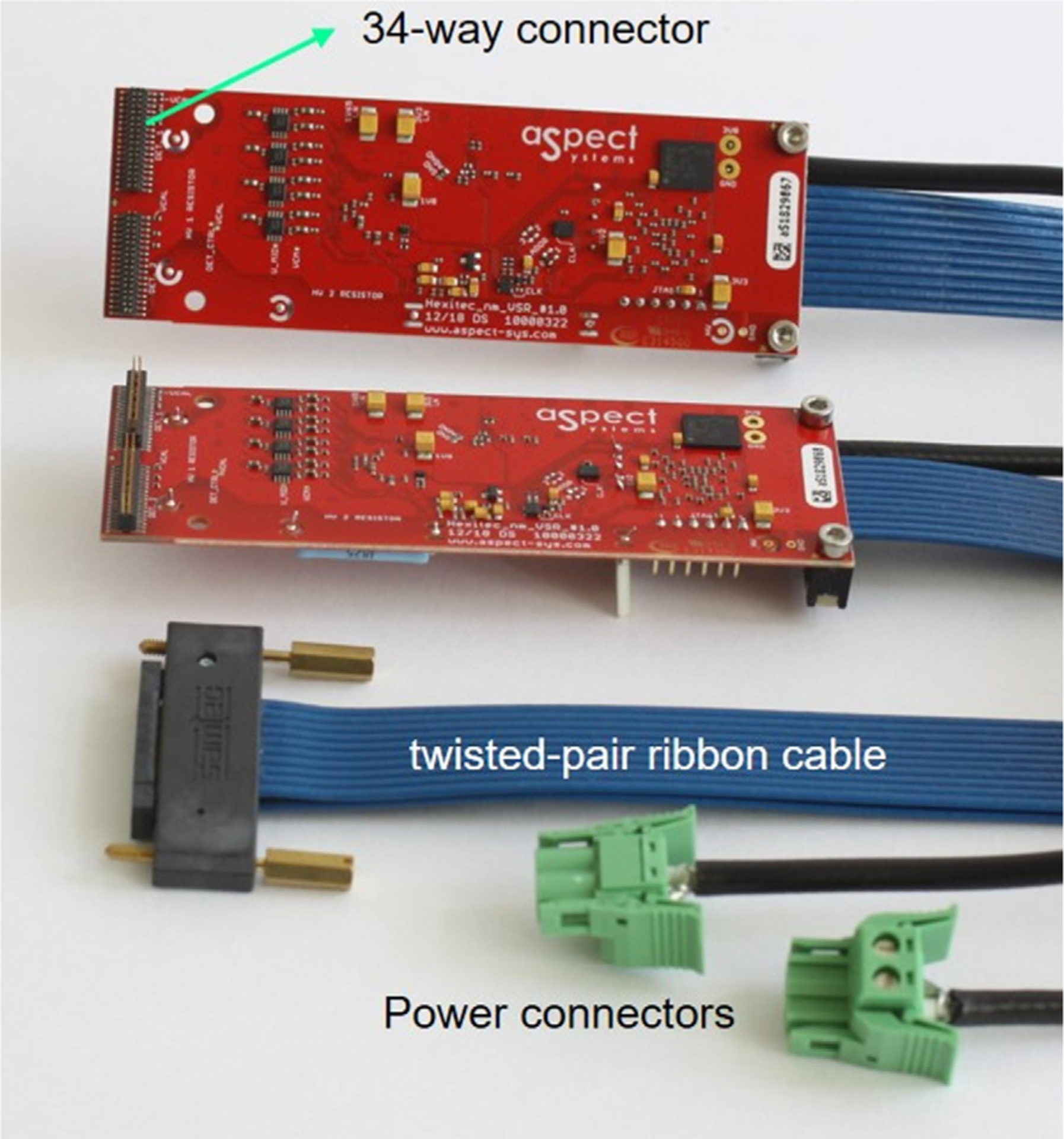
Two buffer analog front-end PCBs controlled by a single DAQ board, with power and data cables.
Fig. 4.
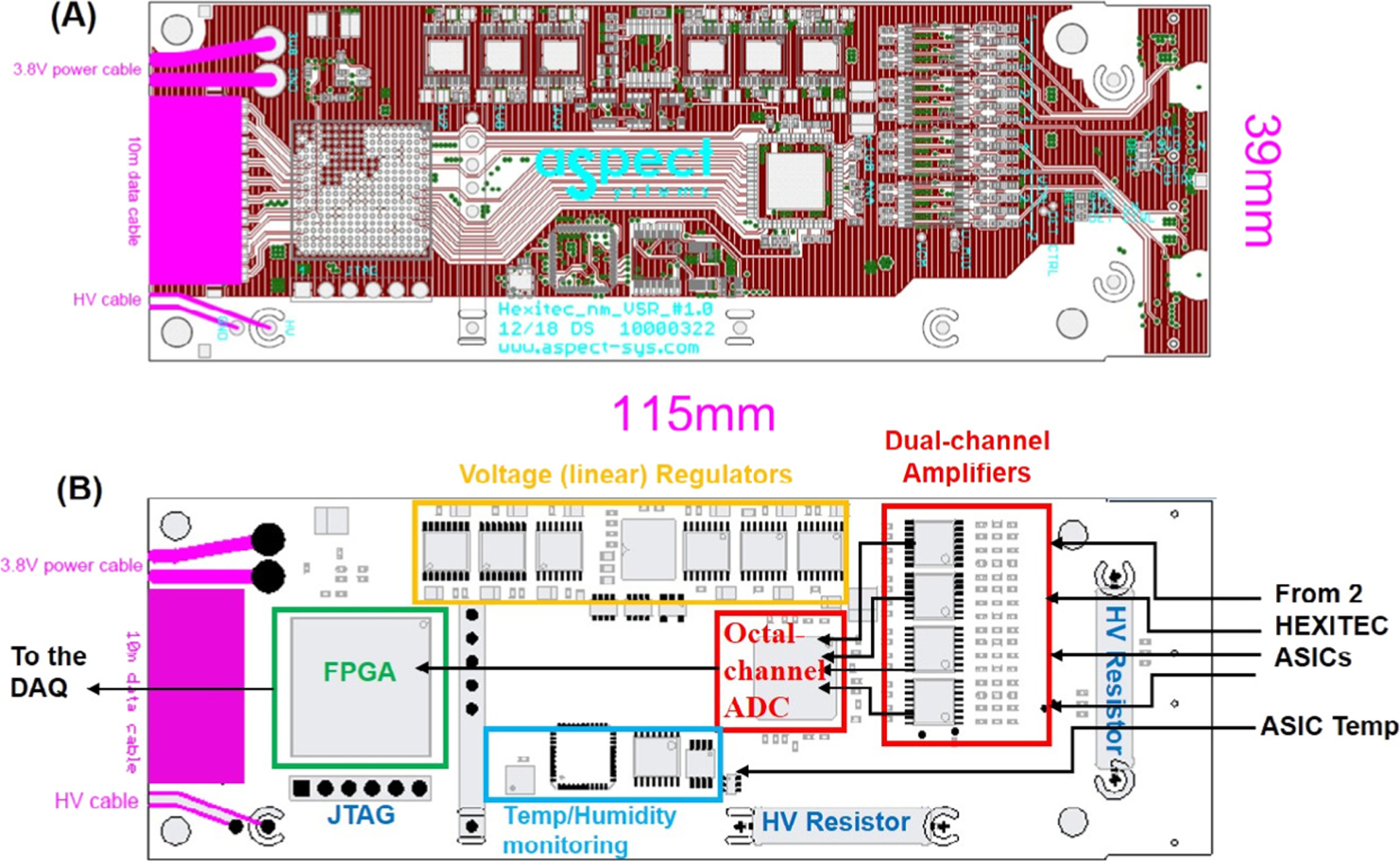
The analog front-end PCB: (A) the PCB layout and (B) the PCB functional block diagram.
2.2.2. Front-end electronics
The front-end readout circuitry is accommodate on the PCB as shown in Figs. 3–4. Each front-end PCB is connected to two CZT(or CdTe)/HEXITEC modules through two 34-way zero insertion force connectors (visible in Fig. 3). The block diagram of the front-end board is shown in Fig. 4B, which consists of the following functional blocks: (1) a digitization circuitry with four parallel very low-power, fully differential two-channel amplifiers and an eight-channel 14-bit ADC receives the multiplexed data from the two ASICs and digitalizes the peak-hold signal amplitude on each channel; (2) a field-programmable gate array (FPGA) that provides the 21.25 MHz clocks for the ASIC, controls the readout operation and the data transferring process between the front-end PCB and the remote DAQ system; (3) a voltage regulation circuitry receives the power supply (3.8 V) from a remote power supply unit and generates two power lines at 1.65 V and 3.3 V, respectively, to power each HEXITEC ASIC; and, finally, (4) an environmental monitoring circuitry that measures the temperature and humidity sensors on the PCB, measures the ASIC temperature from on an on-chip diode and feeds the readings to the FPGA and protecting logic to prevent the readout system from overheating. The high voltage bias, provided by the DAQ system or by an external power supply, is routed and decoupled on the front-end PCB, and it is connected to the CZT or CdTe sensors cathode via a wire bond. The signal from the FPGA acquired by two HEXITEC ASICs is then transmitted to a remote DAQ board through twisted-pair ribbon cables of up to 10 m in length as shown in Fig. 3.
2.2.3. Digital data acquisition (DAQ) System
The remote DAQ board (Fig. 5) is connected to two front-end PCBs, which reads out 4 HEXITEC ASICs synchronously. In the prototype mentioned in this study, 10-m long twisted-pair cables are used to connect the front-end PCBs to the remote DAQ board. The DAQ board provides the necessary cable interface, trigger inputs, and control logic to operate the two front-end PCBs connected.
Fig. 5.
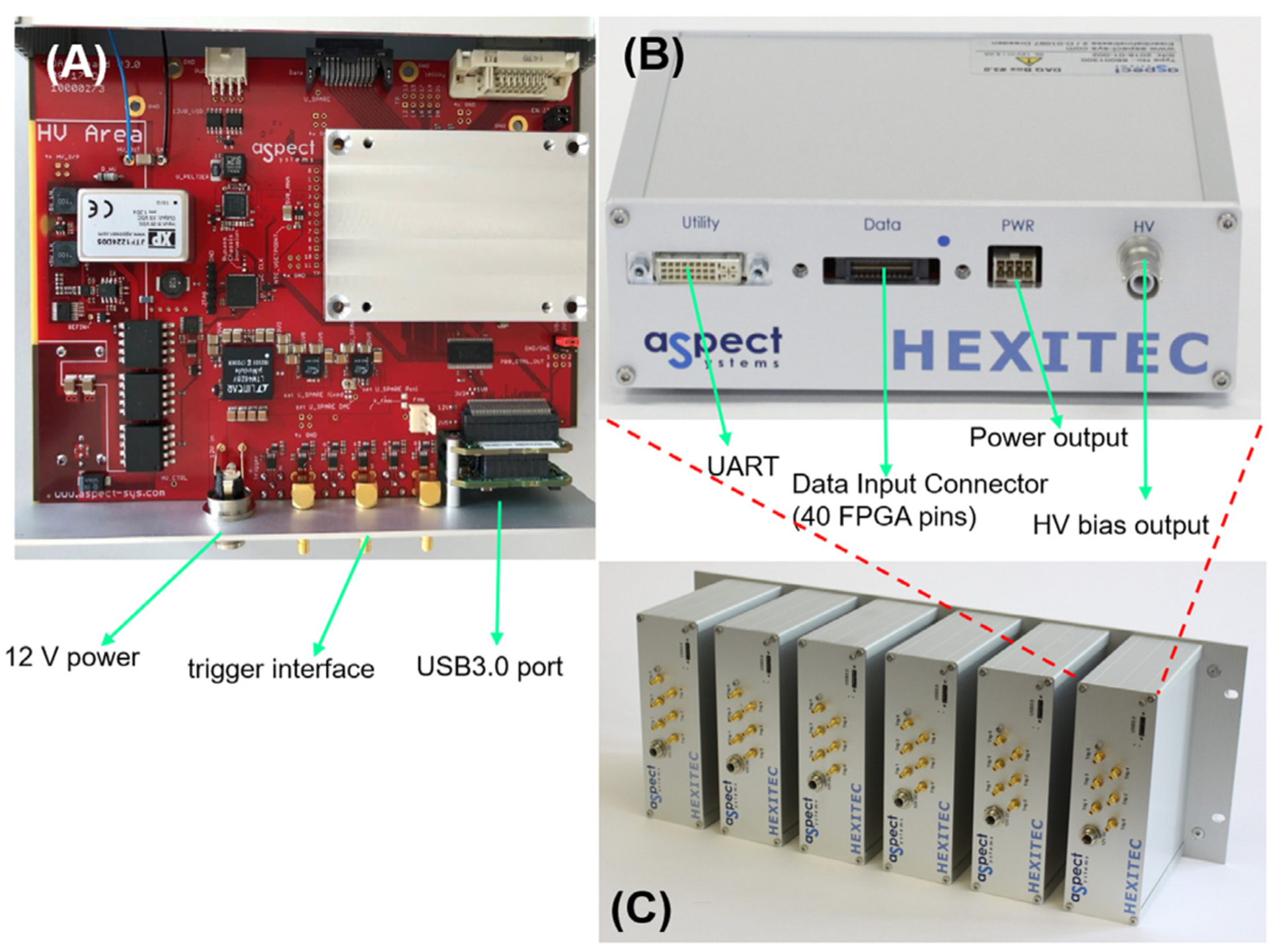
The remote DAQ board: (A) the physical board (B) single DAQ box (C) 6 DAQ boxes used in parallel in the final readout system.
The DAQ board contains an additional FPGA (Xilinx Zynq-7030), which captures the raw data from the analog front-end PCBs and locally formats the data for transmission via USB3.0 interface. The control interfaces, on the backside of the box (Fig. 5A), consist of a 12 V inlet for power, a USB 3.0 port for data output and a trigger interface. The applications interfaces available for the front-end PCBs on the front side of the DAQ box (Fig. 5B) are a Universal Asynchronous Receiver–Transmitter (UART), 40 FPGA pins for the input data transmitted through the twisted-pair ribbon cable according the Low-Voltage Differential Signaling (LVDS) standard, a power outlet that provides 12V/2A for powering the PCBs, a power outlet that provides 5V/6A and a PID circuit for powering and controlling the Peltier cooler units, and a power outlet for 0 to −750V HV bias supply.
A complete functional diagram is reported in Fig. 6 and presents the basic building block in the modular design. Each DAQ board is then connected to an Intel® NUC mini PC through USB-3 cable. Finally, the mini PCs are controlled by a control PC through Ethernet connection. The final readout circuitry consists of 12 analog front-end PCBs and 6 DAQ boards (Fig. 5C) to control synchronously up to 24 CZT/HEXITEC ASIC modules. The acquisition from each DAQ board is independent from the others and can be evaluated separately.
Fig. 6.
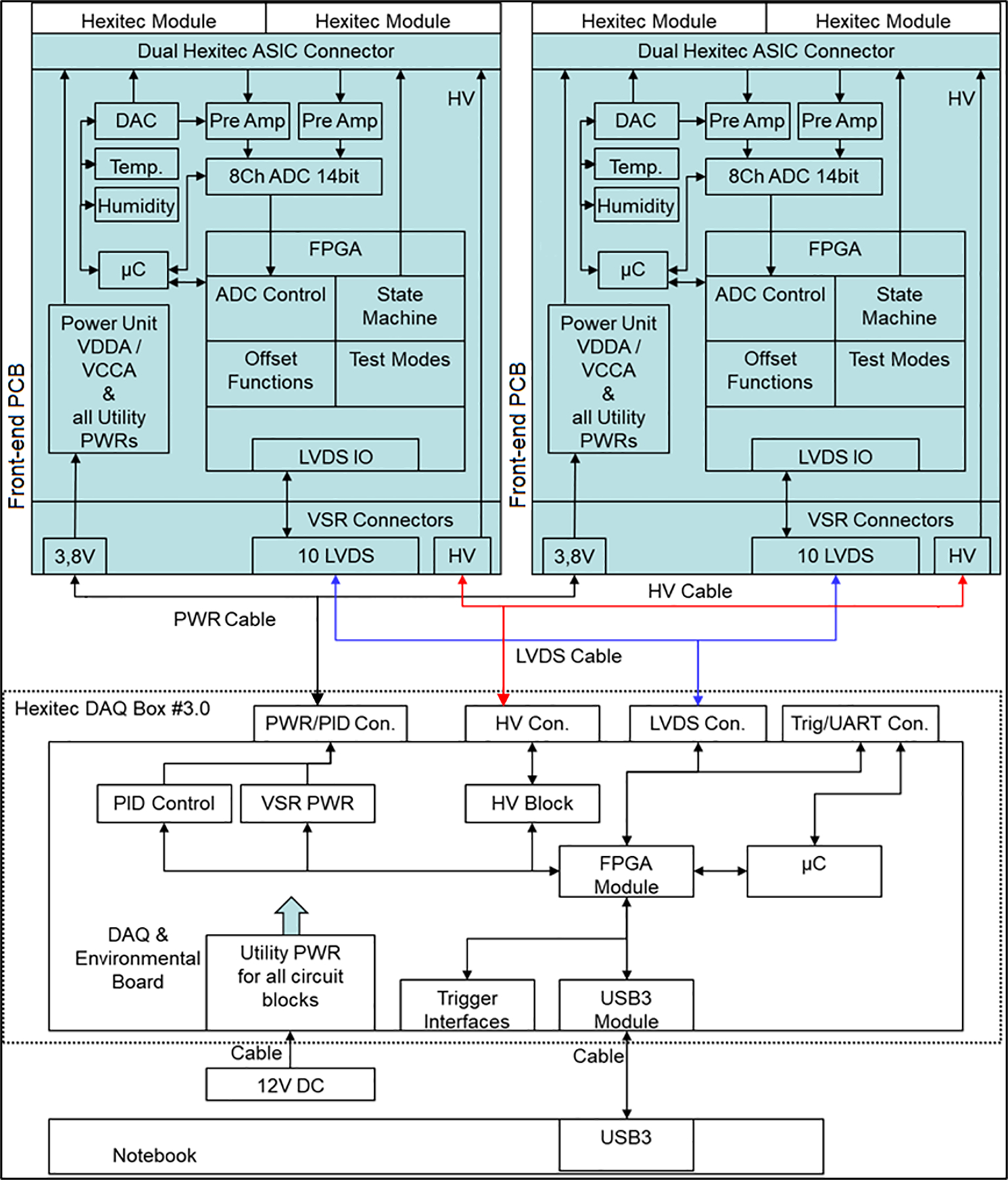
Complete functional block diagram of a single remote DAQ board (bottom) that controls and reads out two analog front-end PCBs (top) simultaneously.
2.2.4. Experimental evaluation with a detector module prototype
We have developed a 4-detector module setup that is connected to two front-end PCBs as shown in Fig. 7A and C. In this setup, a 2 × 2 array of CZT/HEXITEC detector hybrids are mounted on an aluminum substrate, leaving a physical gap of around 200 μm between adjacent detectors (less than one pixel). The aluminum substrate also supports two frond-end PCBs connected to the detector modules from two opposite sides. Two Peltier cooling units and a copper heat sink are used for cooling and heat dissipation, and a 3D-printed plastic support with inlets for compressed air completes the design (Fig. 7A). The power consumption of a single ASIC is around 1.5 W, while the maximum power consumption of two analog front-end PCBs and 4 Cd(Zn)Te/HEXITEC modules is 15.2 W.
Fig. 7.
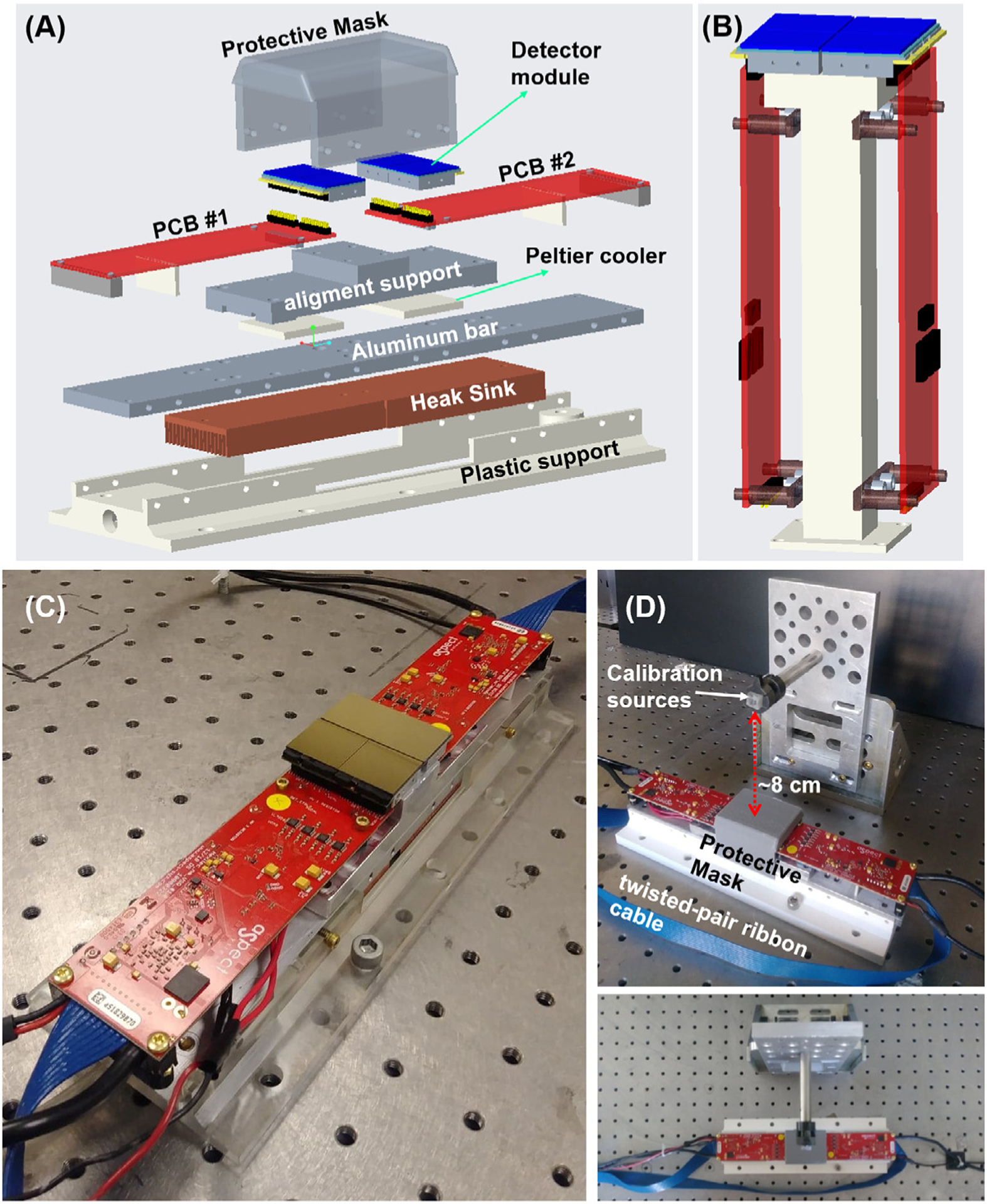
(A) 3D drawing (exploded view) of the compact testing setup with an aluminum substrate that holds 4 detectors connected to two analog front-end PCBs. (B) 3D drawing of the 2 × 2 array when 180° zero-force connectors between detector modules and analog front-end PCB are used. (C) Testing setup where four 1-mm-thick CZT detector modules are installed on the analog front-end PCBs connected to the corresponding DAQ board (D) Details of the experimental setup with top view.
It is worth to note that the 34-way zero insertion force connectors visible in Fig. 3 allow to mount the detector modules with the crystal surface parallel to the PCB surface (as shown in Fig. 7A and C), and the 2 × 2 arrays would be tiled only along one direction. To allow the tiling in both directions, 180° type connectors will be used, in order to have the crystal surface perpendicular to the PCB, as shown in Fig. 7B.
In order to evaluate the performance of the prototype readout electronics, a 1-mm-thick CdTe and a 2-mm-thick CZT detector were tested with the proposed prototype readout where the detector modules were installed on the analog front-end PCB connected to the corresponding DAQ board. The same settings and experimental conditions were used for both detector modules as described below and summarized in Table 2.
Table 2.
Specifications of the experimental setup.
| CdTe | CZT | |
|---|---|---|
| Sources | 0.029 mCi Co-57 (point source), | |
| 0.098 mCi Am-241 (disk source) | ||
| Distance | 8 cm | |
| Acquisition time | 120 min | |
| Acquisition rate | 500 fps | |
| HV bias voltage | −500 V | −600 V |
| HV bias refresh | Yes, 10 s every 2 min | No |
| Detector temperature | 24.8 °C | 23.9 °C |
A Co-57 point source of 0.029 mCi (photopeak at 122 keV and 136 keV) and Am-241 disk source of 0.098 mCi (photopeak at 59.5 keV) were used to irradiate the detector for 120 min from a distance of ~8 cm to ensure flat-field irradiation across the entire sensor (Fig. 7D). During the acquisition time, sufficient counts were detected in order to examine the single-pixel spectra. A bias voltage of −500 V was applied across the 1-mm-thick CdTe detector while −600V was used for the 2-mm-thick CZT. The polarization phenomenon happening in CdTe crystals is well known in literature [40,41], and switching the bias voltage off for a short period allows the polarized detector to return to its normal state [42]. Based on this, the high bias voltage on the 1-mm-thick CdTe detector was refreshed for 10 s every 2 min.
For each acquisition, the energy range selected is the 4–200 keV range and the acquisition rate was 500 frames per second. This acquisition rate ensured that independent photons were not detected by adjacent pixels in the same frame and allowed performing off-line change-sharing corrections. The CZT/CdTe detectors were operated at room temperature, however, because of the heat generated by the ASICs, the cooling system based on two Peltier units, compressed air and a vortex tube is used to keep the detectors’ temperature at 24 °C ± 1 °C.
3. Results
3.1. Detector spectroscopic performance
We have measured the energy spectra from each individual pixel on the 2-mm-thick CZT and 1-mm-thick CdTe detectors and used the 59.5 keV and 122 keV photopeaks to perform the energy calibration. The gain, offset and energy resolution values expressed as FWHM of the main peak were calculated per pixel. The gain is given as the number of ADC units (ADU) per keV, the offset in ADU, the FWHM in keV. 0.219% (14 out of 6400) and 4% (65 out of 1600) of the pixels did not function properly in the 1-mm-thick CdTe and 2-mm-thick CZT detectors, respectively, and the bad pixel maps are shown in Fig. 8. These maps show the spatial distribution of pixels whose performance is poor or abnormal mainly due to either crystal defects or bad connections between crystal and ASIC pixels, located primarily on the detector edges. Being an intrinsic property for each Cd(Zn)Te/HEXITEC ASIC detector module and being independent from the multi-channel readout circuitry, each unit needs to be characterized by its own bad pixel map.
Fig. 8.
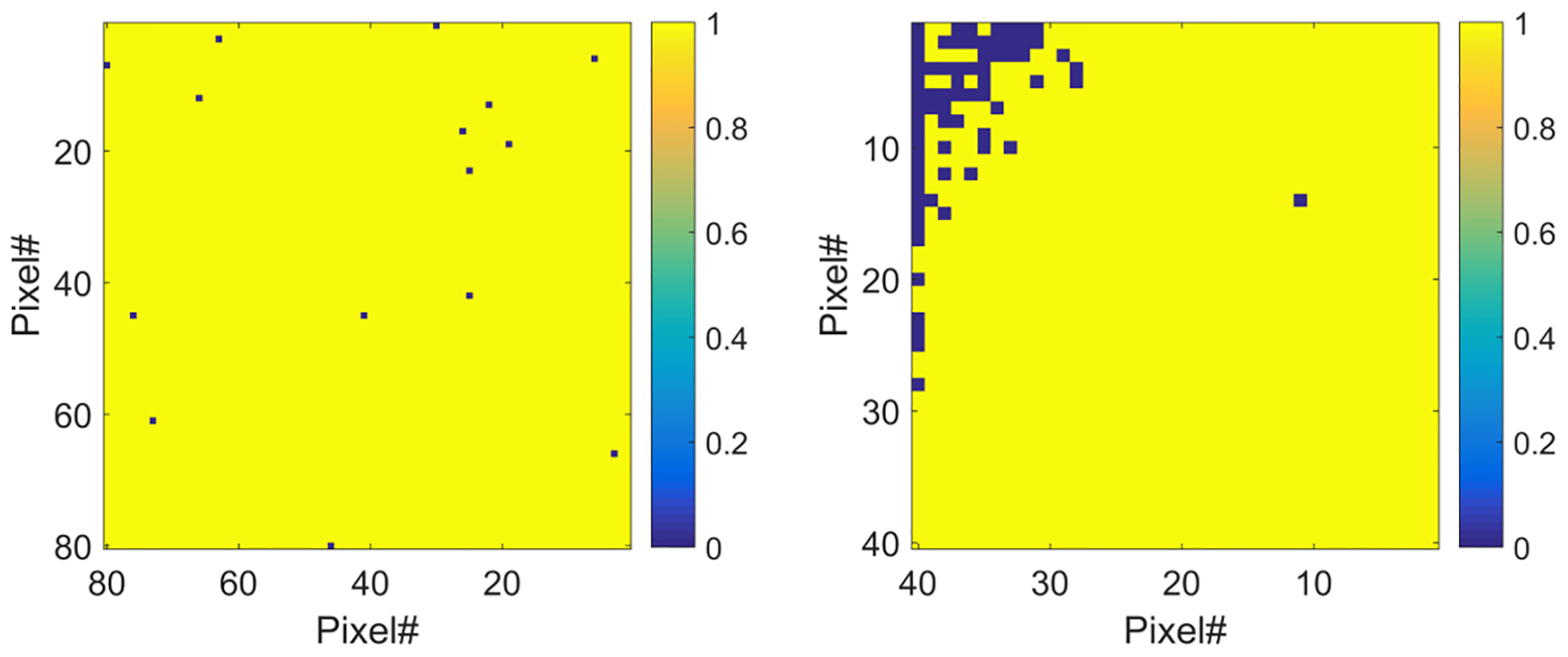
Bad Pixel maps for (left) 1-mm-thick CdTe and (right) 2-mm-thick CZT detector module. Bad pixels have value 0, good pixels 1.
Figs. 9 and 10 show the gain and offset values across all the pixels and matching histograms. The CdTe detector has an average gain of 4.28 ± 0.048 ADU/keV, while the CZT has 4.28 ± 0.18 ADU/keV. The offset shows a wider distribution around 0 with an average 0.56 ± 3.75 ADU for the CdTe detector and 1.16 ± 3.43 ADU for the CZT detector, and an overall trend of progressively higher offset values when pixels are closer to the bonding wires. To determine the spatial distribution of the total number of counts in the first and second peaks, a 6.7% asymmetric window (asymmetry ratio 0.33) is used for the first peak, while a 3.3% asymmetric window (asymmetry ratio 0.33) is used for the second peak, respectively. As expected, the number of counts in the main peaks in a 500 μm × 500 μm CZT pixel is around 4 times the number of counts in the main peaks in a 250 μm × 250 μm 1-mm CdTe pixel, accounting for the different crystal thicknesses and material efficiencies [43] at 59.5 keV and 122 keV. The pixel maps in Figs. 11–12 show a consistent uniform response in both sensors.
Fig. 9.
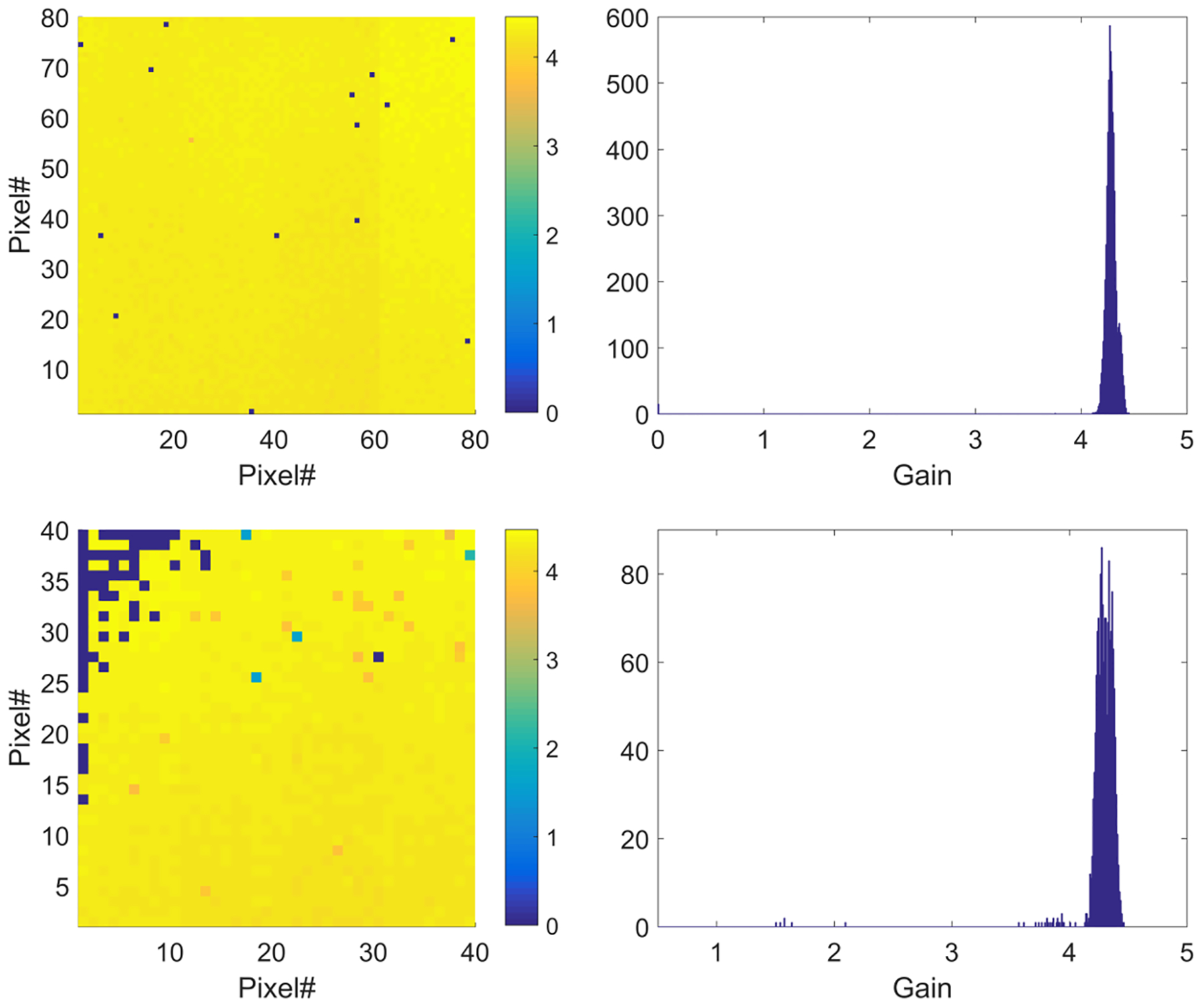
Gain pixel maps (first column) and matching histograms (second column) for 1-mm-thick CdTe (first row) and 2-mm-thick CZT (second row). The gain is given in ADU/keV. Bad pixels are not considered.
Fig. 10.
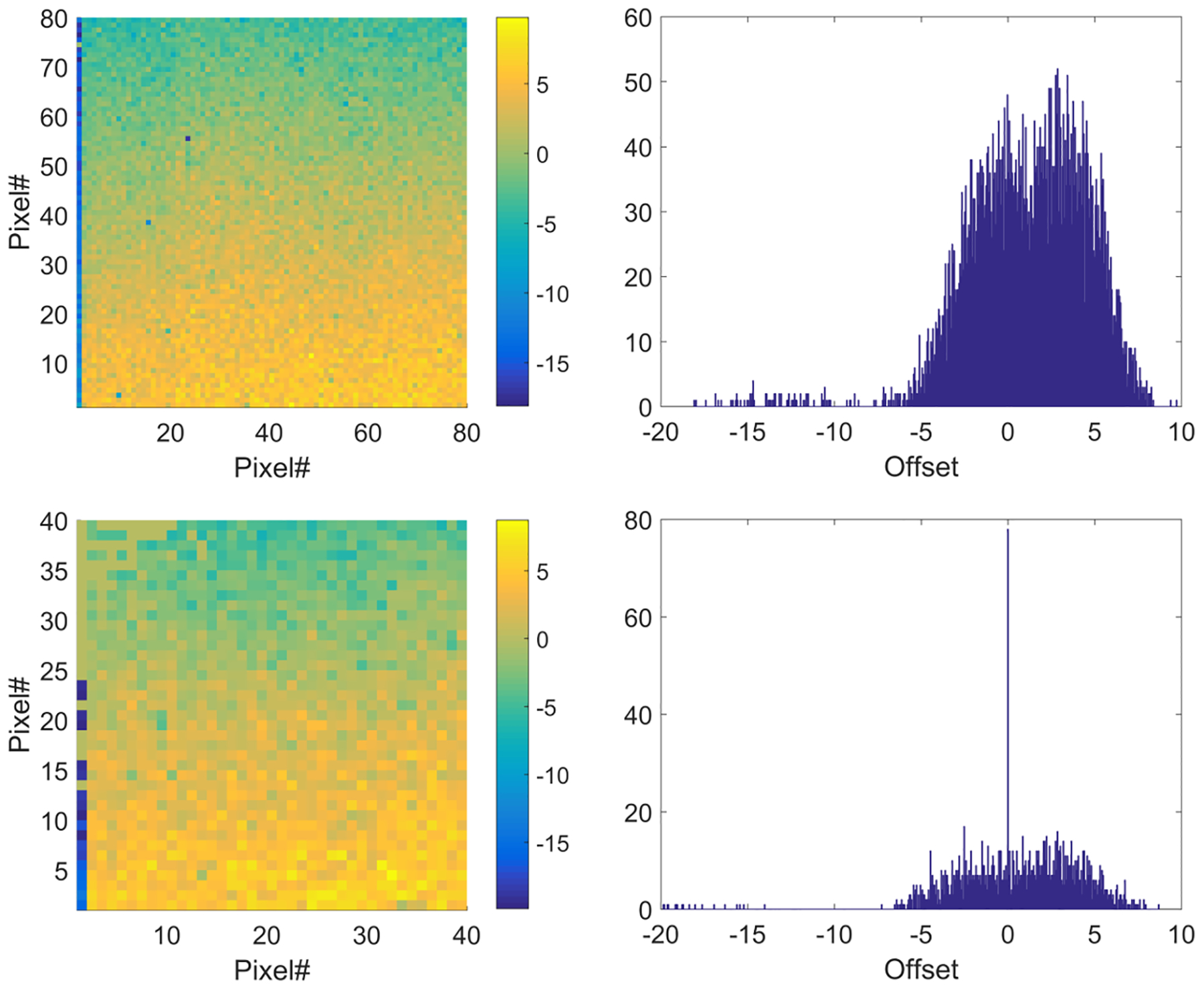
Offset pixel maps (first column) and matching histograms (second column) for 1-mm-thick CdTe (first row) and 2-mm-thick CZT (second row). The offset is given in ADU. Bad pixels are not considered.
Fig. 11.
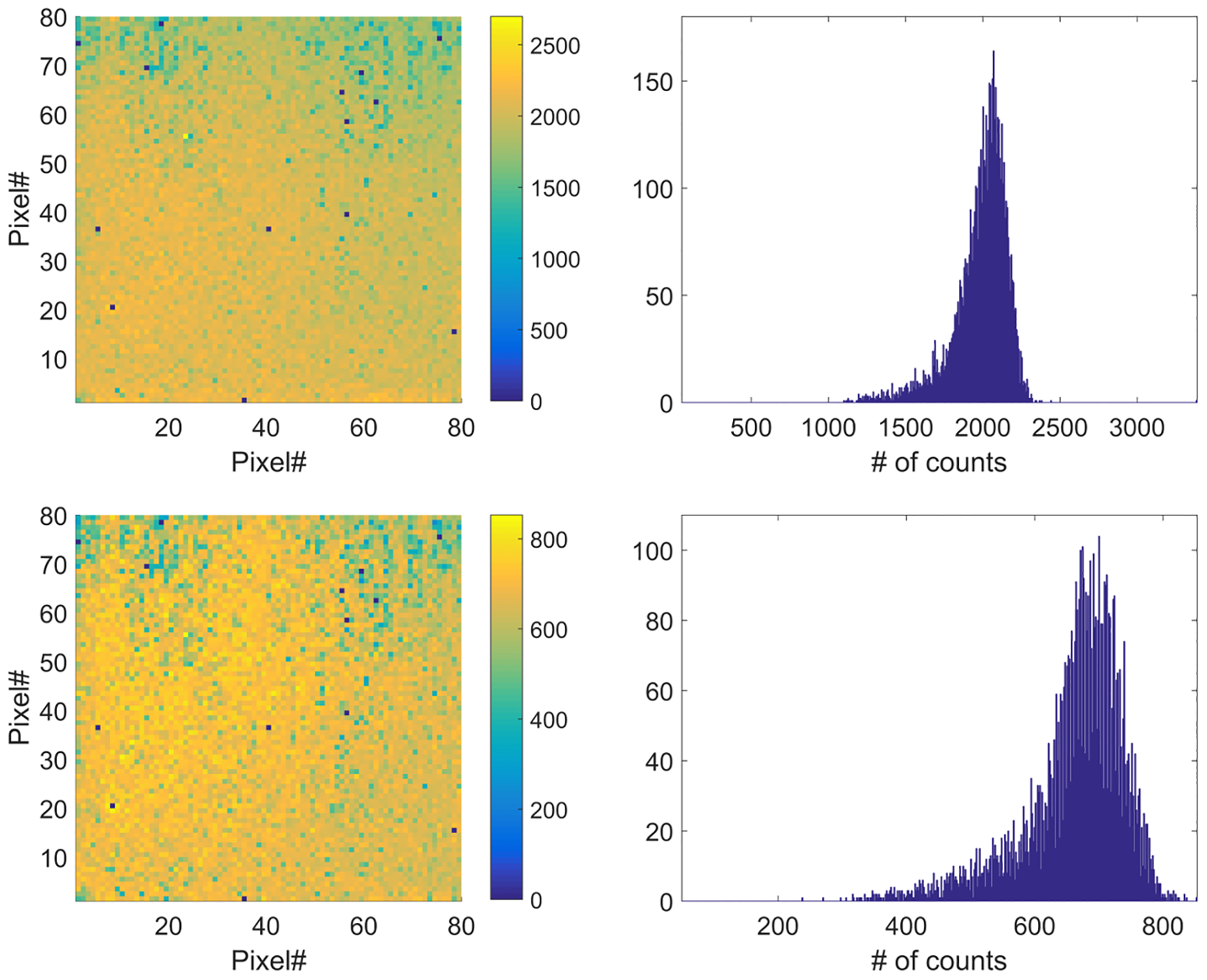
Spatial distribution and matching histograms for the total number of counts in the 59.5-keV peak (first row) and in the 122-keV peak (second row) in the 1-mm-thick CdTe detector. Bad pixels are not considered.
Fig. 12.
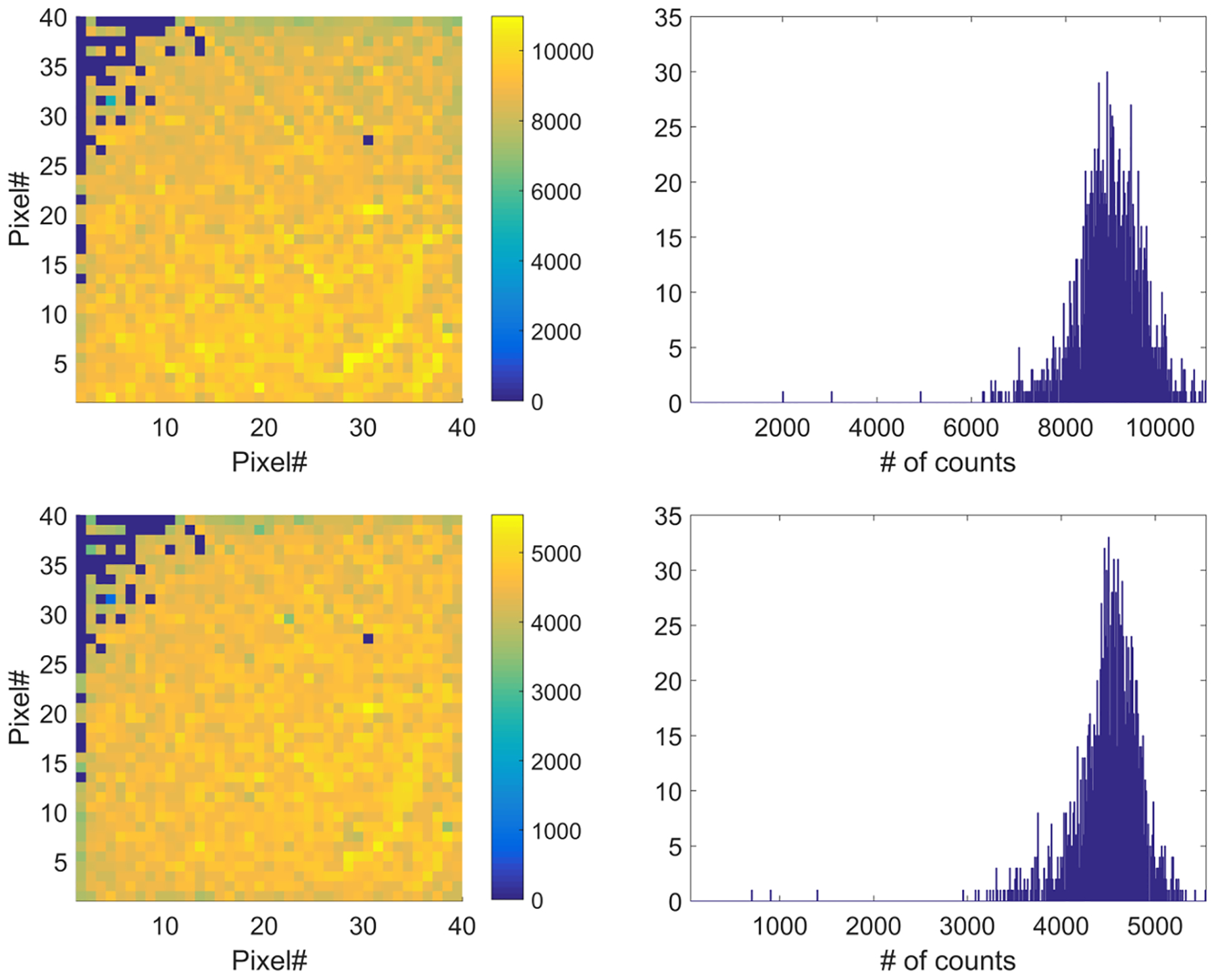
Spatial distribution and matching histograms for the total number of counts in the 59.5-keV peak (first row) and in the 122-keV peak (second row) in the 2-mm-thick CZT detector. Bad pixels are not considered.
The distribution of the FHWM values of the first and second peaks in the 1-mm-thick CdTe and 2-mm-thick CZT for all the readout channels and matching histograms are shown in Figs. 13–14, respectively. For the 1-mm-thick CdTe detector, 96.85% of pixels have the FWHM of the first peak <1.5 keV with an average FWHM of 0.80 ± 0.17 keV, and the same pixels have an average FWHM of 1.05 ± 0.30 keV for the second peak. Analogous results are found in [14,44] where a single-module HEXITEC PBC is used. The stability of the detector spectroscopic performance under different temperature operating conditions were already reported in [18], showing small changes in the detector FWHM in the 5°−30° temperature range. Similarly, for the 2-mm-thick CZT detector, 95.12% of pixels have the FWHM of the first peak <1.5 keV with an average FWHM of 0.85 ± 0.08 keV, and the same pixels have an average FWHM of 1.62 ±0.26 keV for the second peak. The results are consistent with those obtained from Redlen CZT detectors bonded on HEXITEC ASIC in [37,38]. As shown in Figs. 11–14, border pixels tend to have inferior performance because of the irregular electric field and potentially increased leakage current close to the boundary of the crystal [45].
Fig. 13.
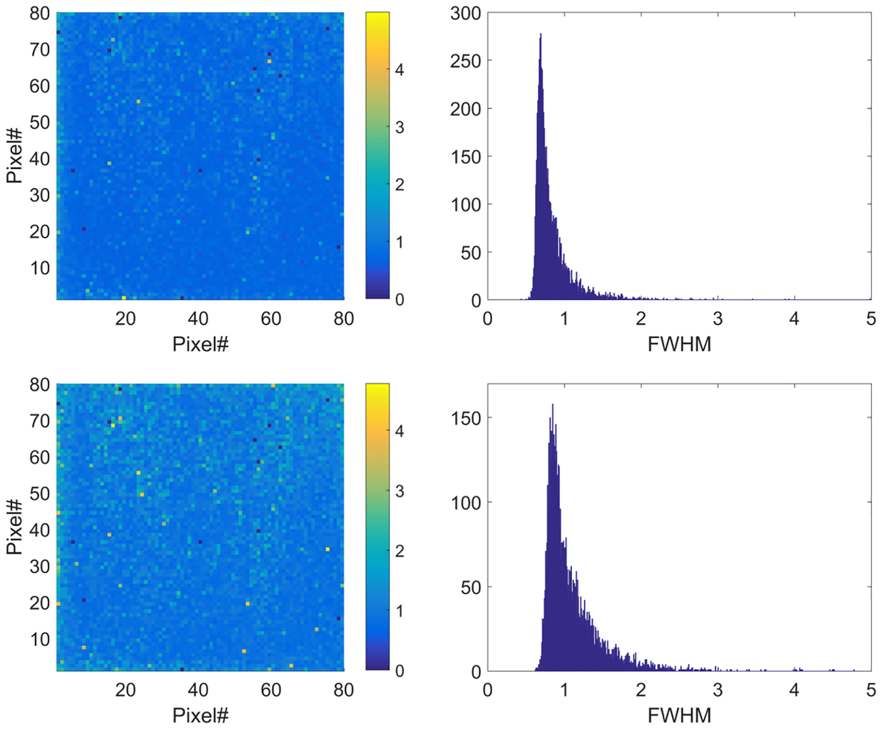
FWHM map and matching histograms for the 59.5-keV peak (first row) and 122-keV peak (second row) in the 1-mm-thick CdTe detector. The FWHM is given in keV. Bad pixels are not considered.
Fig. 14.
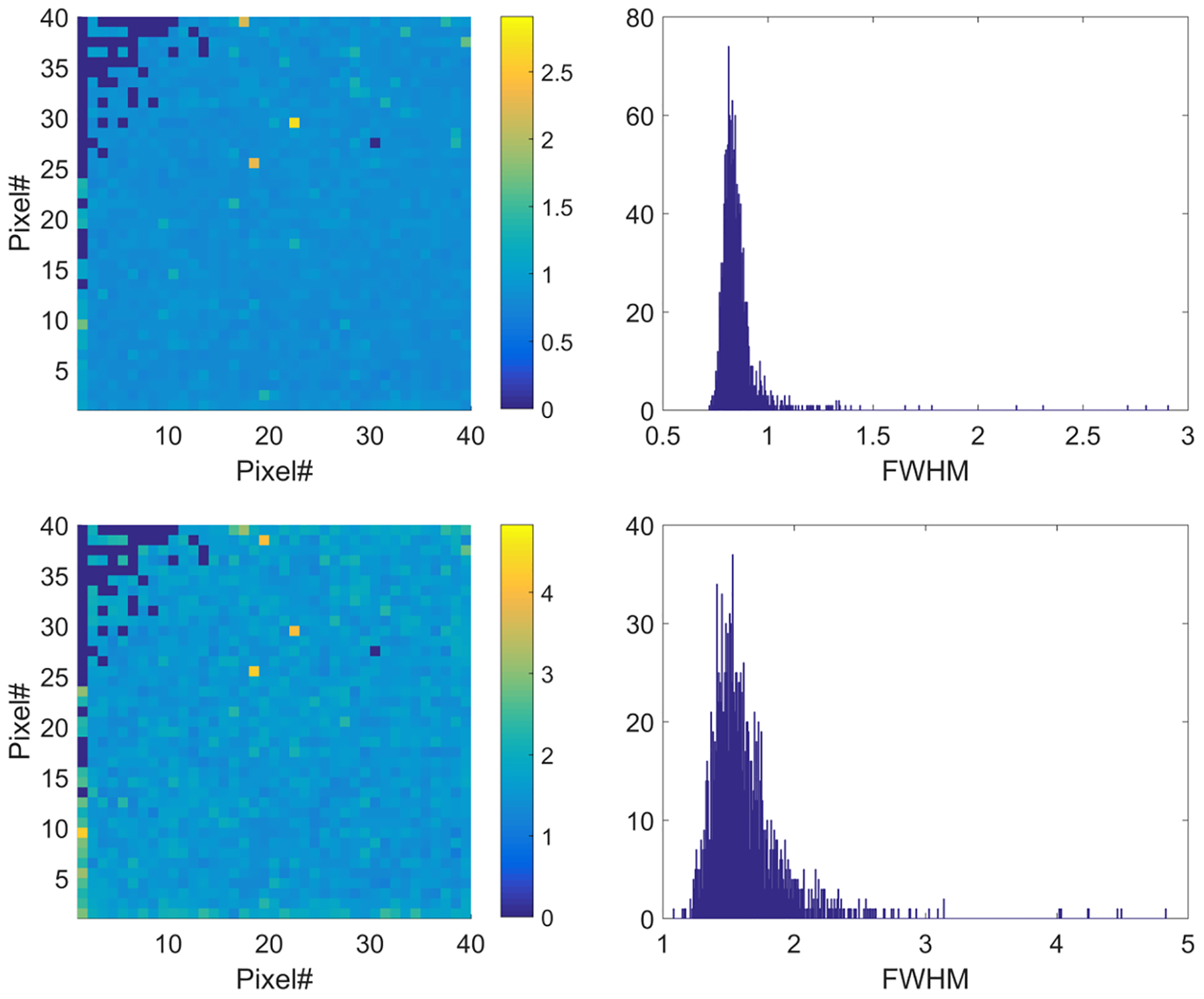
FWHM map and matching histograms for the 59.5-keV peak (first row) and 122-keV peak (second row) in the 2-mm-thick CZT detector. The FWHM is given in keV. Bad pixels are not considered.
Typical single-pixel spectra from the 1-mm-thick CdTe and 2-mm-thick CZT detectors are shown in Figs. 15–16, respectively. Fig. 17 shows the energy spectra that include all events detected by these sensors. All the spectra exhibit excellent spectroscopic performance, where the main peaks at 59.5 keV and 122 keV are sharp and clearly visible. Additionally, a cluster of Cd and Te characteristic lines and escape peaks in the 23–40 keV region and characteristic emission peaks at 17.8–18, 20.8 and 33.2 keV from Np isotopes as decay products of Am-241 are noticeable in the <50 keV region (Fig. 17, central zoomed box). All the energy spectra are corrected for gain and pedestal variations, and both the raw data and charge-sharing corrected spectra are compared in the figures.
Fig. 15.
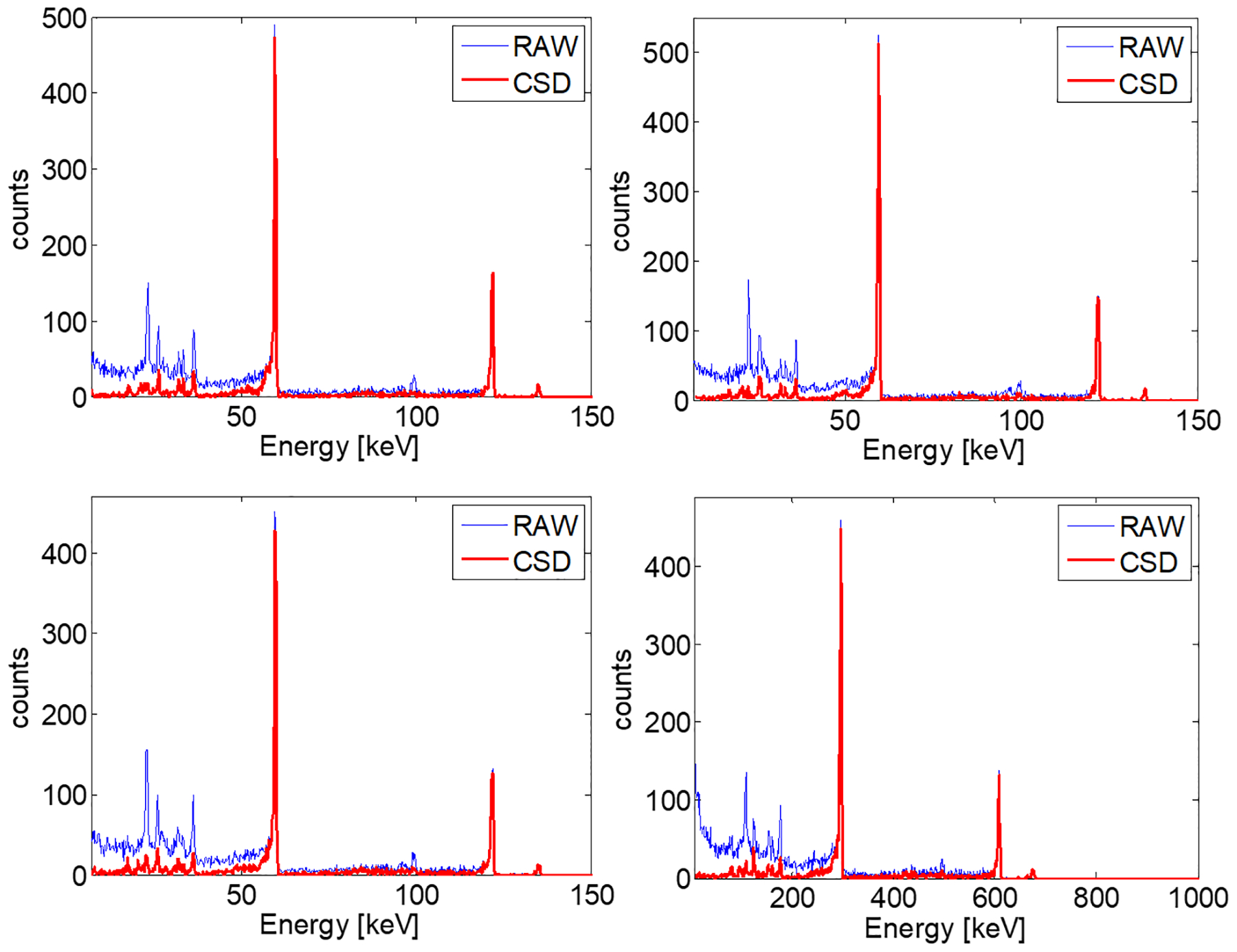
Typical single-pixel spectra from the 1-mm-thick CdTe sensor. The raw spectrum is shown in blue (thin), the charge-sharing corrected in red (thick)..
Fig. 16.
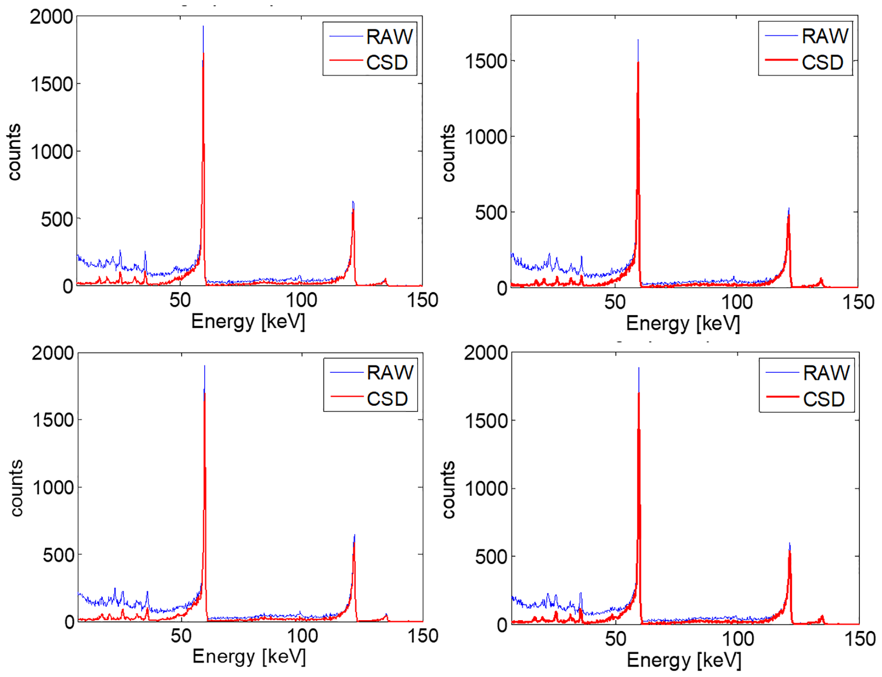
Typical single-pixel spectra from the 2-mm-thick CZT sensor. The raw spectrum is shown in blue (thin), the charge-sharing corrected in red (thick)..
Fig. 17.

Energy summed spectra from all events detected by (left) the entire 1-mm-thick CdTe sensor, (right) the entire 2-mm-thick CZT sensor. The central image is the zoomed view for <50 keV peaks, including Cd and Te characteristic lines and escape peaks and characteristic emission peaks from Np isotopes as decay products of Am-241. The raw spectrum is shown in blue (thin), the charge-sharing corrected in red (thick). Bad pixels are not included..
3.2. Detector charge sharing
To evaluate the level of charge sharing in the small-pixel detector unit, a charge sharing correction method is applied to the data using a very simple charge sharing discrimination (CSD) algorithm [18]. In every single frame, the pixel values are compared with their corresponding low-energy thresholds to determine whether there is a signal induced on each of the individual pixels. Gamma-ray interaction events inducing signals on multiple adjacent pixels in a 3 × 3 pixel region are removed from the final pixel spectrum. This procedure is less ideal since it reduces the total number of counts. However, it improves the energy resolution by reducing the low energy tailing effect. Considering the small pixel sizes in the detectors used (250 μm in CdTe and 500 μm in CZT), the charge sharing effect is considerable: for the 1-mm-thick CdTe detector with 250 μm pixel size, 60.19% of events do not have signal sharing, 30.33% events have signals shared by two edgewise adjacent pixels, 2.33% events have signals shared by a paired of diagonally-neighboring pixels, and the remaining 7.15% have signals shared by three or more pixels. For the 2-mm-thick CZT detector with 500 μm pixel size, 66.7% events show no signal-sharing, 26.1% events have signal shared by two edgewise adjacent pixel, 2.1% events have signals shared by two diagonally-neighboring pixels, and the remaining 5.1% of events have signals shared by three or more pixels. In this case, the bigger pixel size reduces the chance that a charge is shared over multiple pixels. Having ~40% of shared events in the CdTe detector and ~33% in the CZT suggests that a charge sharing correction algorithm that preserves the total number of detected events is needed, and the CSD algorithm do not represent an efficient solution. Finally, it is worth to note that the correction of charge-sharing events would improve also the spatial resolution properties of the detector unit, reducing the ambiguity of the interaction point. Based on this, other off-line correction algorithms are currently under investigation and the results will be discussed in future works.
4. Conclusions and future works
The rising demand for high energy and spatial resolution applications in medical nuclear imaging requires the complemental development of high-performance detectors and corresponding high-speed readout electronics. RTSDs, e.g. CZT or CdTe, are widely recognized as a promising replacement to bulky scintillation detectors for high-resolution nuclear imaging applications.
We have developed a compact multi-channel readout circuitry for spectroscopic imaging with small-pixel CZT and CdTe detectors read out with the HEXITEC ASIC. This is the first HEXITEC-based external readout system being designed and optimized specifically for real-world SPECT and XFCT imaging applications. These detectors offer a fine spatial resolution (250 μm or 500 μm) and excellent spectroscopic performance (0.8 keV at 60 keV and 1.05 keV at 122 keV) over a broad energy range of 20–600 keV. The readout electronics is distributed over two boards: the analog front-end PCB directly connected to two Cd(Zn)Te/HEXITEC ASIC modules provides power and controls data acquisition and transfer, and a remote DAQ board performs the back-end operations. Each DAQ board controls two analog front-end PCBs simultaneously and the two boards are connected through twisted-pair ribbon cables, up to 10 m in length. One of the main emphases in this readout development is to preserve the ultrahigh energy resolution provided by the Cd(Zn)Te/HEXITEC ASIC detector modules.
Our design is dictated by the need of a compact, flexible and scalable readout electronics that could be eventually used in full-scale clinical SPECT systems. By design, the front-end circuitry is relatively compact and is connected to a remote DAQ system with flexible cables. One could use this architecture to form large arrays of different sizes and shapes tailored for different imaging applications. The current external readout circuitry will be used to develop a partial ring for preclinical XFCT imaging applications [30,31].
Our preliminary results demonstrated that the prototype multi-channel readout circuitry delivers an excellent spectroscopic performance with Cd(Zn)Te/HEXITEC ASIC modules. Both sensors tested, a 1-mm-thick CdTe and a 2-mm-thick CZT, demonstrated an excellent uniformity of spectroscopic performance consistent with previously published results [14,38,44].
Future work is planned to address the charge sharing effect investigating other off-line correction algorithms that preserve the total number of detected events. Future development will consider the possibility to use the readout circuitry in a MR-compatible SPECT system, the MRC-SPECT-II system [28,29], that operates inside a strong magnetic field. Based on this, feasibility studies to evaluate the MR-compatibility of the circuitry will be carried out. Finally, the use of thicker crystals to improve the detection efficiency at higher energies (300–600 keV) has been considered. This would require crystals having a thickness ≥ 5 mm and a readout electronics with DOI capabilities is currently under development [39].
Acknowledgment
Research reported in this publication was supported by the National Institute of Biomedical Imaging and Bioengineering (NIBIB) under award numbers 1 R01 EB022388–01 and 1 R01 EB026300-01A1.
Footnotes
Declaration of competing interest
The authors declare that they have no known competing financial interests or personal relationships that could have appeared to influence the work reported in this paper.
References
- [1].Abbaspour S, Mahmoudian B, Islamian JP, Cadmium telluride semiconductor detector for improved spatial and energy resolution radioisotopic imaging (in eng), World J. Nucl. Med 16 (2) (2017) 101, 10.4103/1450-1147.203079. [DOI] [PMC free article] [PubMed] [Google Scholar]
- [2].Scheiber C, CdTe and CdZnTe detectors in nuclear medicine, Nucl. Instrum. Methods Phys. Res. A 448 (3) (2000) 513–524, 10.1016/S0168-9002(00)00282-5. [DOI] [Google Scholar]
- [3].Hutton BF, Erlandsson K, Thielemans K, Advances in clinical molecular imaging instrumentation, Clin. Transl. Imaging 6 (1) (2018) 31–45, 10.1007/s40336-018-0264-0. [DOI] [Google Scholar]
- [4].Jiang W, Chalich Y, Deen MJ, Sensors for positron emission tomography applications (in eng), Sensors (Basel) 19 (22) (2019) 5019, 10.3390/s19225019. [DOI] [PMC free article] [PubMed] [Google Scholar]
- [5].Park C, Song H, Joung J, Kim Y, Kim KB, Chung YH, Feasibility study of SiPM based scintillation detector for dual-energy X-ray absorptiometry, Nucl. Eng. Technol (2020) 10.1016/j.net.2020.03.030, 2020/April/03/. [DOI] [Google Scholar]
- [6].Bocher M, Blevis IM, Tsukerman L, Shrem Y, Kovalski G, Volokh L, A fast cardiac gamma camera with dynamic SPECT capabilities: design, system validation and future potential (in eng), Eur. J. Nucl. Med. Mol. Imaging 37 (10) (2010) 1887–1902, 10.1007/s00259-010-1488-z. [DOI] [PMC free article] [PubMed] [Google Scholar]
- [7].Goshen E, Beilin L, Stern E, Kenig T, Goldkorn R, Ben-Haim S, Feasibility study of a novel general purpose CZT-based digital SPECT camera: initial clinical results (in eng), EJNMMI Phys. 5 (1) (2018) 6, 10.1186/s40658-018-0205-z. [DOI] [PMC free article] [PubMed] [Google Scholar]
- [8].Hruska CB, Phillips SW, Whaley DH, Rhodes DJ, O’Connor MK, Molecular breast imaging: use of a dual-head dedicated gamma camera to detect small breast tumors (in eng), AJR Am. J. Roentgenol 191 (6) (2008) 1805–1815, 10.2214/AJR.07.3693. [DOI] [PMC free article] [PubMed] [Google Scholar]
- [9].Erlandsson K, Kacperski K, van Gramberg D, Hutton BF, Performance evaluation of D-SPECT: a novel SPECT system for nuclear cardiology, Phys. Med. Biol 54 (9) (2009) 2635–2649, 10.1088/0031-9155/54/9/003. [DOI] [PubMed] [Google Scholar]
- [10].Sharir T, Slomka PJ, Berman DS, Solid-state SPECT technology: fast and furious, J. Nucl. Cardiol 17 (5) (2010) 890–896, 10.1007/s12350-010-9284-5. [DOI] [PubMed] [Google Scholar]
- [11].Roy UN, et al. , Role of selenium addition to CdZnTe matrix for room-temperature radiation detector applications, Sci. Rep 9 (1) (2019) 1620, 10.1038/s41598-018-38188-w. [DOI] [PMC free article] [PubMed] [Google Scholar]
- [12].Iniewski K, CZT sensors for computed tomography: from crystal growth to image quality, J. Instrum 11 (12) (2016) C12034, 10.1088/1748-0221/11/12/c12034. [DOI] [Google Scholar]
- [13].Jones L, Seller P, Wilson M, Hardie A, HEXITEC ASIC-A pixellated readout chip for CZT detectors, Nucl. Instrum. Methods Phys. Res. A 604 (2009) 10.1016/j.nima.2009.01.046, June/01. [DOI] [Google Scholar]
- [14].Veale MC, Seller P, Wilson M, Liotti E, HEXITEC: A high-energy X-ray spectroscopic imaging detector for synchrotron applications, Synchrotron Radiat. News 31 (6) (2018) 28–32, 10.1080/08940886.2018.1528431. [DOI] [Google Scholar]
- [15].Scuffham JW, et al. , A cdte detector for hyperspectral SPECT imaging, J. Instrum 7 (08) (2012) P08027, 10.1088/1748-0221/7/08/p08027. [DOI] [Google Scholar]
- [16].Seller P, et al. , Pixellated Cd(Zn)Te high-energy X-ray instrument, J. Instrum 6 (12) (2011) C12009, 10.1088/1748-0221/6/12/c12009. [DOI] [PMC free article] [PubMed] [Google Scholar]
- [17].Wilson MD, et al. , A 10 cm×10 cm CdTe spectroscopic imaging detector based on the HEXITEC ASIC, J. Instrum 10 (10) (2015) P10011, 10.1088/1748-0221/10/10/p10011. [DOI] [Google Scholar]
- [18].Veale MC, et al. , Measurements of charge sharing in small pixel CdTe detectors, Nucl. Instrum. Methods Phys. Res. A 767 (2014) 218–226, 10.1016/j.nima.2014.08.036. [DOI] [Google Scholar]
- [19].Egan CK, et al. , 3D chemical imaging in the laboratory by hyperspectral X-ray computed tomography, Sci. Rep 5 (1) (2015) 15979, 10.1038/srep15979. [DOI] [PMC free article] [PubMed] [Google Scholar]
- [20].Liotti E, et al. , Mapping of multi-elements during melting and solidification using synchrotron X-rays and pixel-based spectroscopy, Sci. Rep 5 (1) (2015) 15988, 10.1038/srep15988. [DOI] [PMC free article] [PubMed] [Google Scholar]
- [21].Rakowski R, et al. , Single-shot structural analysis by high-energy X-ray diffraction using an ultrashort all-optical source, Sci. Rep 7 (1) (2017) 16603, 10.1038/s41598-017-16477-0. [DOI] [PMC free article] [PubMed] [Google Scholar]
- [22].Moss R, Crews C, Wilson M, Speller R, miniPixD: a compact sample analysis system which combines X-ray imaging and diffraction, J. Instrum 12 (02) (2017) P02001, 10.1088/1748-0221/12/02/p02001. [DOI] [Google Scholar]
- [23].Gaskin J, et al. , SuperHERO: The Next Generation Hard X-Ray HEROES Telescope, 2014, p. 91443Z.
- [24].Seller P, et al. , CdTe Focal Plane Detector for Hard X-Ray Focusing Optics, 2015.
- [25].Scuffham JW, et al. , Imaging of Ra-223 with a small-pixel CdTe detector, J. Instrum 10 (01) (2015) C01029, 10.1088/1748-0221/10/01/c01029. [DOI] [Google Scholar]
- [26].Pani S, et al. , K-edge subtraction imaging using a pixellated energy-resolving detector, in: SPIE Medical Imaging, SPIE, 2011. [Google Scholar]
- [27].Wilson MD, et al. , Multiple module pixellated CdTe spectroscopic X-ray detector, IEEE Trans. Nucl. Sci 60 (2) (2013) 1197–1200, 10.1109/TNS.2013.2240694. [DOI] [Google Scholar]
- [28].Lai X, Meng L-J, Simulation study of the second-generation MR-compatible SPECT system based on the inverted compound-eye gamma camera design, Phys. Med. Biol 63 (4) (2018) 045008, 10.1088/1361-6560/aaa4fb. [DOI] [PMC free article] [PubMed] [Google Scholar]
- [29].Zannoni EM, Lai X, Meng L-J, Design study for MRC-SPECT-II: The second generation MRI compatible SPECT system based on hyperspectral compound-eye gamma cameras, J. Nucl. Med 58 (supplement 1) (2017) 1321, [Online]. Available: http://jnm.snmjournals.org/content/58/supplement_1/1321.abstract. [Google Scholar]
- [30].Chen Y, George J, Zannoni EM, Meng L-J, A multi-contrast X-ray fluorescence, X-ray luminescence and X-ray CT functional imaging platform for in vivo imaging of non-radioactive therapeutic agents in small animals, J. Nucl. Med 59 (supplement 1) (2018) 1760, [Online]. Available: http://jnm.snmjournals.org/content/59/supplement_1/1760.abstract. [Google Scholar]
- [31].Chen Y, Nie X, Zannoni EM, L.-j. Meng, A partial ring X-ray fluorescence computed tomography imaging platform for in vivo imaging of non-radioactive metal-based therapeutic agents in small animals, J. Nucl. Med 60 (supplement 1) (2019) 318, [Google Scholar]
- [32].Bazalova M, Pratx G, Xing L, X-ray fluorescence computed tomography (XFCT) for high-sensitivity imaging of cisplatin, Int. J. Radiat. Oncol. Biol. Phys 87 (2) (2013) S646, 10.1016/j.ijrobp.2013.06.1711. [DOI] [Google Scholar]
- [33].Chen M-H, et al. , Hafnium-doped hydroxyapatite nanoparticles with ionizing radiation for lung cancer treatment, Acta Biomater. 37 (2016) 165–173, 10.1016/j.actbio.2016.04.004. [DOI] [PubMed] [Google Scholar]
- [34].Fahrni CJ, Biological applications of X-ray fluorescence microscopy: exploring the subcellular topography and speciation of transition metals, Curr. Opin. Chem. Biol 11 (2) (2007) 121, 10.1016/j.cbpa.2007.02.039. [DOI] [PubMed] [Google Scholar]
- [35].Shiraki H, Funaki M, Ando Y, Kominami S, Amemiya K, Ohno R, Improvement of the productivity in the THM growth of CdTe single crystal as nuclear radiation detector, IEEE Trans. Nucl. Sci 57 (1) (2010) 395–399, 10.1109/TNS.2009.2035316. [DOI] [Google Scholar]
- [36].Veale MC, et al. , Synchrotron characterisation of non-uniformities in a small pixel cadmium zinc telluride imaging detector, Nucl. Instrum. Methods Phys. Res. A 729 (2013) 265–272, 10.1016/j.nima.2013.07.054. [DOI] [Google Scholar]
- [37].Awadalla S, Iniewski K, CdTe and CdZnTe small pixel imaging detectors, in: Solid-State Radiation Detectors: Technology and Applications, CRC Press, 2015, pp. 56–68, ch. 3. [Google Scholar]
- [38].Wilson MD, et al. , Small pixel CZT detector for hard X-ray spectroscopy, Nucl. Instrum. Methods Phys. Res. A 652 (1) (2011) 158–161, 10.1016/j.nima.2011.01.144. [DOI] [Google Scholar]
- [39].Zhang J, Zannoni EM, Wilson M, Meng L-J, Development of 3D HEXITEC CdZnTe detector - A large area high-resolution γ-ray imaging camera for future SPECT imaging, J. Nucl. Med 59 (supplement 1) (2018) 1770a, [Online]. Available: http://jnm.snmjournals.org/content/59/supplement_1/1770a.abstract. [Google Scholar]
- [40].Bell RO, Entine G, Serreze HB, Time-dependent polarization of CdTe gamma-ray detectors, Nucl. Instrum. Methods 117 (1) (1974) 267–271, 10.1016/0029-554X(74)90408-X. [DOI] [Google Scholar]
- [41].Hazlett T, et al. , Large, high resolution CdTe gamma ray sensors, IEEE Trans. Nucl. Sci 33 (1) (1986) 332–335, 10.1109/TNS.1986.4337112. [DOI] [Google Scholar]
- [42].Seino T, Takahashi I, CdTe detector characteristics at 30° and 35° when using the periodic bias reset technique, IEEE Trans. Nucl. Sci 54 (4) (2007) 777–781, 10.1109/TNS.2007.897034. [DOI] [Google Scholar]
- [43].Redus B, Efficiency of Amptek XR-100T-CdTe and -CZT Detectors Application Note ANCZT-1 Rev 2, Amptek Inc., 2002. [Google Scholar]
- [44].Veale MC, Bell SJ, Seller P, Wilson MD, Kachkanov V, X-ray micro-beam characterization of a small pixel spectroscopic CdTe detector, J. Instrum 7 (07) (2012) P07017, 10.1088/1748-0221/7/07/p07017. [DOI] [Google Scholar]
- [45].Duarte DD, et al. , Edge effects in a small pixel CdTe for X-ray imaging, J. Instrum 8 (10) (2013) P10018, 10.1088/1748-0221/8/10/p10018. [DOI] [Google Scholar]


