Figure 1.
Fabrication of Flexible In2O3 Nanoribbon Biosensors
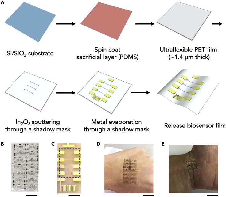
(A) Schematic of the fabrication process. Each Si/SiO2 substrate was coated with a polydimethylsiloxane (PDMS) adhesion layer. Next, a 1.4-μm polyethylene terephthalate (PET) film was laminated over the PDMS. The In2O3 nanoribbons were patterned by sputtering on the PET layer through a shadow mask. A 1-nm Ti adhesion layer followed by a 50-nm Au layer were deposited through a different shadow mask to pattern source, drain, gate, and temperature sensor electrodes. The biosensor film was then delaminated from the rigid carrier wafer.
(B) Photograph of as-fabricated device array. Scale bar is 1 cm. Each array has 14 devices with four field-effect transistors (FETs) per device.
(C) Optical microscope image of a single device showing the Au common-gate electrode, four In2O3 nanoribbon FETs (dotted blue box), and a Au resistive temperature sensor (from top to bottom). The low contrast of the In2O3 nanoribbons is due to their transparency. Scale bar is 500 μm.
(D) Flexibility of a sensor array is illustrated by conformal attachment to human skin. Scale bar is 2 cm.
(E) Biosensor film wrinkled during human body movement. Scale bar is 1 cm.
See also Figure S1.

