Abstract
Compared to colloidal quantum dots, nanostructured multilayer films may also be a promising emission layer in future light-emitting diodes, due to their excellent photoluminescence (PL), narrow full width at half-maximum (FWHM), and wide color gamut. In this paper, multilayer-structured deep-blue light-emitting diodes (LEDs) were prepared, where nanostructured ZnSe/ZnS multilayer films act as the light-emitting layer. The device showed good blue electroluminescence (EL) spectrum locating at 448 nm with an FWHM of 31 nm. To improve the performance of the device, the effect of preparation parameters of different layers was investigated in detail. The results demonstrated that the preparation parameters of each layer affected the performance in different ways, and choosing the most suitable preparation parameters can achieve optimal performance. Furthermore, this multilayer-structured device based on nanostructured films as emission layer can also be applied in green and red LEDs or all-inorganic QLEDs.
1. Introduction
With the rapid development of information technology, the display field faces enormous opportunities and challenges. In the past decades, light-emitting diodes based on colloidal quantum dots1−3 have been attracting increasing attention. Quantum dots (QDs) have excellent properties, including high color purity, high photoluminescence (PL) quantum yield,4 and good stability.5 In particular, tunable emission wavelength based on the size of particles can cover the entire visible light area. These studies mainly focused on Cd-based QDs, such as CdSe QDs,6 CdS QDs,7 CdS/ZnS QDs,8 CdSe/CdS core/shell QDs,9 and CdSe/ZnS/CdS/ZnS core/multishell QDs.10 However, due to the toxicity of Cd, the application of Cd-QDs and related devices is greatly limited, especially in the biological field.11,12 On the other hand, the heterojunction structure can make full use of the different properties of the two materials constituting the heterojunction and has excellent properties, including strong quantum effect, large mobility, and peculiar two-dimensional space characteristics. It has been widely used in many different fields such as double-heterojunction ZnS/ZnSe/CdTe used in photovoltaic structure,13 transparent p-NiO/n-ZnO heterojunction applied in devices for ultraviolet photodetectors,14 and especially in heterojunction solar cells.15,16
Therefore, it is very meaningful to combine the advantages of nanomaterials and heterojunctions. We propose to prepare a kind of blue electroluminescent devices based on ZnSe/ZnS nanoheterogeneous films as the light-emitting layer (EML) and expect to take the best advantages of the properties of ZnSe and nanostructured heterojunction. First of all, compared to CdS and CdSe, ZnSe has significant advantages in the UV-blue region due to the larger band gap of 2.7 eV17 and less toxicity.18 It is resulted that ZnSe has been used in many photoelectric fields, including lasers,19 thin-film transistors,20 cell imaging,21 blue light-emitting devices,22 solar cells,23 etc. Second, nanostructured films and quantum dots have similar properties, such as high luminous efficiency, good stability, and adjustable emission spectra. Finally, in our previous research, nanostructured ZnSe/ZnS multilayer thin films with excellent blue photoluminescence (PL) have been prepared by electron beam evaporation, where ZnSe acts as a light-emitting layer and ZnS acts as a passivation layer,24 which makes full use of the unique properties of ZnSe and ZnS in the heterojunction.
In this study, we reported on the demonstration of multilayer-structured deep-blue LEDs, where nanostructured ZnSe/ZnS multilayer films act as EML. Then, to improve the performance of device, we mainly studied the effects of different structural layers on device performance, including annealing temperature, thickness of P-type layer as well as substrate. Blue LEDs are one of the key parts in full-color electroluminescent displays and white LEDs. We hope that this novel structure will contribute to the research of blue LEDs and offer a new direction for the realization of full-color displays (Figure 1).
Figure 1.
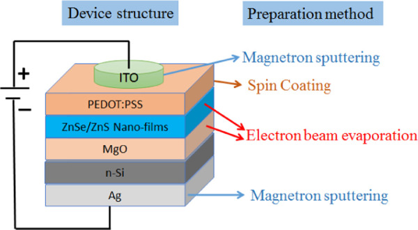
Schematic structure of blue LEDs based on nanostructured ZnSe/ZnS multilayer films.
2. Results and Discussion
2.1. Crystalline Structures
To determine the crystallinity of the ZnS/ZnSe multilayer film, we performed X-ray diffraction (XRD) of ZnSe particles, ZnS particles, and annealed nanostructured ZnSe/ZnS multilayer thin films, as shown in Figure 2. Some strong and weak diffraction peaks are observed. The planes (002), (110), and (112) of ZnS particle locate at 2θ ≈ 28.5, 47.5, and 56.4°, respectively, corresponding to wurtzite ZnS structure (JCPDS: 79-2204). The diffraction peaks of ZnSe particle at 2θ ≈ 27.2, 45.2, and 53.5° are attributed to the (111), (220), and (311) planes, respectively, in agreement with the cubic ZnSe structure (JCPDS:88-2345). However, the strength of the crystallization peak changes after the multilayer film is prepared. The peaks (200) and (220) of ZnSe locate at 2θ ≈ 31.5 and 45.2°, respectively, which also agree well with the cubic ZnSe structure (JCPDS: 88-2345). The diffraction peaks at 2θ ≈ 28.5, 47.5, and 56.4° correspond to the (002), (110), and (112) crystal orientations of wurtzite ZnS structure (JCPDS: 79-2204). In addition, the other diffraction peak at 2θ ≈ 33.1° comes from Si substrate. It is confirmed that the annealed films tend to grow in certain specific crystal directions and have good crystal quality, being beneficial to device performance.
Figure 2.
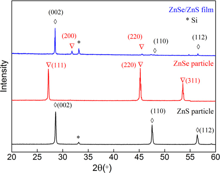
XRD patterns of ZnSe particle, ZnS particle, and annealed nanostructured ZnSe/ZnS multilayer thin film.
2.2. Device Characterization
The electroluminescence (EL) test of the device is shown in Figure 3a. It can be seen that the I–V curve has typical diode characteristic under forward bias. The turn-on voltage is about 16.5 V, which is slightly higher than those of other hybrid quantum dot devices.25,26 It is reported that the insulating property of MgO and the weak conductivity of the thick ZnS layer lead to this phenomenon.27 The current increased significantly with increasing forward bias. When the turn-on voltage is 24 V, the current of the device can reach up to approximately 12 mA. The inset is an electroluminescent photo at a voltage of 24 V in a dark environment, showing bright blue color. The corresponding electroluminescence spectrum locates at 448 nm with a full width at half-maximum (FWHM) of 31 nm. By calculating the electroluminescence spectrum, the color coordinates of (0.19, 0.08) can be obtained, which is close to the saturated deep blue color shown in Figure 3b.
Figure 3.
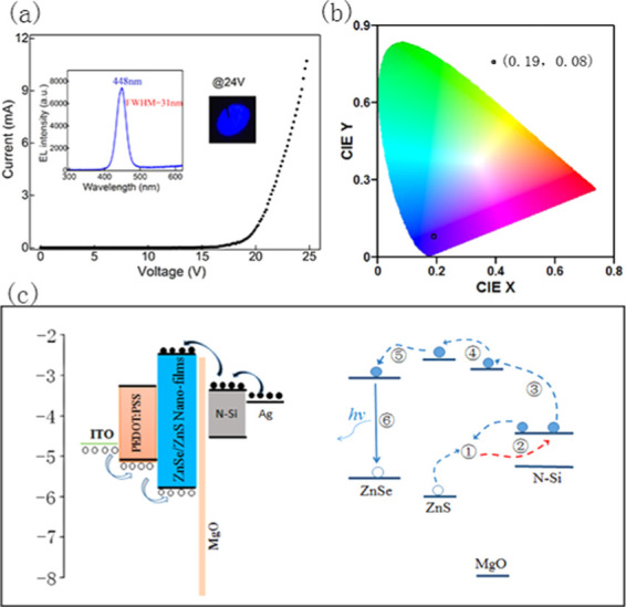
Characterization of device performance: (a) I–V curve of the device; the inset shows the EL spectrum and EL photograph at 23 V. (b) CIE of the device. (c) Detailed electroluminescence mechanism of the device.
The electroluminescence mechanism of the device where nanostructured ZnSe/ZnS multilayer thin films act as light-emitting layer (EML) is analyzed. The detailed energy-level structure and electroluminescence mechanism of the blue LEDs are shown in Figure 3c. Figure 3c (left) shows that the electroluminescence mechanism of the device is electron–hole composite luminescence. Due to the smaller band offset between PEDOT:PSS and EML than that between Si and EML, it is easier for holes to inject into EML than electronics. In addition, due to the blocking effect of the MgO layer, the holes will accumulate at the EML/MgO layer interface. Therefore, compared to PEDOT/EML, the recombination position of electrons and holes in the EML is closer to the side of MgO layer and still occurs in the light-emitting layer. The specific composite process of electron–hole is shown in Figure 3c (right). First, electrons tunneling through MgO thin films recombine with the accumulated holes, forming interfacial charges transfer (CT) excitons, or exciplex states. Second, energy will be released by the recombination of these CT excitons and then transferred to the proximal electrons coming from n-Si through an Auger process. Third, many high-energy electrons are produced after absorbing energy, which can tunnel through the thin MgO layer and inject into the conduction band of MgO or ZnS more easily. Because the conduction band energy of ZnS is higher than that of ZnSe, these high-energy electrons can inject into the conduction band of ZnSe successfully. Finally, the recombination of high-energy electrons and holes derived from the valence band of ZnSe will release photons, whose emission energy is equal to the band gap of ZnSe.
2.3. Influence of Annealing Temperature
To improve the performance of the device, we first studied the effect of annealing temperature. A series of devices (SI) with different annealing temperatures (620, 640, 660, 680 °C) were prepared, named as S1, S2, S3, and S4, respectively. The detailed preparation parameters are shown in Table 1.
Table 1. Different Preparation Parameters of the Devices (SI, SII, and SIII).
| preparation parameter | thickness of MgO layer (nm) | annealing temperature (°C) | spin coating speed of PEDOT:PSS (rpm) | resistivity of substrate (Ω·cm) |
|---|---|---|---|---|
| SI | 10 | 620, 640, 660, 680 | 4000 | 0.005 |
| SII | 660 | 3000, 3500, 4000, 4500, 5000 | 0.005 | |
| SIII | 660 | 0.005, 2–4 |
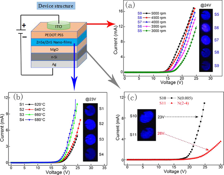
It is reported that annealing temperature mainly affects the crystal quality of the films, which is beneficial to improve the performance of the device. All of the devices with different annealing temperatures have typical diode characteristic under forward bias, as demonstrated in Figure 4. As the annealing temperature increases, the current gradually increases. The insets show the EL photographs of the different devices at 23 V in a dark environment. It can be observed that the brightness shows different trends. The EL photograph of the device annealed at 660 °C shows brighter intensity and better uniformity than other temperatures.
Figure 4.
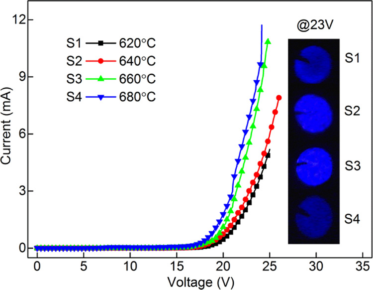
I–V curves of the devices with different annealing temperatures. The insets show the corresponding EL photographs of the devices at 23 V.
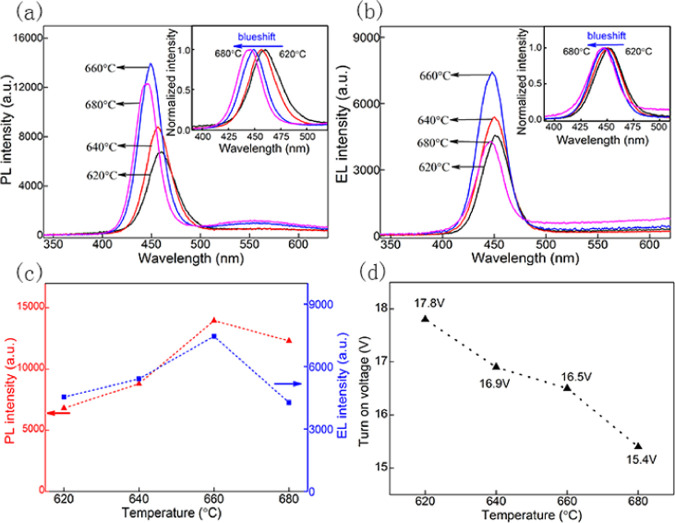
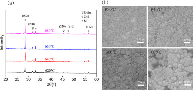
The effects of temperature on the device are further analyzed through EL, PL, and turn-on voltage, as shown in Figure 5. From Figure 5a,b, it can be seen that the PL and EL intensity first increases and then decreases, as the annealing temperature increases. The position of the luminescence peak is blue-shifted simultaneously. The intensity trends of PL and EL are the same, as shown in Figure 5c. Both the PL and EL intensities reach a maximum at 660 °C. Therefore, we can conclude that electroluminescence of devices depends on the photoluminescence of EML. As our previous reports, annealing temperature affects the properties of nanostructured ZnSe/ZnS multilayer thin films directly.24Figure 6 describes the XRD and scanning electron microscopy (SEM) images of nanostructured ZnSe/ZnS multilayer thin films annealed at different temperatures ranging from 620 to 680 °C. It can be observed that as the annealing temperature increases, the intensity of the crystallization peak first increases and then decreases, reaching the highest value at 660 °C, as shown in Figure 6a. Generally speaking, a higher annealing temperature leads to better crystallization, resulting in enhanced luminescence efficiency. Nevertheless, the degree of crystallization can be damaged by an excessively high temperature, reducing the crystallinity and PL intensity. In addition, the size of the nanofilms crystalline particles gradually increases from 620 to 680 °C, as shown in Figure 6b. The change in the crystalline size at higher temperature could be another reason for the observed blue shift of the PL. Furthermore, S and Se will lose more at higher annealing temperatures. Thinner films make total resistance of the device lower, which results in increasing current and decreasing turn-on voltage, as demonstrated in Figure 5d.
Figure 5.
Variation of different parameters of the device with temperature: (a) PL spectra; (b) EL spectra; (c) comparison of EL and PL trends; and (d) turn-on voltage of the devices.
Figure 6.
XRD patterns (a) and SEM images (b) of nanostructured ZnSe/ZnS multilayer thin film annealed at different temperatures ranging from 620 to 680 °C.
2.4. Influence of P-Type Layer Thickness
Spin-coated PEDOT:PSS was used as a hole injection layer in our device. The effect of different thicknesses of PEDOT:PSS on device performance was also investigated. A series of devices (SII) with different thicknesses of PEDOT:PSS were prepared using different rotation rates to control the thickness of PEDOT:PSS during spin coating. The detailed parameters are shown in Table 1, i.e., S5, S6, S7, S8, and S9.
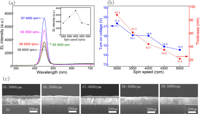
Figure 7 describes the I–V curves of the devices with different thicknesses of PEDOT:PSS. All of the devices show representative diode characteristics. It can be observed that the current of devices increases obviously with an increase rotation rate from 3000 to 5000 rpm. However, the EL intensity has not been increasing all of the time, as shown in the EL photographs of the devices at 24 V. The corresponding EL intensity is demonstrated in Figure 8a. As the rotation rate increases, the EL intensity first increases and then decreases, reaching a maximum at 4000 rpm spin speed. It is believed that the spin speed has a direct effect on the thickness of the films. The thickness of the PEDOT:PSS gradually becomes thinner as the spin speed increases. The cross-sectional SEM images of the devices were characterized, as shown in Figure 8c. It is observed that the thickness of PEDOT:PSS decreases with the increasing rotation rate. It changes from 87.4 to 21.6 nm when the rotation rate increases from 3000 to 5000 rpm, as shown in Figure 8b. The thinner P-type layer further reduces the overall resistance of the device. Therefore, the turn-on voltage of the device lowers and the current increases. Furthermore, electron–hole balance is one of the key factors affecting device performance.28 If the thickness of the PEDOT:PSS layer is too thin, the hole injection concentration will decrease, reducing the effective recombination amount of the electron–hole. Further, poor electron–hole balance will weaken the EL intensity. Therefore, the optimum spin speed is 4000 rpm in this device, corresponding to about 43.7 nm of the PEDOT:PSS film.
Figure 7.
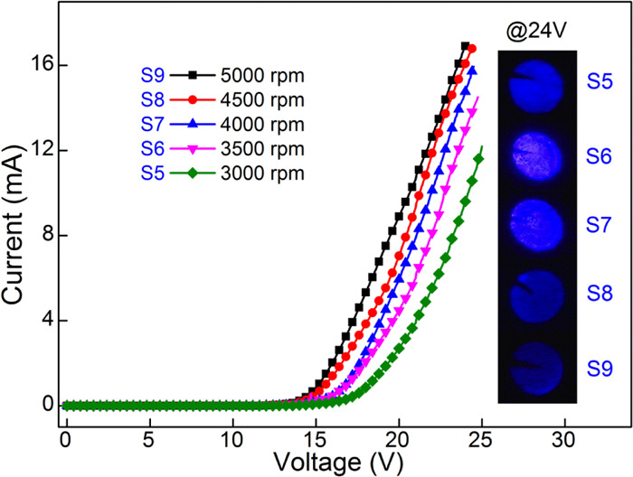
I–V curves of the devices with different rotation rates of PEDOT:PSS. The insets show the EL photographs of the devices at 24 V.
Figure 8.
Variation of parameters of the device with spin speed of PEDOT:PSS: (a) EL spectra; (b) thickness of PEDOT:PSS and turn-on voltage of the device; and (c) cross-sectional SEM images of the devices.
2.5. Influence of Substrate
Furthermore, the effect of n-Si substrate with different resistivities on device performance is also investigated. Two kinds of n-Si substrates with different resistivities of 0.005 and 2–4 Ω·cm were used in the devices, named as S10 and S11, respectively. The relevant I–V test results are shown in Figure 9. The inset shows the EL photographs at different voltages. It is clear that the device with lower-resistivity substrate has better performance, greater current, and stronger electroluminescence. The substrate with a lower resistivity has a higher doping concentration, with the ability of injecting more electrons. It also reduces the total resistance of the device. Therefore, selecting a substrate with a lower resistivity is more beneficial to improve the performance of the device.
Figure 9.
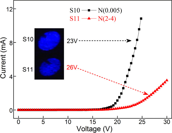
I–V curves of the devices with different resistivities of n-Si substrate.
In fact, the effect of the thickness of the MgO layer on the device had also been explored, as reported in our previous article.27 Herein, we will not discuss it in detail in this paper. In brief, the MgO films as interfacial modification layer not only improve the crystallization quality and increase the compactness of the nanostructured ZnSe/ZnS multilayer thin films but also greatly suppress exciton quenching and enhance the EL intensity. The optimum thickness of MgO films is about 10 nm. Therefore, appropriate structure layer and other oxide and preparation parameters to reduce the turn-on voltage and improve the performance of the device are very meaningful.
3. Conclusions
In summary, we successfully demonstrated high-performance multilayer-structured deep-blue LEDs, where nanostructured ZnSe/ZnS multilayer films act as the light-emitting layer, MgO film acts as the interfacial modification layer, and PEDOT:PSS acts as the hole injection layer. This device exhibits saturated deep blue color, locating at 448 nm with a FWHM of 31 nm. In addition, the effects of different structural layers on device performance were investigated. The annealing temperature mainly affected the properties of nanostructured ZnSe/ZnS multilayer films, including crystal quality, PL strength, and film thickness. The thickness of PEDOT:PSS had influence on hole injection concentration. The resistivity of substrate affected electron injection and resistance of the device distinctly. Therefore, choosing suitable preparation parameters can achieve optimal performance. Furthermore, this multilayer-structured device using nanostructured films as a light-emitting layer can also be applied in green and red LEDs or all-inorganic QLEDs.
4. Experimental Section
In this work, three series of novel blue LEDs with high-quality nanostructured ZnSe/ZnS multilayer thin films as EML were fabricated, which have different annealing temperatures, thicknesses of P-type layer, as well as different substrates. The basic structure of the device consisted of ITO/PEDOT:PSS/EML/MgO/n-Si/Ag, and each structural layer was prepared by the preparation method shown in Figure 1. The purchased ZnSe particles (99.99%, purity), ZnS particles (99.99%, purity), MgO particles (99.99%, purity), and PEDOT:PSS solution (1.4%, concentration) were used directly, without any further purification or treatment. The detailed preparation processes and parameters were as follows. First, 10 nm MgO films were deposited on n-Si substrate by electron beam evaporation, with growth rates of 0.5–0.6 Å/s. Second, 3.5 nm ZnSe and 14 nm ZnS films were alternately deposited on MgO films. The total layers of ZnSe and ZnS were 20. The growth rates were 0.5–0.6 and 0.8–1.0 Å/s, respectively. During this deposition process, the vacuum of the cavity was maintained 2.0 × 10⁻³ Pa. Third, the deposited multilayer films were annealed in a quartz tube for an hour, with a 200 sccm flow rate of N2. Fourth, 200 μL of the PEDOT:PSS solution was dropped on the annealed films and spin-coated with different rotating speeds for 20 s in air. Before spin coating, the annealed films were treated in an ultraviolet environment for 15 min. After spin coating, the films were annealed again at 150 °C for 10 min in air. Finally, 100 nm ITO as cathode and 150 nm Ag as anode electrodes were deposited on the surface of the films and the back side of Si substrate by magnetron sputtering, respectively. All of the performances of devices were measured directly at room temperature in air, without any packaging.
The XRD measurements of ZnSe particles, ZnS particles, and nanostructured ZnSe/ZnS multilayer films were made on a Bruker D8 X-ray diffractometer, using a Cu-Kr radiation source (λ = 1.5405 Å). The XRD patterns ranged from 20 to 60°, with a step size of 0.02° and a scan rate of 2°/min. The morphologies of the surface and cross-section were characterized by scanning electron microscopy (SEM). The current–voltage (I–V) characteristics of the devices were tested by a Keithley 2410 device. The photoluminescence (PL) and electroluminescence (EL) spectra were obtained by an ACTON 150 CCD spectrometer.
Acknowledgments
This work was financially supported by Fundamental Research Funds for the Central Universities (A0920502052001-242) and by the National Natural Science Foundation of China (grant no. 61975008). It was also supported by Natural Science Foundation of Ningbo (no. 2019A610068).
Author Contributions
All authors contributed equally to this work. The authors declare no competing financial interest.
The authors declare no competing financial interest.
References
- Caruge J. M.; Halpert J. E.; Wood V.; Bulović V.; Bawendi M. G. Colloidal quantum-dot light-emitting diodes with metal-oxide charge transport layers. Nat. Photonics 2008, 2, 247–250. 10.1038/nphoton.2008.34. [DOI] [Google Scholar]
- Wood V.; Bulovic V. Colloidal quantum dot light-emitting devices. Nano Rev. 2010, 1, 5202. 10.3402/nano.v1i0.5202. [DOI] [PMC free article] [PubMed] [Google Scholar]
- Kwak J.; Bae W. K.; Lee D.; Park I.; Lim J.; Park M.; Cho H.; Woo H.; Yoon D. Y.; Char K.; Lee S.; Lee C. Bright and efficient full-color colloidal quantum dot light-emitting diodes using an inverted device structure. Nano Lett. 2012, 12, 2362–2366. 10.1021/nl3003254. [DOI] [PubMed] [Google Scholar]
- Cao F.; Wang H.; Shen P.; Li X.; Zheng Y.; Shang Y.; Zhang J.; Ning Z.; Yang X. High-Efficiency and Stable Quantum Dot Light-Emitting Diodes Enabled by a Solution-Processed Metal-Doped Nickel Oxide Hole Injection Interfacial Layer. Adv. Funct. Mater. 2017, 27, 1704278 10.1002/adfm.201704278. [DOI] [Google Scholar]
- Jin X.; Li H.; Huang S.; Gu X.; Shen H.; Li D.; Zhang X.; Zhang Q.; Li F.; Li Q. Bright alloy type-II quantum dots and their application to light-emitting diodes. J. Colloid Interface Sci. 2018, 510, 376–383. 10.1016/j.jcis.2017.09.080. [DOI] [PubMed] [Google Scholar]
- Selvan S. T.; Tan T. T.; Ying J. Y. Robust, non-cytotoxic, silica-coated CdSe quantum dots with efficient photoluminescence. Adv. Mater. 2005, 17, 1620–1625. 10.1002/adma.200401960. [DOI] [Google Scholar]
- Karan S.; Majumder M.; Mallik B. Controlled surface trap state photoluminescence from CdS QDs impregnated in poly(methyl methacrylate). Photochem. Photobiol. Sci. 2012, 11, 1220–1232. 10.1039/c2pp25023c. [DOI] [PubMed] [Google Scholar]
- Hofman E.; Robinson R. J.; Li Z. J.; Dzikovski B.; Zheng W. Controlled Dopant Migration in CdS/ZnS Core/Shell Quantum Dots. J. Am. Chem. Soc. 2017, 139, 8878–8885. 10.1021/jacs.7b02320. [DOI] [PubMed] [Google Scholar]
- Li Z.-J.; Fan X.-B.; Li X.-B.; Li J.-X.; Zhan F.; Tao Y.; Zhang X.; Kong Q.-Y.; Zhao N.-J.; Zhang J.-P.; Ye C.; Gao Y.-J.; Wang X.-Z.; Meng Q.-Y.; Feng K.; Chen B.; Tung C.-H.; Wu L.-Z. Direct synthesis of all-inorganic heterostructured CdSe/CdS QDs in aqueous solution for improved photocatalytic hydrogen generation. J. Mater. Chem. A. 2017, 5, 10365–10373. 10.1039/c7ta01670k. [DOI] [Google Scholar]
- Dayneko S.; Lypenko D.; Linkov P.; Sannikova N.; Samokhvalov P.; Nikitenko V.; Chistyakov A. Application of CdSe/ZnS/CdS/ZnS Core–multishell Quantum Dots to Modern OLED Technology. Mater. Today: Proc. 2016, 3, 211–215. 10.1016/j.matpr.2016.01.059. [DOI] [Google Scholar]
- Zhang Q.; Li H.; Ma Y.; Zhai T. ZnSe nanostructures: Synthesis, properties and applications. Prog. Mater. Sci. 2016, 83, 472–535. 10.1016/j.pmatsci.2016.07.005. [DOI] [Google Scholar]
- Agawane G. L.; Shin S. W.; Vanalakar S. A.; Moholkar A. V.; Gurav K. V.; Suryawanshi M. P.; Lee J. Y.; Yun J. H.; Kim J. H. Non-toxic novel route synthesis and characterization of nanocrystalline ZnSxSe1–x thin films with tunable band gap characteristics. Mater. Res. Bull. 2014, 55, 106–113. 10.1016/j.materresbull.2014.04.002. [DOI] [Google Scholar]
- Toma O.; Ion L.; Iftimie S.; Antohe V.; Radu A.; Raduta A.; Manica D.; Antohe S. Physical properties of rf-sputtered ZnS and ZnSe thin films used for double-heterojunction ZnS/ZnSe/CdTe photovoltaic structures. Appl. Surf. Sci. 2019, 478, 831–839. 10.1016/j.apsusc.2019.02.032. [DOI] [Google Scholar]
- Tsai S.-Y.; Hon M.-H.; Lu Y.-M. Fabrication of transparent p-NiO/n-ZnO heterojunction devices for ultraviolet photodetectors. Solid-State Electron. 2011, 63, 37–41. 10.1016/j.sse.2011.04.019. [DOI] [Google Scholar]
- Sun L.; Koh Z. Y.; Wang Q. PbS quantum dots embedded in a ZnS dielectric matrix for bulk heterojunction solar cell applications. Adv. Mater. 2013, 25, 4598–4604. 10.1002/adma.201301544. [DOI] [PubMed] [Google Scholar]
- Perng D.-C.; Fang J.-F.; Chen J.-W. Nano-Structured ZnSe/CIS Heterojunction Solar Cells with ZnSe/ZnO Coaxial Nanowires. J. Electrochem Soc. 2011, 158, H1097. 10.1149/1.3625607. [DOI] [Google Scholar]
- Molaei M.; Bahador A. R.; Karimipour M. Green synthesis of ZnSe and core–shell ZnSe@ZnS nanocrystals (NCs) using a new, rapid and room temperature photochemical approach. J. Lumin. 2015, 166, 101–105. 10.1016/j.jlumin.2015.05.019. [DOI] [Google Scholar]
- Mirnajafizadeh F.; Ramsey D.; McAlpine S.; Wang F.; Reece P.; Stride J. A. Hydrothermal synthesis of highly luminescent blue-emitting ZnSe(S) quantum dots exhibiting low toxicity. Mater. Sci. Eng., C. 2016, 64, 167–172. 10.1016/j.msec.2016.03.061. [DOI] [PubMed] [Google Scholar]
- Moskalev I. S.; F V. V.; Mirov S. B. Tunable, Single-Frequency, and Multi-Watt Continuous-Wave Cr2+_ZnSe Lasers. Opt. Express 2008, 16, 4145–4153. 10.1364/OE.16.004145. [DOI] [PubMed] [Google Scholar]
- Chiu M.-Y.; Chen C.-C.; Sheu J.-T.; Wei K.-H. An optical programming/electrical erasing memory device: Organic thin film transistors incorporating core/shell CdSe@ZnSe quantum dots and poly(3-hexylthiophene). Org. Electron. 2009, 10, 769–774. 10.1016/j.orgel.2009.03.011. [DOI] [Google Scholar]
- Zhou R.; Li M.; Wang S.; Wu P.; Wu L.; Hou X. Low-toxic Mn-doped ZnSe@ ZnS quantum dots conjugated with nano-hydroxyapatite for cell imaging. Nanoscale 2014, 6, 14319–14325. 10.1039/C4NR04473H. [DOI] [PubMed] [Google Scholar]
- Wang A.; Shen H.; Zang S.; Lin Q.; Wang H.; Qian L.; Niu J.; Li L. S. Bright, efficient, and color-stable violet ZnSe-based quantum dot light-emitting diodes. Nanoscale 2015, 7, 2951–2959. 10.1039/C4NR06593J. [DOI] [PubMed] [Google Scholar]
- Prabukanthan P.; Harichandran G. Electrochemical Deposition of n-Type ZnSe Thin Film Buffer Layer for Solar Cells. J. Electrochem. Soc. 2014, 161, D736–D741. 10.1149/2.0261414jes. [DOI] [Google Scholar]
- Ou K.; Wang S.; Huang M.; Zhang Y.; Wang Y.; Duan X.; Yi L. Influence of thickness and annealing on photoluminescence of nanostructured ZnSe/ZnS multilayer thin films prepared by electron beam evaporation. J. Lumin. 2018, 199, 34–38. 10.1016/j.jlumin.2018.03.014. [DOI] [Google Scholar]
- Ji W.; Jing P.; Xu W.; Yuan X.; Wang Y.; Zhao J.; Jen A. K. Y. High color purity ZnSe/ZnS core/shell quantum dot based blue light emitting diodes with an inverted device structure. Appl. Phys. Lett. 2013, 103, 053106 10.1063/1.4817086. [DOI] [Google Scholar]
- Tan Z.; Zhang F.; Zhu T.; Xu J.; Mohney S. E.; Ruzyllo J.; et al. Bright and Color-Saturated Emission from Blue Light-Emitting Diodes Based on Solution-Processed Colloidal Nanocrystal Quantum Dots. Nano Lett. 2007, 7, 3803–3807. 10.1021/nl072370s. [DOI] [PubMed] [Google Scholar]
- Ou K.; Wang S.; Li H.; Ma T.; Zhang X.; Yi L. Efficient blue-LEDs with a MgO layer as interfacial modification layer. J. Alloys Compd. 2019, 789, 567–572. 10.1016/j.jallcom.2019.03.095. [DOI] [Google Scholar]
- Liu S.; Ho S.; Chen Y.; So F. Passivation of Metal Oxide Surfaces for High-Performance Organic and Hybrid Optoelectronic Devices. Chem. Mater. 2015, 27, 2532–2539. 10.1021/acs.chemmater.5b00129. [DOI] [Google Scholar]


