

Abstract

We investigate gold–4,4′-bipyridine–gold single-molecule junctions with the mechanically controllable break junction technique at cryogenic temperature (T = 4.2 K). We observe bistable probabilistic conductance switching between the two molecular binding configurations, influenced both by the mechanical actuation and by the applied voltage. We demonstrate that the relative dominance of the two conductance states is tunable by the electrode displacement, whereas the voltage manipulation induces an exponential speedup of both switching times. The detailed investigation of the voltage-tunable switching rates provides an insight into the possible switching mechanisms.
The field of single-molecule electronics1 envisions the exploitation of single molecule interconnects between conducting electrodes as functional devices. A key component toward this goal is the well-controlled manipulation of the conductance states by external parameters.2−5 Single-molecule conductance switching was already induced by mechanical actuation,6,7 by light irradiation,8−12 or by the voltage applied on the junction.13−19 In the latter case, usually complex molecules are applied, where either a charged or polarizable segment of the molecule is actuated by the electric field or the charge state of the molecule is manipulated. Here, we demonstrate voltage-tunable probabilistic conductance switching with a simple benchmark molecule, 4,4′-bipyridine (BP).
Previous measurements on Au–BP–Au single-molecule structures have shown, that the BP molecule can attach to gold electrodes in two different binding geometries resulting in double-step molecular plateaus on the conductance versus electrode separation traces6,20−25 after the rupture of a single-molecule gold junction with G ≈ 2e2/h = 1 G0 conductance. It is suggested that at a smaller electrode separation, the molecule binds on the side of the metallic junction, such that both the nitrogen linker and the aromatic ring are electrically coupled to the metal electrode (G ≈ 10–3 G0). Upon increasing the gap, the molecule slides to the apex and only the linkers couple to the electrodes, yielding a decreased junction conductance (G ≈ 3 × 10⁻⁴ G0).6,20,21 In the following, we refer to these two binding geometries as HighG and LowG configurations, which are also reflected by two clear peaks on the conductance histograms. A mechanically controlled binary conductance switching between these two configurations was also reported;6 however, the voltage-controlled manipulation of the conductance states was hindered by the limited junction stability in the room temperature break junction environment.
Here we utilize a cryogenic temperature (T = 4.2 K) mechanically controllable break junction (MCBJ) setup to investigate the voltage-controlled binary conductance switching in Au–BP–Au single-molecule junctions. The superior low-temperature stability enables us to map the response of the junction to the manipulation of the external parameters in detail. We observe bistable switching between the two molecular configurations, influenced both by the mechanical actuation and by the applied voltage. We find that, at low bias voltage, the electrode separation determines the preferred junction configuration, similarly to prior room temperature measurements.6 However, as the voltage is increased, a probabilistic switching is induced. We demonstrate that the relative dominance of the two configurations can be tuned through adjusting the electrode separation, while the switching rates are controlled by the applied voltage. This behavior resembles the characteristics of probabilistic bit devices.26,27 Finally, we confront the measured switching phenomena with possible switching models, like (i) simple two-level system models, (ii) temperature activated switching models, (iii) a vibrational pumping model, (iv) a double-well potential inversion model, and (v) a heuristic model relying on the molecule’s energy dependent transition probability.
We performed measurements using a cryogenic MCBJ setup with high purity gold wires. After cooling the setup, a histogram is recorded to ascertain the cleanliness of the junction; then molecules are dosed using an in situ evaporation technique.23,25 We show an example pair of conductance traces in Figure 1a, black corresponds to the opening while gray to the closing trace, both exhibiting molecular plateaus. While the room temperature conductance histograms acquired by the same setup23 reproduce the common double-peak structure,6,20,22 the histogram for our low-temperature measurement shows a significant difference (black curve on Figure 1b), exhibiting an enhanced peak at the LowG interval and only a slight shoulder in the HighG region. In our previous work,25 we have shown that this phenomenon is related to the low-temperature single-atomic-chain-pulling mechanism typical for gold.28−30 The probable atomic chain formation process in the stable low-temperature environment yields such wide gaps after the chain rupture that are unable to accommodate the HighG molecular configuration.
Figure 1.

(a) Sample opening (black) and closing (gray) trace pairs at T = 4.2 K temperature. (b) Opening (black) and closing (gray) conductance histograms at T = 4.2 K. (c) Hysteretic conductance switching is observed during repeated displacement cycles. (d. e) Time dependence of the measurement in panel c. The periodical displacement modulation (d) yields a repeated conductance switching between the HighG (red) and LowG (blue) configurations (e). Utilizing the atomic chain pulling mechanism of gold,28 we have used the interpeak distance in the length distribution of the 1 G0 plateaus to calibrate the displacement axis.30
Compared to the low-temperature opening histogram, the peaks in the closing histogram (gray curve in Figure 1b) are shifted toward higher values. Furthermore, the HighG peak becomes more pronounced, although the LowG peak remains dominant. We explain this by the adhesive instability of the junction.31 In the opening process a stretched molecular junction is formed inside a wider gap between the gold electrodes, whereas in the closing process, the electrodes and the molecule are relaxed, which leads to a somewhat higher conductance.
Next, we investigate how changing the electrode separation affects the molecular binding configuration. In their prior study Quek et al. reported mechanically controlled binary conductance switching between the two binding configurations.6 This was realized by stopping the opening process and applying a short (∼60 ms) periodic signal to the piezo actuator to mechanically perturb the junction by repeatedly compressing and stretching it with 2 Ångstroms amplitude. When a molecule was caught in the junction during the period of the mechanical perturbation, the conductance indicated periodic switching between the two binding configurations. In Figure 1c,d,e, we reproduce this mechanical switching at 2 orders of magnitude longer time scales, utilizing the enhanced mechanical stability of the junction in the low-temperature environment. Thanks to the superior stability, we can also resolve the sub-Ångstrom displacement interval, where a conductance hysteresis is observed along the displacement cycles (Figure 1c).
We continue by investigating the current–voltage characteristics of BP single-molecule junctions. Typical I(V) curves (Figure 2a,b) show that at low bias voltage, the present state of the junction is stable. However, when the applied voltage is increased, the junction exhibits binary probabilistic switching between two distinct conductance states. Upon further increasing the voltage, the switching rates also increase. Figure 2c shows the distribution of the high and low conductance states (i.e., the on and off conductances) deduced from a statistical amount of switching I(V) curves. As a reference, the closing conductance histogram is reproduced from Figure 1b as a gray area graph. The similar positions of the peaks in the closing histogram and the distributions of the on and off conductance states suggest that the molecular junction is switching between the HighG and LowG binding configurations, as observed during the closing of the junction. This result is consistent with our previous argument that the difference between the opening and closing histograms is caused by the strain acting on the junction in the opening process. During these I(V) measurements, the junction has time to relax, so that the strain acting on the molecule is reduced, leading to similar HighG and LowG conductance values as seen in the closing conductance histogram. These findings demonstrate that besides mechanical, we can also achieve electric switching between the two configurations of the BP molecule.
Figure 2.

(a, b) Sample I(V) curves measured at T = 4.2 K. The arrows indicate the direction of the voltage ramp. (c) Distribution of the conductance values determined from the slope of 465 I(V) curves for the on (red) and off (blue) states. The gray shaded area serves as a comparison basis reproducing the closing conductance histogram from Figure 1b.
Next, we correlate the bistable electric switching with the displacement of the electrodes. During this measurement, we identify the displacement interval of the hysteretic conductance switching at low bias (V = 30 mV; see black line in Figure 3a), and afterward we stop at distinct displacement values (green signs in Figure 3a) to record the temporal evolution of the junction conductance under an elevated bias voltage (V = 150 mV). The corresponding representative segments of these time traces are shown in Figure 3b–d. Panels e and f of Figure 3 demonstrate the distribution of the times spent in the HighG (τon, red) and LowG (τoff, blue) conductance states between two subsequent switching events for the entire length of the time traces (22 s) at the displacement points c and d, where a telegraph-like conductance fluctuation was observed. By recording the low bias conductance hysteresis at the end of the measurement again (gray line in Figure 3a), we estimate the stability of the junction to be on the scale of <40 pm on the time scale of the entire measurement (≈400 s). This displacement inaccuracy is ≈15% of the Au–Au interatomic distance in a gold chain. On the basis of these measurements and further similar measurements, we find the following clear tendencies: (i) The bistable electrical switching is focused around the displacement range of the low-bias conductance hysteresis (see Figures 3c,d). (ii) Within this range the average times spent in the two states cross, i.e., at a smaller displacement the HighG state, whereas at larger displacement the LowG state is dominant (Figures 3e,f). (iii) Further away from the hysteresis, the electrical switching vanishes (Figure 3b), and the corresponding state is stable even under an elevated voltage. Note that the sub-Ångstrom displacement interval of the conductance hysteresis is almost an order of magnitude narrower than the ≈2 Å average displacement between the centers of the HighG and LowG conductance plateaus on the two-dimensional conductance–displacement histograms.6,25
Figure 3.

(a) Hysteretic conductance jumps between the HighG and LowG states along piezo ramp cycles recorded at low bias (V = 30 mV). The gray hysteresis was recorded with ≈400 s time delay after the black hysteresis. Between these two measurements the time dependence of the conductance was recorded at the signed displacement values (green dots) at V = 150 mV bias voltage, as demonstrated in panels b–d. (b) Outside of the hysteresis at large displacement the LowG configuration is stable and no switching was observed. (c) At somewhat smaller displacement a bistable switching occurs and the LowG configuration is preferred. (d) At even smaller displacement the switching is reversed and most of the time is spent in the HighG configuration. (e) The distribution of the times spent in the on (red) and off (blue) states between subsequent switching events at the displacement position c. The histogram bins are equally spaced on the logarithmic scale. The dashed lines demonstrate the average τon and τoff times, whereas the solid lines represent the best fitting exponential probability density functions (see the Supporting Information for more details). (f) Similar distributions at the displacement position d.
To resolve the temporal dynamics
of the switching, we have performed
a statistical amount of time-resolved measurements at various driving
voltages. This was achieved by an automated measurement setup, where
a real-time FPGA controller monitored the conductance and stopped
the junction elongation once the predefined trigger conductance of G = 0.005 G0 was reached. At this point, the
displacement (i.e., the voltage on the piezo actuator) was fixed,
and a voltage staircase was applied on the junction (see the scheme
of the measurement in Figure 4a). Around 8% of the 8000 automated measurements yielded molecular
contacts that were stable throughout the voltage sweep. Note that
this number is partly related to the low molecular pick-up rate in
the low-temperature measurements.25 Out
of these stable molecular contacts ≈5% matched the displacement
range, where the voltage dependent bistable switching was observable.
These 35 independent traces are used to investigate the voltage dependence
of the bistable switching in Figures 4b–j. One of these measurements is exemplified
in Figure 4c–f
showing the distribution of the times spent in the HighG and LowG
conductance states at 50, 100, 125, and 150 mV driving voltages, respectively.
We find that the distributions of the τon and τoff times are all well fitted by exponential probability density
functions (see the solid lines in Figure 4c–f and in Figure 3e–f as well). The exponential distribution
implies stochastic switching events, independent of the elapsed time
since the last switching event. The voltage dependence of the average
times  and
and  are plotted in Figure 4b by red and blue dots, respectively. The
solid lines show that both voltage dependencies are well fitted with
a linear function once a logarithmic time scale is applied, i.e.,
are plotted in Figure 4b by red and blue dots, respectively. The
solid lines show that both voltage dependencies are well fitted with
a linear function once a logarithmic time scale is applied, i.e.,  , respectively, where we use the reference
time τ0 = 1 s to make the argument of the logarithm
dimensionless. This means that the switching exponentially speeds
up upon linearly increasing the voltage. Furthermore, the red and
blue lines demonstrate that the switching simultaneously speeds up
in the two states. To confirm these tendencies for a statistical amount
of data, we investigate the correlations between the aon/off intercept and bon/off slope values for all measurements (Figure 4g–j). Despite the scattering of the
data, clear tendencies are observable: (i) for a certain (on/off)
state a larger intercept is accompanied by a larger slope (see Figure 4g,h); (ii) a larger
slope/intercept value for a certain state is accompanied by a larger
slope/intercept for the other state as well (see Figure 4i,j). The clear correlation
between the bon and boff slope values in Figure 4i underpins the simultaneous speedup of the switching
times for the two states. This is further illustrated by the red and
blue shaded areas in Figure 4b. These are constructed by taking the particular intercept
values related to the on and off states of the example data Figure 4b, but considering
the scattering of the slope values in the region of these intercept
values for all data. The latter is illustrated by the horizontal error
bars in Figure 4g,h,
where the bright red/blue dots correspond to the measurement data
in Figure 4b. Summarizing
this analysis, Figure 4 demonstrates the following major conclusions: (i) the switching
times are well-fitted with an exponential probability density function
(Figure 4c–f);
(ii) for both states the switching speeds up exponentially along the
linear increase of the applied voltage (Figure 4b); (iii) the on and off switching times
speed up simultaneously, and the dominance of a certain
state is usually preserved in the investigated voltage range (Figure 4b,i). Note that the
latter is in sharp contrast to the mechanical manipulation, which
clearly reverses the dominance of the states, as demonstrated in Figure 3e,f. The clear difference
between the response to the mechanical actuation and the voltage manipulation
also implies that the applied voltage does not influence the junction
displacement.
, respectively, where we use the reference
time τ0 = 1 s to make the argument of the logarithm
dimensionless. This means that the switching exponentially speeds
up upon linearly increasing the voltage. Furthermore, the red and
blue lines demonstrate that the switching simultaneously speeds up
in the two states. To confirm these tendencies for a statistical amount
of data, we investigate the correlations between the aon/off intercept and bon/off slope values for all measurements (Figure 4g–j). Despite the scattering of the
data, clear tendencies are observable: (i) for a certain (on/off)
state a larger intercept is accompanied by a larger slope (see Figure 4g,h); (ii) a larger
slope/intercept value for a certain state is accompanied by a larger
slope/intercept for the other state as well (see Figure 4i,j). The clear correlation
between the bon and boff slope values in Figure 4i underpins the simultaneous speedup of the switching
times for the two states. This is further illustrated by the red and
blue shaded areas in Figure 4b. These are constructed by taking the particular intercept
values related to the on and off states of the example data Figure 4b, but considering
the scattering of the slope values in the region of these intercept
values for all data. The latter is illustrated by the horizontal error
bars in Figure 4g,h,
where the bright red/blue dots correspond to the measurement data
in Figure 4b. Summarizing
this analysis, Figure 4 demonstrates the following major conclusions: (i) the switching
times are well-fitted with an exponential probability density function
(Figure 4c–f);
(ii) for both states the switching speeds up exponentially along the
linear increase of the applied voltage (Figure 4b); (iii) the on and off switching times
speed up simultaneously, and the dominance of a certain
state is usually preserved in the investigated voltage range (Figure 4b,i). Note that the
latter is in sharp contrast to the mechanical manipulation, which
clearly reverses the dominance of the states, as demonstrated in Figure 3e,f. The clear difference
between the response to the mechanical actuation and the voltage manipulation
also implies that the applied voltage does not influence the junction
displacement.
Figure 4.

Statistical investigation of the voltage dependent switching times using an automated measurement setup. (a) Scheme of the measurements (see text). (b)–(f) Voltage dependence of the switching times in one of the measured single-molecule junctions. (c)–(f) Distribution of the times spent in the on/off states between subsequent switching events at various bias values together with the best fitting exponential probability density functions (see the Supporting Information). The histogram bins are equally spaced on the logarithmic scale. (b) Voltage dependence of the average switching times deduced from the distributions in panels c–f. The solid lines represent the fitting curves considering an exponential speedup of the switching time upon linearly increasing voltage (see text). The black horizontal dashed lines illustrate the limiting time scales, i.e., the length of the measurement, and the bandwidth limit of the measurement. The red and blue dashed lines represent the best fitting curves considering a simple two-level system model with a well-defined excitation energy and a voltage independent coupling strength, i.e., τ = A/(eV – E). The shaded areas illustrate the statistical scattering of the slope values at the fixed intercept values (see text). (g)–(j) the dependence of the aon/off intercept and bon/off slope values on each other for all the measured data together with the best fitting linear functions (dashed lines): (g): aon = −2.135 – 0.151·bon; (h): aoff = −2.006 – 0.134·boff; (i): boff = −9.588 + 0.487·bon; (j): aoff = 0.23 + 0.400·aoff. The bright dots represent the example data in panel b.
Finally, we discuss our results on the bistable resistance switching in terms of simple model considerations. According to the model fitting of force measurements in ref (32), the binding energies of the HighG and LowG molecular configurations are respectively 1.6 and 0.9 eV with a large, 700 meV energy difference. A hypothetical switching between states with such energy offset would rely on an even higher barrier value in the lower energy configuration. These values, however, correspond to relaxed configurations. In our case the switching happens in the sub-Ångstrom hysteretic conductance region, where both states are stable. In this region, we anticipate a stretched HighG and a compressed LowG configuration with significantly smaller energy difference and energy barrier between the two states. This is consistent with the observation, that a voltage range of ≈100 mV can induce the switching.
We model the bistable molecular states as a double-well potential in the molecule’s configuration space considering an E energy release by the electrons to the molecule during a single switching event (see Figure 5). From the electrons’ point of view a Fermi-function integral describes this process giving the probability of scattering from an occupied state in the higher chemical potential electrode to a lower energy unoccupied state in the lower chemical potential electrode (see the Supporting Information). Once the molecule receives this energy, it switches to its other metastable state with Γ(E) probability (see the illustration in Figure 5). In the following, we consider different switching models as various limiting cases of this model.
Figure 5.

Illustration of the model
considerations. The probability of the
switching event includes two components: (i) the probability that
an electron from an occupied state releases E energy
ending up in an unoccupied state (right cartoon) and (ii) the Γ(E) probability that the molecule can switch to its other
state after gaining E energy (left cartoon). Note
that a reflected electron does not find unoccupied final states at E ≫ kT energy release; i.e., this
process requires the transmission through the molecule with  probability. In a vibrational
pumping model
one also has to consider the process where the electrons absorb E energy from the molecular vibrations (see the semitransparent
arrows in the right cartoon). In this case, a reflected electron also
finds unoccupied final states, and therefore the
probability. In a vibrational
pumping model
one also has to consider the process where the electrons absorb E energy from the molecular vibrations (see the semitransparent
arrows in the right cartoon). In this case, a reflected electron also
finds unoccupied final states, and therefore the  ratio makes the cooling of the vibrational
mode much more efficient than the pumping.
ratio makes the cooling of the vibrational
mode much more efficient than the pumping.
(i) Simple two-level system models. We can consider
either a coherent two-level system model with a finite tunneling probability
between the two states and a fixed E excitation energy33,34 or an incoherent two-level system model where the tunneling transition
is not possible, and the switching requires an excitation above the Eb barrier height in the actual state. In both
cases, we consider a constant Γ = Γ0 transition
probability at eV > E or eV > Eb, respectively. These
models respectively yield a τ ∼ (eV – E)−1 or 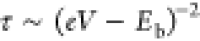 voltage scaling of the switching times
(see Supporting Information). The red and
blue dashed lines in Figure 4b illustrate the best fits with the former voltage scaling,
which is clearly inconsistent with the measured data. Even if the
divergence at eV = E is blurred
due to a broader energy distribution, the high bias 1/V scaling of this simple model is much shallower than the measured
voltage dependence of the data, which also holds for the 1/V2 scaling in the incoherent model. Note that
a 1/V and 1/V2 dependencies
would yield a factor of 3 or 9 speedup between 50 and 150 mV driving
in contrast to the observed ≈2 orders of magnitude speedup
(see Figure 4b). In Figure 4g,h this 3-fold and
9-fold speedup would relate to slope values of b ≈
– 5 V–1 and b ≈ –
10 V–1, which are also much shallower slopes than
the typically observed b ≈ – 30 to
– 20 V–1 values. Accordingly, these models
are excluded.
voltage scaling of the switching times
(see Supporting Information). The red and
blue dashed lines in Figure 4b illustrate the best fits with the former voltage scaling,
which is clearly inconsistent with the measured data. Even if the
divergence at eV = E is blurred
due to a broader energy distribution, the high bias 1/V scaling of this simple model is much shallower than the measured
voltage dependence of the data, which also holds for the 1/V2 scaling in the incoherent model. Note that
a 1/V and 1/V2 dependencies
would yield a factor of 3 or 9 speedup between 50 and 150 mV driving
in contrast to the observed ≈2 orders of magnitude speedup
(see Figure 4b). In Figure 4g,h this 3-fold and
9-fold speedup would relate to slope values of b ≈
– 5 V–1 and b ≈ –
10 V–1, which are also much shallower slopes than
the typically observed b ≈ – 30 to
– 20 V–1 values. Accordingly, these models
are excluded.
(ii) Temperature activated switching model. In
the former two-level system models the direct voltage excitation is
not possible at eV < E or eV < Eb voltage. In this
limit the temperature activation can still induce a transition with  or
or 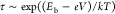 switching times (see Supporting Information). Such a temperature-activated process
is unrealistic at T = 4.2 K temperature, as the energy
scale in the numerator of the exponent is almost 3 orders of magnitude
larger than the thermal energy in the denominator. Furthermore, this
scaling would provide a slope of b = −e·log(e)/kT ≈
– 103 V–1, whereas the largest
measured slopes are restricted to b ≈ –
30 V–1 (see Figure 4g,h).
switching times (see Supporting Information). Such a temperature-activated process
is unrealistic at T = 4.2 K temperature, as the energy
scale in the numerator of the exponent is almost 3 orders of magnitude
larger than the thermal energy in the denominator. Furthermore, this
scaling would provide a slope of b = −e·log(e)/kT ≈
– 103 V–1, whereas the largest
measured slopes are restricted to b ≈ –
30 V–1 (see Figure 4g,h).
(iii) Vibrational pumping model. So far we have
considered models where the energy release from the electrons kicks
the molecule to its other state within a single event. Alternatively,
the electrons may release smaller E = ℏω vibrational quanta to the molecule, and the transition happens once
this vibrational degree of freedom is pumped35,36 to an energy exceeding the barrier height. According to the consideration
in the Supporting Information, the average
occupation number of a vibrational mode can be estimated as  . Considering the
  transmission probability
of the molecule,
the eV < 150 mV voltage range and ≈10–100
meV typical vibrational energies37
transmission probability
of the molecule,
the eV < 150 mV voltage range and ≈10–100
meV typical vibrational energies37 follows, i.e., the vibrational pumping,
and related local overheating of the junction is unrealistic. As a
simple explanation this result is related to the fact that the vibrational
mode is much more efficiently cooled than excited in the
follows, i.e., the vibrational pumping,
and related local overheating of the junction is unrealistic. As a
simple explanation this result is related to the fact that the vibrational
mode is much more efficiently cooled than excited in the  limit.
(iv) Double-well potential inversion model. Recent studies reported single-molecule switching, where the voltage excitation reversed the dominance of the two molecular states; i.e., it induced an inversion of the minima in the double-well potential12 (see the illustration in the Supporting Information). This was reflected by the clear crossing in the voltage dependence of the switching times. In our system the dominance of the states is manipulated by the displacement, but at a fixed electrode separation the switching of the two configurations speeds up simultaneously, and the initially dominant state remains dominant throughout the studied voltage train; i.e., the double-well potential inversion model is also excluded.
(v) Heuristic model relying on the molecule’s energy dependent transition probability. To be able to describe the simultaneous exponential decay of the switching times with linearly increasing voltage, we consider a strong (exponential) energy dependence of the molecule’s transition probability Γ(E) (see left illustration in Figure 5). This may relate to an energy dependent tunnelling probability between two conformational states, as implied on the figure, but several other processes, like the reduction of the barrier with the applied voltage, or the influence of electron-wind forces may play a role. A more detailed understanding of the precise microscopic processes would require first principle model calculations.
In conclusion, we have demonstrated well-controlled voltage-induced probabilistic conductance switching in cryogenic temperature Au–BP–Au single-molecule junctions. This behavior resembles probabilistic bit devices with two tunable parameters: the relative dominance of the two conductance states is manipulated by the electrode displacement, whereas the voltage manipulation induces an exponential speedup of both switching times.
We have compared our experimental results with possible model considerations and argued against simple two-level system models, temperature activated switching models, a vibrational pumping model, and a double-well potential inversion model. Finally, we proposed a heuristic model relying on the exponential energy dependence of the molecule’s transition probability.
Acknowledgments
This work was supported by the BME-Nanonotechnology FIKP grant of EMMI (BME FIKP-NAT) and the NKFI K119797 grant. The authors are thankful to K. P. Lauritzen and G. C. Solomon for the graphical illustration of the gold–BP–gold structures.
Supporting Information Available
The Supporting Information is available free of charge at https://pubs.acs.org/doi/10.1021/acs.jpclett.0c02185.
Discussion of the model considerations and details on the fitting of the switching time distributions (PDF)
Author Contributions
¶ G.M. and Z.B. contributed equally to this work
Author Contributions
The measurements were performed and analyzed by G. Mezei and Z. Balogh. The real-time-controlled measurement system was developed and programmed by A. Magyarkuti. The project was supervised by A. Halbritter. All authors contributed to the discussion and interpretation of the results. The manuscript was written by A. Halbritter, G. Mezei, and Z. Balogh with input from all authors.
The authors declare no competing financial interest.
Supplementary Material
References
- Cuevas J. C.; Scheer E. In Molecular Electronics: An introduction to Theory and Experiment; Reed M., Ed.; World Scientific: Singapore, 2010. [Google Scholar]
- Sun L.; Diaz-Fernandez Y. A.; Gschneidtner T. A.; Westerlund F.; Lara-Avila S.; Moth-Poulsen K. Single-molecule electronics: from chemical design to functional devices. Chem. Soc. Rev. 2014, 43, 7378–7411. 10.1039/C4CS00143E. [DOI] [PubMed] [Google Scholar]
- van der Molen S. J.; Liljeroth P. Charge transport through molecular switches. J. Phys.: Condens. Matter 2010, 22, 133001. 10.1088/0953-8984/22/13/133001. [DOI] [PubMed] [Google Scholar]
- Zhang J. L.; Zhong J. Q.; Lin J. D.; Hu W. P.; Wu K.; Xu G. Q.; Wee A. T. S.; Chen W. Towards single molecule switches. Chem. Soc. Rev. 2015, 44, 2998–3022. 10.1039/C4CS00377B. [DOI] [PubMed] [Google Scholar]
- Liu Z.; Ren S.; Guo X. Switching Effects in Molecular Electronic Devices. Topics in Current Chemistry 2017, 375, 56. 10.1007/s41061-017-0144-5. [DOI] [PubMed] [Google Scholar]
- Quek S. Y.; Kamenetska M.; Steigerwald M. L.; Choi H. J.; Louie S. G.; Hybertsen M. S.; Neaton J. B.; Venkataraman L. Mechanically controlled binary conductance switching of a single-molecule junction. Nat. Nanotechnol. 2009, 4, 230–234. 10.1038/nnano.2009.10. [DOI] [PubMed] [Google Scholar]
- Su T. A.; Li H.; Steigerwald M. L.; Venkataraman L.; Nuckolls C. Stereoelectronic switching in single-molecule junctions. Nat. Chem. 2015, 7, 215–220. 10.1038/nchem.2180. [DOI] [PubMed] [Google Scholar]
- Roldan D.; Kaliginedi V.; Cobo S.; Kolivoska V.; Bucher C.; Hong W.; Royal G.; Wandlowski T. Charge Transport in Photoswitchable Dimethyldihydropyrene-Type Single-Molecule Junctions. J. Am. Chem. Soc. 2013, 135, 5974–5977. 10.1021/ja401484j. [DOI] [PubMed] [Google Scholar]
- Sendler T.; Luka-Guth K.; Wieser M.; Lokamani; Wolf J.; Helm M.; Gemming S.; Kerbusch J.; Scheer E.; Huhn T.; et al. Light-Induced Switching of Tunable Single-Molecule Junctions. Advanced Science 2015, 2, 1500017. 10.1002/advs.201500017. [DOI] [PMC free article] [PubMed] [Google Scholar]
- Tam E. S.; Parks J. J.; Shum W. W.; Zhong Y.-W.; Santiago-Berríos M. B.; Zheng X.; Yang W.; Chan G. K.-L.; Abruña H. D.; Ralph D. C. Single-Molecule Conductance of Pyridine-Terminated Dithienylethene Switch Molecules. ACS Nano 2011, 5, 5115–5123. 10.1021/nn201199b. [DOI] [PubMed] [Google Scholar]
- Kim Y.; Hellmuth T. J.; Sysoiev D.; Pauly F.; Pietsch T.; Wolf J.; Erbe A.; Huhn T.; Groth U.; Steiner U. E.; et al. Charge Transport Characteristics of Diarylethene Photoswitching Single-Molecule Junctions. Nano Lett. 2012, 12, 3736–3742. 10.1021/nl3015523. [DOI] [PubMed] [Google Scholar]
- Meng L.; Xin N.; Hu C.; Wang J.; Gui B.; Shi J.; Wang C.; Shen C.; Zhang G.; Guo H.; et al. Side-group chemical gating via reversible optical and electric control in a single molecule transistor. Nat. Commun. 2019, 10, 1450. 10.1038/s41467-019-09120-1. [DOI] [PMC free article] [PubMed] [Google Scholar]
- Collier C. P.; Wong E. W.; Belohradský M.; Raymo F. M.; Stoddart J. F.; Kuekes P. J.; Williams R. S.; Heath J. R. Electronically Configurable Molecular-Based Logic Gates. Science 1999, 285, 391–394. 10.1126/science.285.5426.391. [DOI] [PubMed] [Google Scholar]
- Blum A. S.; Kushmerick J. G.; Long D. P.; Patterson C. H.; Yang J. C.; Henderson J. C.; Yao Y.; Tour J. M.; Shashidhar R.; Ratna B. R. Molecularly inherent voltage-controlled conductance switching. Nat. Mater. 2005, 4, 167–172. 10.1038/nmat1309. [DOI] [PubMed] [Google Scholar]
- Lörtscher E.; Ciszek J. W.; Tour J.; Riel H. Reversible and Controllable Switching of a Single-Molecule Junction. Small 2006, 2, 973–977. 10.1002/smll.200600101. [DOI] [PubMed] [Google Scholar]
- Schwarz F.; Kastlunger G.; Lissel F.; Egler-Lucas C.; Semenov S. N.; Venkatesan K.; Berke H.; Stadler R.; Lörtscher E. Field-induced conductance switching by charge-state alternation in organometallic single-molecule junctions. Nat. Nanotechnol. 2016, 11, 170–176. 10.1038/nnano.2015.255. [DOI] [PubMed] [Google Scholar]
- Schröder H. V.; Schalley C. A. Electrochemically switchable rotaxanes: recent strides in new directions. Chem. Sci. 2019, 10, 9626–9639. 10.1039/C9SC04118D. [DOI] [PMC free article] [PubMed] [Google Scholar]
- Fujii S.; Koike M.; Nishino T.; Shoji Y.; Suzuki T.; Fukushima T.; Kiguchi M. Electric-Field-Controllable Conductance Switching of an Overcrowded Ethylene Self-Assembled Monolayer. J. Am. Chem. Soc. 2019, 141, 18544–18550. 10.1021/jacs.9b09233. [DOI] [PubMed] [Google Scholar]
- Tang C.; Zheng J.; Ye Y.; Liu J.; Chen L.; Yan Z.; Chen Z.; Chen L.; Huang X.; Bai J.; et al. Electric-Field-Induced Connectivity Switching in Single-Molecule Junctions. iScience 2020, 23, 100770. 10.1016/j.isci.2019.100770. [DOI] [PMC free article] [PubMed] [Google Scholar]
- Kim T.; Darancet P.; Widawsky J. R.; Kotiuga M.; Quek S. Y.; Neaton J. B.; Venkataraman L. Determination of Energy Level Alignment and Coupling Strength in 4,4’-Bipyridine Single-Molecule Junctions. Nano Lett. 2014, 14, 794–798. 10.1021/nl404143v. [DOI] [PubMed] [Google Scholar]
- Aradhya S. V.; Frei M.; Hybertsen M. S.; Venkataraman L. Van der Waals interactions at metal/organic interfaces at the single-molecule level. Nat. Mater. 2012, 11, 872. 10.1038/nmat3403. [DOI] [PubMed] [Google Scholar]
- Borges A.; Fung E.-D.; Ng F.; Venkataraman L.; Solomon G. C. Probing the Conductance of the s-System of Bipyridine Using Destructive Interference. J. Phys. Chem. Lett. 2016, 7, 4825–4829. 10.1021/acs.jpclett.6b02494. [DOI] [PubMed] [Google Scholar]
- Magyarkuti A.; Lauritzen K. P.; Balogh Z.; Nyáry A.; Mészáros G.; Makk P.; Solomon G. C.; Halbritter A. Temporal correlations and structural memory effects in break junction measurements. J. Chem. Phys. 2017, 146, 092319. 10.1063/1.4975180. [DOI] [Google Scholar]
- Isshiki Y.; Fujii S.; Nishino T.; Kiguchi M. Impact of junction formation processes on single molecular conductance. Phys. Chem. Chem. Phys. 2018, 20, 7947–7952. 10.1039/C8CP00317C. [DOI] [PubMed] [Google Scholar]
- Magyarkuti A.; Balogh N.; Balogh Z.; Venkataraman L.; Halbritter A. Unsupervised feature recognition in single-molecule break junction data. Nanoscale 2020, 12, 8355–8363. 10.1039/D0NR00467G. [DOI] [PubMed] [Google Scholar]
- Camsari K. Y.; Sutton B. M.; Datta S. p-bits for probabilistic spin logic. Appl. Phys. Rev. 2019, 6, 011305. 10.1063/1.5055860. [DOI] [Google Scholar]
- Borders W. A.; Pervaiz A. Z.; Fukami S.; Camsari K. Y.; Ohno H.; Datta S. Integer factorization using stochastic magnetic tunnel junctions. Nature 2019, 573, 390–393. 10.1038/s41586-019-1557-9. [DOI] [PubMed] [Google Scholar]
- Yanson A. I.; Rubio Bollinger G.; van den Brom H. E.; Agraït N.; van Ruitenbeek J. M. Formation and manipulation of a metallic wire of single gold atoms. Nature 1998, 395, 783–785. 10.1038/27405. [DOI] [Google Scholar]
- Ohnishi H.; Kondo Y.; Takayanagi K. Quantized conductance through individual rows of suspended gold atoms. Nature 1998, 395, 780–785. 10.1038/27399. [DOI] [Google Scholar]
- Untiedt C.; Yanson A. I.; Grande R.; Rubio-Bollinger G.; Agraït N.; Vieira S.; van Ruitenbeek J. Calibration of the length of a chain of single gold atoms. Phys. Rev. B: Condens. Matter Mater. Phys. 2002, 66, 085418. 10.1103/PhysRevB.66.085418. [DOI] [Google Scholar]
- Trouwborst M. L.; Huisman E. H.; Bakker F. L.; van der Molen S. J.; van Wees B. J. Single Atom Adhesion in Optimized Gold Nanojunctions. Phys. Rev. Lett. 2008, 100, 175502. 10.1103/PhysRevLett.100.175502. [DOI] [PubMed] [Google Scholar]
- Aradhya S. V.; Nielsen A.; Hybertsen M. S.; Venkataraman L. Quantitative Bond Energetics in Atomic-Scale Junctions. ACS Nano 2014, 8, 7522–7530. 10.1021/nn502836e. [DOI] [PubMed] [Google Scholar]
- Halbritter A.; Borda L.; Zawadowski A. Slow two-level systems in point contacts. Adv. Phys. 2004, 53, 939–1010. 10.1080/00018730412331324981. [DOI] [Google Scholar]
- Halbritter A.; Makk P.; Csonka S.; Mihály G. Huge negative differential conductance in Au-H2 molecular nanojunctions. Phys. Rev. B: Condens. Matter Mater. Phys. 2008, 77, 075402. 10.1103/PhysRevB.77.075402. [DOI] [Google Scholar]
- Todorov T. N. Local heating in ballistic atomic-scale contacts. Philos. Mag. B 1998, 77, 965–973. 10.1080/13642819808206398. [DOI] [Google Scholar]
- Frederiksen T.; Paulsson M.; Brandbyge M.; Jauho A.-P. Inelastic transport theory from first principles: Methodology and application to nanoscale devices. Phys. Rev. B: Condens. Matter Mater. Phys. 2007, 75, 205413. 10.1103/PhysRevB.75.205413. [DOI] [Google Scholar]
- Kim Y.; Hellmuth T. J.; Bürkle M.; Pauly F.; Scheer E. Characteristics of Amine-Ended and Thiol-Ended Alkane Single-Molecule Junctions Revealed by Inelastic Electron Tunneling Spectroscopy. ACS Nano 2011, 5, 4104–4111. 10.1021/nn200759s. [DOI] [PubMed] [Google Scholar]
Associated Data
This section collects any data citations, data availability statements, or supplementary materials included in this article.