Abstract
Single-electron devices are capable of detecting changes of the electric field caused by the presence of one single electron in their environment. These devices are optimized to identify the material that is in close contact with them based on the material's internal charge distribution or dipole moment. As an important practical use, they present the possibility of detecting bacteria, viruses, or pathogens. However, their practical use is hampered by their nano-meter size, which is normally an order of magnitude smaller than that of detected species, their very complex fabrication techniques, their cryogenic operational temperature, and the problem of bringing the said species in contact with the single-electron structure. In this document, a large scaled room temperature single-electron structure is introduced, and its ability to distinguish liquids based on their internal dipole moments is demonstrated. The device is a Schottky junction made of PtSi, as the metal contact, and the walls and surfaces of the porous Si, as the semiconductor. The reverse bias current-voltage (IV) characteristic of this device is sensitive to 1 ppm change in the dipole moment of the liquid entering its pores. The simple fabrication, easy testing procedure, high sensitivity, and fast response can make this device an optimized testing kit to identify the given bacteria, viruses, or pathogens dissolved in liquids.
Keywords: Virus identification, Bacteria identification, Porous silicon, Liquid dielectric constant, Pathogen dipole moment, Single-electron effect
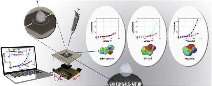
Graphical abstract
1. Introduction
The importance of the fast and reliable detection of biological agents such as cancerous cells, bacteria, and viruses is well understood. The early and fast diagnosis of viruses, for example, has become ever more pressing as pandemic breakouts have shown that the early detection and tracking are critical to prevent the spread of contagious diseases. To help in the same regard, electronic-based detectors can be of high importance if they can be programmed to detect novel or particular pathogens as needs arise. In this study, an electronic detection mechanism, known as single-electron effect, is proposed to detect and identify molecules dissolved in a liquid. To date, various methods for the identification of constituents of liquids, such as liquid chromatography [1,2] and microfluidics [[3], [4], [5], [6]], have been used. Normally in these methods molecules are separated and then detected using ultraviolet, photoluminescence, fluorescence, electrochemical, refractive index, and electrical conductivity tests and procedures. These methods are relatively complicated, expensive and time-consuming. The device introduced in this paper, beside being easy to fabricate, simple to use, and fast to respond, provides the most accurate measurements of the electrical properties of molecules. Although single-electron devices have existed for some time [7], they have not yet been practically used for this particular purpose due to three critical obstacles, which are mentioned below.
The single-electron effect provides the ability to manipulate electrons one by one either by transferring them from one part of a circuit to another or by storing them in a reservoir. The simplest single-electron device is a nano-sized particle connected, via tunnel barriers, to two connections from outside and is dubbed the single-electron “island”. The size of the island is normally about 10 nm, and its capacitance value is about 10−17 f [7]. Such a low capacitance implies that a relatively large threshold voltage of about 50 mV is needed to transfer one electron into this island [7]. The transfer of electrons from the connections into and out of the island happens one at a time and is only possible if the threshold voltage reaches the island across the connections. The electric fields around the island, or the dielectric constants of the surrounding material, change the threshold voltage and create the mechanism for detection. It has been shown that the depletion capacitor of a Schottky junction can exhibit single-electron effect as well [8]. In this case, only the reverse bias IV curve of the junction manifests the single-electron effect, and in the forward bias mode the thermionic current shorts out the depletion capacitor with very small resistance and overrides the single-electron effect. It is possible to increase the size of the device considerably if the porous Si is used as the semiconductor part of the Schottky junction [8].
Since its discovery, the porous Si has been the subject of much research because of its large surface area as well as its unprecedented electrical [9,10], optical [11,12], and mechanical [13,14] properties and also its compatibility with silicon-based microelectronic devices [15]. Some of its applications include being used in areas such as optoelectronics [16], micromachines (as sacrificial layers) [17], and sensors (like for detecting gas [18,19], proteins [20], DNA [21], organic solvents [22,23], bacteria [24,25] and viruses [26]). Here, the electric fields, created by the sharp and needle-like pores, help to produce the single-electron effect. Platinum silicide (PtSi) is used as the metal contact because of its ease of formation and its well-characterization, reproducibility, and uniformity [27].
There are three practical problems with the realization of the single-electron device as pathogen detector. First, it is the size of the island [28], which is less than the sizes of the cells, viruses, and bacteria. This creates a problem because their alignment, with respect to the island, affects the measurements unpredictably. Second, the threshold voltage is normally less than 100 mV, and as a result, they need to be cooled to cryogenic temperatures to overcome thermal noises. Third, the detected species must be brought to close proximity of the island, which can only be accomplished in a liquid solution. Liquid solutions, however, can short out the two connections.
In this paper, experimental results for the realization of a large scaled single-electron liquid detector operating at the room temperature are presented. It is demonstrated that it can distinguish and identify various liquids based on their dipole moments [29]. It is shown that by changing the dipole moment, the IV characteristics changes consistently as well. The response time of the device to the change of liquid is around 30 s and is limited by the circuitry that obtains the IV curve. Experimental results demonstrate that this device is quite sensitive to the changes in the dipole moment of the liquids, and considering the noise of the circuit used, a change of 1 ppm in the dipole moment can be detected. This means that dissolved viruses, bacteria, or pathogens can be distinguished with great precision and accuracy.
2. Experimental procedure
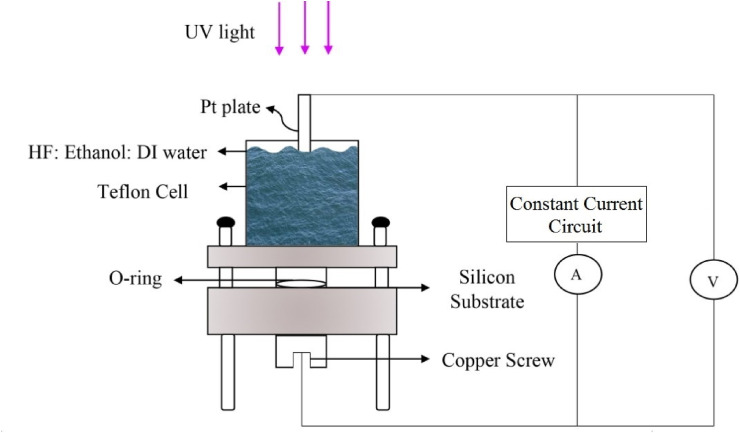
N-type Si wafers with the resistivity of 1–10 Ωcm are made porous through the anodic etching having used the hydrofluoric acid (HF) solution of which the concentration, applied voltage, duration, and temperature determine the level of porosity. A wealth of literature exists on obtaining consistent and reproducible pores with various openings, widths, and depths [[30], [31], [32]]. The characteristics of Si wafers and parameters related to etching conditions are provided in Table 1 . Table 1 also includes the parameters related to the Pt deposition, which occurs right after etching by running DI water over the etching acid till it is completely removed and then adding the solution for electrodepositing Pt. It has been previously shown that Pt enters the pores and starts to fill them from the bottom to the top [8]. The equipment used for etching and subsequently depositing Pt is shown in Fig. 1 . The whole process is performed in a chemical lab under a chemical hood equipped with the regular ventilation for acid vapors.
Table 1.
Characteristics of the Si wafer, and Si etching and Pt deposition parameters.
| Silicon type | Resistivity (Ωcm) | Crystalline orientation | Dopant | Thickness (μm) | |
| n-type | 1–10 | <100> | Phosphorus | 525 ∓ 25 | |
| Process | Solution (%) | Current density (mA cm−2) | Time (min) | Temperature (°C) | |
| Si etchinga | 38% HF 99% DI water 99% Ethanol |
25 25 50 |
21.50 | 23 | 20 |
| Process | Solution (g L−1) | Current density (mA cm−2) | Time (min) | Temperature (°C) | |
| Pt deposition | H2(PtCl6)·6H2O (NH4)2HPO4 Na2HPO4 |
4 20 100 |
9.62 | 45 | 70 |
Si etching was performed under the ultraviolet light and in an ultrasonic bath.
Fig. 1.
The apparatus, with which both the anodic etching and Pt electrodeposition are performed, is made of a Teflon cell with two separate parts. The bottom consists of a Cu disc, which makes contact with the bottom side of the Si sample. Si is pressed against this disc by the screws that push the top Teflon part down to the bottom. An O-ring is placed on the Si sample and the pressure by the top Teflon part prevents the etching solution from leaking outside. The solution is poured inside a funnel in the top cell and makes contact with the Si bordered by the O-ring. The funnel is large enough to allow ultraviolet light to reach Si from the top. Etching is performed while the whole set up is suspended in an ultrasonic bath. Immediately after etching, the solution is washed out and a new solution for the electrodeposition of Pt is poured in. The electrodeposition is performed in the same cell.
The Pt/porous Si junction is hence created but such a junction is not reproducible or reliable due to surface states at the Pt and Si interface. To solve this problem the whole structure is annealed under a vacuum at 400 °C [27]. This causes Pt to react with Si and create the PtSi alloy. The final Schottky junction is made of PtSi and the porous surface of Si. The interesting consequence, which makes this junction reproducible, is the fact that PtSi is created by the diffusion of Pt into the Si layer. The electrical junction between PtSi and Si occurs inside and below the initial Si surface, and as a result, is not affected by the impurities or surface states of the Si top layer.
After the creation of PtSi, the whole structure is put in an etching solution to completely empty the pores from the remaining Pt. This process takes about 5 min. Connections to Si as well as PtSi, which has covered the porous area, are made via a silver paste. Silver paste creates an ohmic contact to Si, and since PtSi is a metal alloy, a low loss connection is created on it as well. The contact resistance to both PtSi and Si was measured via a four-point probe and was estimated to be below 1 mΩ [8,33].
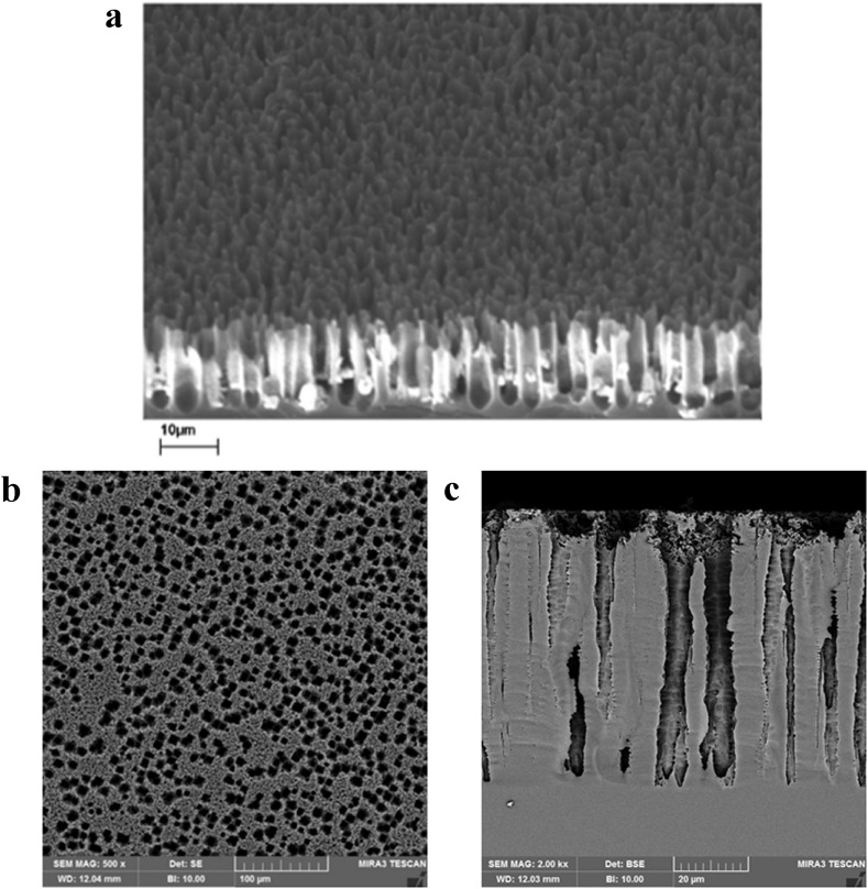
Conditions given in Table 1 produce porous samples with circular pore openings of about 2–3 μm in diameter and the depth of about 10 μm, while being surrounded by larger and deeper pores. The SEM micrographs of representative samples are provided in Fig. 2 . The porous sample of Fig. 2a shows the pores and the PtSi covering their sidewalls. This porosity level was proven to exhibit the single-electron effect at the room temperature [8] and also this structure has been successfully tested as a gas and IR detector based on the same underlying phenomenon of the single-electron effect [[33], [34], [35]]. The gas detection and the liquid detection are identical in the fact that the material filling the pores changes the IV curve based on its dipole moment. Such porosity level exhibits a threshold voltage of about −10 V [8,[33], [34], [35]]. For the liquid detection, it might be more appropriate to create pores with larger openings to help liquids enter the pores. The porous samples shown in Fig. 2b and c were used in experiments provided in this report. As it is seen, there are openings of about 10 μm surrounding pores with openings of about 2 μm. Fig. 2c shows the depth of these pores, which reaches about 70 μm into the semiconductor. These samples exhibit a threshold voltage of about −20 V. The porous Si with other porosity levels and pore characteristics can be used as long as they exhibit single-electron effect. Perhaps the size and shape of detected species could dictate the final porosity structure.
Fig. 2.
(a) SEM micrograph of a typical PtSi/Porous Si sample. The white areas at the walls of the pores are PtSi. As it can be seen, the pore openings are a few μm wide and their depth is about 10 μm. The porosity at the scale of the device is uniform and reproducible as witnessed in reproducible IV characteristics. Liquid enters the pores and makes contact with the PtSi covering the sidewalls. The PtSi layer creates the bright white areas seen in the graph. (b) The porous samples of which results are provided in this paper. Porosity is such that pores with a diameter of 10 μm are surrounding pores similarly to Fig. 1a. (c) The depth of the large pores reach down to 70 μm. This porosity has been used to help liquids with higher surface tension to enter the pores as well.
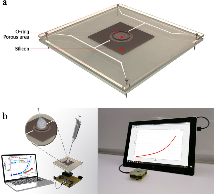
Fig. 3 demonstrates the experimental setup. An O-ring is placed over the porous area where liquid is to be poured. Two printed circuit boards sandwich the sample and are pushed toward one another via four screws. They press the O-ring against the porous surface, and at the same time, make contact with both Si and PtSi. Two contacts are fed into a circuit, which is situated underneath the sample and obtains the IV curve by applying the voltage, at the minimum value of 1 mV, and reading the current. The results are sent to a computer and displayed. The electrical power delivered to the sample for obtaining the IV curve is low enough to be supplied by the USB connection of a computer. Therefore, the electrical circuit only needs a computer to power it up. The USB voltage can be boosted up to as large as 50 V by the designed circuit if needed.
Fig. 3.
The whole device and measurement set up is presented here. The sample and its connections are shown schematically here because the actual unit, given in Fig. b, is opaque and the details cannot be seen. Two printed circuit boards push on an O-ring and sandwich the sample. Only the porous area is exposed to the liquid that is poured into the opening. The O-ring prevents the liquid from reaching other parts of the sample. Connections to the porous area and Si itself happen by pressing Ag terminals on the contacts to these areas via Silver paste. The sample holder is inserted into the measuring circuit that sends current into the device and measures its voltage. The result is sent to a computer of which the USB port is used to power the circuit itself.
The porous area is about 2 cm2, and the O-ring covers its inside borders exposing only about 1 cm2 of the porous surface to the liquid. The O-ring prevents the leakage and penetration of liquid underneath and into the Si side surrounding the porous area. As it was mentioned before, only the reverse bias IV curve exhibits the single-electron effect, which manifests itself as a relatively small current, at the voltage values below the threshold voltage, but it increases drastically afterwards. The relatively small current below the threshold voltage is also an order of magnitude less than what is observed in regular PtSi/Si Schottky junctions of the same size [8,34]. Regular samples not only exhibit remarkably larger currents in reverse bias, but also are not sensitive to IR, gases [8,34,36], and liquids.
The fact that a large scaled sample is able to provide a small enough capacitor to exhibit the single-electron effect at the room temperature is explained as follows [8]. The value of the capacitance is obtained by calculating the electric field, created by one electron around a structure, and then integrating it over the distance to infinity. This provides the energy necessary for transferring an electron to the structure, which is the inverse of capacitance. Consequently, a larger electric field around a structure should result in a larger voltage and a smaller capacitance. The sharp edges of the porous surface can be likened to needle-like structures. As it is known, the electric field around sharp objects such as needles can increase by an order of magnitude compared to the fields created by the same charges over a plane surface. These large electric fields are exactly the reason why porous surfaces provide the capacitance reduced by an order of magnitude. They are also responsible for creating a very narrow Schottky barrier allowing electrons to tunnel from PtSi into Si. In effect, electrons do not see the Schottky potential barrier, and the only barrier they have to surmount is the single-electron barrier, which is manifested as the threshold voltage.
There are two equivalent ways of explaining the gas and liquid detection by the PtSi/porous Si junction. One is to consider that molecules, which come in contact with PtSi walls, attract charges to the upper surface of PtSi due to their dipole moment. The larger the dipole moment of the material, the larger the charge transferred to the PtSi layer. This redistributes charges on the metallic layer, which in turn affects charges inside the semiconductor, and therefore affects the capacitance. The other equivalent point of view is to consider the liquid as the medium or dielectric of a parasitic capacitor between the PtSi surface and the ground. The total capacitance of the device is a combination of this capacitance and the depletion capacitance. Therefore, when gas or liquid is changed so is the capacitor from the device to the ground, and so are the effective capacitance electrons see in charging the depletion capacitor. A change in the effective capacitance changes the threshold voltage and hence the IV characteristics. How much of a change this device can sense depends mostly on the circuit noise because theoretically, a single-electron device is sensitive to changes of one single electron in its vicinity. In this report, the detected 1 ppm of change in the dipole moment is demonstrated.
3. Results and discussion
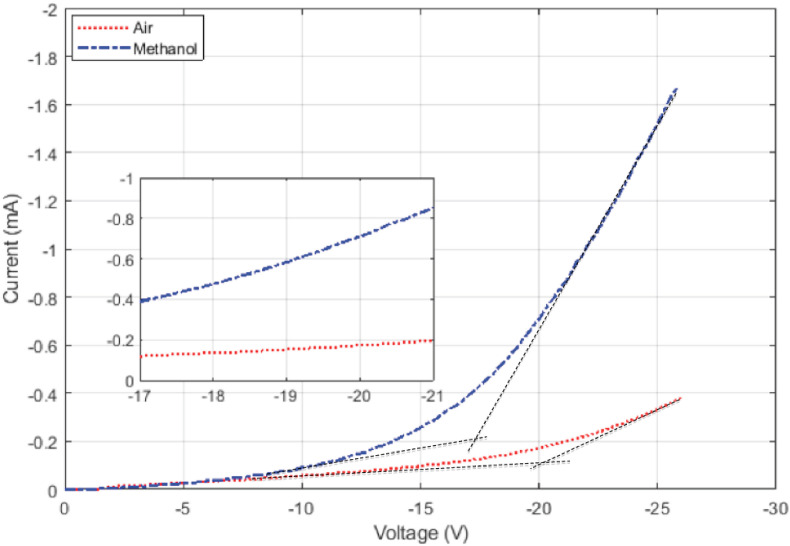
Fig. 4 shows the experimental IV curves of the sample when in air and when methanol has filled the pores (the negative values denote the reverse bias mode). The zero current at very low voltage values is an artifact of the digital IV curve sampling, which has rounded off values to zero. Two distinct portions with different slopes are distinguishable in each IV curve. When two line asymptotes are fitted to each graph, their intersection can be considered roughly as the threshold voltage for the single-electron transfer. The accurate measurement is carried out by analyzing the IV curve numerically and determining when the IV curve changes from an exponential to a pure power-law curve. This is because the current below the threshold voltage is caused by energetic electrons that can surmount the single-electron barrier (the threshold voltage) and, like in all such cases, it follows the Fermi-Dirac distribution and density of states of electrons in the metal (which is constant for the voltage ranges used here) and results in an exponential IV curve. The seemingly crude method of asymptotic lines matches the numerically obtained one quite well but normally overestimates it by about 1 V. Doing this, the threshold voltage for the device in air is estimated as about −20.5 V, and in methanol as about −17 V. The exact value of the threshold voltage is not critical because, as will be discussed later, the entire IV curve is used to identify a liquid.
Fig. 4.
Room-temperature reverse bias I–V curves of a PtSi/Porous Si junction in the air and when it is in contact with methanol. There is a remarkable difference in the IV curves. The threshold voltage for the single-electron transfer can be estimated by drawing two asymptotes to the curves, one at low and one at high voltages. Their intersection is a rough indication of the threshold voltage. In this case, the threshold voltage of the air has changed from −20.5 V to about −17 V for methanol. Notice that at the voltage of about −20 V the current has increased by about 0.3 mA from the air to methanol.
The difference between these two graphs is quite clear and demonstrates that this device can distinguish liquids unambiguously. Methanol has the largest relative permittivity amongst the alcohols used in experiments and has a value of 33 [37]. The relative permittivity, dielectric constant, and dipole moment reflect the same electrical characteristics. The relative permittivity or dielectric constant is used for solids and liquids, but when talking about individual molecules and atoms the dipole moment is used. It is dipole moments of molecules and their alignment that give rise to the specific relative permittivity or dielectric constant of a solid.
Although the dipole moment has the highest effect on the IV curve, there are other parameters that affect the IV curve as well. As it is seen in Fig. 4 and as will become apparent in subsequent figures, a liquid not only changes the threshold voltage, but also changes the slope of the IV curve after the threshold voltage. In experiments with the gas detection, a change in the gas content never changes the slope of the IV curve after the threshold [8,33,36]. Furthermore, while a decrease in the threshold voltage must be accompanied by a consistent increase in current at all voltage values, liquids do not follow this trend. For some of them, the current decreases at voltage values below half the threshold voltage. The change of slope and the decrease of the current at a low voltage are assumed to be related to the liquid's electron affinity and its electrical resistance but are subject to investigation. These two effects are not covered here, but even though they seem to complicate the analysis, they have been proved helpful in the reliable identification of liquids and their constituents. This is so because, if only dipole moments were to affect the IV curve, it would be conceivable that two liquids having different constituents would have the same dipole moment. But two liquids are less likely to be the same in dipole moment, resistivity and electron affinity. This also means that the entirety of a liquid's IV curve could be used as its fingerprint.
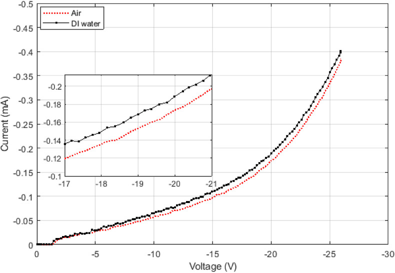
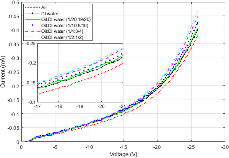
On the other hand, the surface tension can completely override the effects of the dipole moment by preventing the liquid from entering the pores. DI water has a relative permittivity twice as much as methanol does, but it does not decrease the threshold voltage as it is supposed to. Fig. 5 shows the corresponding IV curve of DI water and a device in the air. The change in threshold voltage is very small compared to that of methanol. To see whether the surface tension is actually playing a role here, a relatively non-polar oil with the dielectric constant of 3 was added to DI water to change its surface tension without much affecting its permittivity. The result for various concentrations of the oil is provided in Fig. 6 . The oil by itself affects the IV curve much less than DI water does. As the oil is added to DI water, the solution's dipole moment decreases, and the threshold voltage should increase. But IV curve changes in the opposite direction, and its threshold voltage decreases. It indicates that the oil is helping DI water enter the pores and more affect the IV curve by decreasing the surface tension.
Fig. 5.
DI water has a relative permittivity as about twice as methanol does but its IV curve does not change as much compared to that of methanol. The threshold voltage has decreased only by about half a volt compared to the threshold voltage of methanol changed by about 3.5 V as compared to the air (Fig. 4). This is due to the surface tension of water, which prevents it from completely entering the pores.
Fig. 6.
The IV curves of DI water when a relatively nonpolar oil has been added to change its surface tension while decreasing its permittivity only slightly. As it can be seen, by increasing the oil concentration the IV curve moves to left indicating the effect of DI water is felt more by the device. Put differently, water has been able to enter the pores and change the IV curve although the permittivity of the solution has decreased by the addition of the oil. The IV curve when only oil is poured on the sample does not change much compared to other liquids.
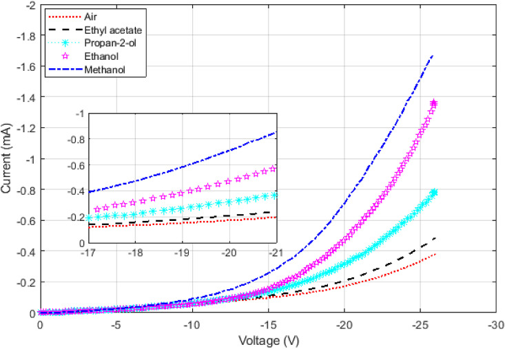
In Fig. 7 results for alcohols with different dipole moments are shown. Each result has a different IV curve based on its dipole moment. The distinguishing factor between them is not just the threshold voltage, but also the plurality of their IV curves; therefore, obtaining the exact threshold voltage is not needed for the practical usage. The threshold voltage is used as a rough estimate for the analytical reasoning and to test existing theories.
Fig. 7.
This diagram illustrates IV curves for the air and some alcohols of different permittivity such as methanol, ethanol, propan-2-ol, and ethyl acetate. The change in the IV curve follows the change in their dipole moments. The point to notice is the change in slope after the threshold voltage. The change in the slope is due to other factors besides the dipole moment that later can be used to better identify a liquid.
So far it has been demonstrated that liquids can have their own identifying IV curves but the most important factor determining their characteristics is their dipole moments. Regular methods of measuring dipole moments of materials and specifically liquids are rather complex and involve the measurement of the capacitance of a structure in which the liquid is its dielectric. This involves using ac inputs of up to several GHz, which also include impedance matching circuits in their input and output, for practical applications [38]. The sample preparation is time-consuming, and measurement apparatus are bulky and expensive. The accuracy of measurements is also highly dependent on the mismatch of the electrical connections at such frequencies [39]. The PtSi/porous Si device is much easier and cheaper to set up because measurements are done with dc signals, and the sample preparation is as simple as pouring the liquid on the device. Its sensitivity and accuracy are only limited to the noise and the sensitivity of the measurement circuit and its whole process takes about 30 s.
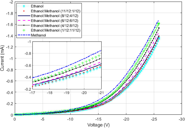
To demonstrate, that an incremental change in the dipole moment of the solution causes a corresponding change in the IV curve in a continuous fashion, Fig. 8 is provided. Methanol was added to ethanol in small amounts. The solution's relative permittivity increased gradually from that of ethanol (25.3) to the methanol's (33) [37] and IV curves were obtained for each case. The results for selected concentrations are provided and showing that a consistent change in the IV curve is created as the concentration of the solution increases. The smallest increase in current that can be detected is limited to the current noise. Assuming a relatively large current noise of about 60 nA for the circuit, a sensitivity of about 1 ppm can be obtained. This is so because, as Fig. 7, Fig. 8 show, around the voltage value of −20 V the current changes by 0.3 mA from ethanol to methanol, which only differ by 0.5% in their dipole moments. In other words, if the dipole moment changes by 1 ppm, it will cause at least 60 nA of current which is the minimum detectable change.
Fig. 8.
These results demonstrate that a continuous change in the dipole moment creates a corresponding continuous change in the IV curve. Methanol was added to ethanol in very small amounts to continuously change its dipole moment. A corresponding change in the IV curve was observed. The limit is the noise of the circuit. Some representative graphs are provided in this figure. A noise of 60 nA in the circuit results in the detection of a 1 ppm change in the relative permittivity.
To use this device for identifying pathogens, viruses and bacteria must be dissolved in a standard liquid with a known concentration and their IV curves obtained and tabulated. The IV curve of the unknown pathogen is compared to stored data for identification. A difference of 1 ppm in the dipole moment of pathogens is identifiable for a current noise of 60 nA. The entire process only takes a few minutes and needs only a small amount of the pathogen because the droplet of liquid used in the experiment is less than one-tenth of a milliliter. The device is ready to be used again as soon as it is removed from the circuit, cleaned and dried, which take only about 10 min.
4. Conclusions
Distinguishing liquids based on their dipole moments can be made simple and practical using PtSi/Porous Si Schottky junctions. The PtSi/Porous Si Schottky junction operates based on the single-electron effect and its sensitivity to changes in the dipole moment is only limited by the circuit noise, and therefore for a current noise of 60 nA, a sensitivity of one part per million was successfully achieved. Every pathogen dissolved in a standard liquid would have its own IV characteristics, which could be benchmarked for further identification. A difference of 1 ppm in the dipole moment results in an identifiable change in the IV curve. Measurement and identification take only a couple of minutes with a circuit powered by the USB port of any computer, and the device is ready for subsequent testing after a wash and subsequent dry.
Credit author statement
Shiva Ashoori fabricated the samples, performed the experiments and analyzed the results and helped in writing the paper. Maryam Naderpour fabricated the samples and performed the experiments. Mohammad M. Ghezelayagh made the equipment setup, obtained SEMs and helped with the measurement circuit design and fabrication. Reza Malekabadi Zadeh designed and built the circuit and wrote the computer program. Farshid Raissi came up with the idea, analyzed the results and helped write the paper.
Declaration of competing interest
The authors declare that they have no known competing financial interests or personal relationships that could have appeared to influence the work reported in this paper.
References
- 1.Önal A., Tekkeli S.E.K., Önal C. Review of the liquid chromatographic methods for the determination of biogenic amines in foods. Food Chem. 2013;138:509–515. doi: 10.1016/j.foodchem.2012.10.056. [DOI] [PubMed] [Google Scholar]
- 2.Rodriguez-Gomez R., Vandeput M., Zafra-Gomez A., Kauffmann J.M. Liquid chromatography-electrochemical detection for the determination of ethoxyquin and its dimer in pear skin and salmon samples. Talanta. 2018;177:157–162. doi: 10.1016/j.talanta.2017.08.078. [DOI] [PubMed] [Google Scholar]
- 3.Zheng Z., Wu L., Li L., Zong S., Wang Z., Cui Y. Simultaneous and highly sensitive detection of multiple breast cancer biomarkers in real samples using a SERS microfluidic chip. Talanta. 2018;188:507–515. doi: 10.1016/j.talanta.2018.06.013. [DOI] [PubMed] [Google Scholar]
- 4.Luka G., Ahmadi A., Najjaran H., Alocilja E., DeRosa M., Wolthers K., Malki A., Aziz H., Althani A., Hoorfar M. Microfluidics integrated biosensors: a leading technology towards lab-on-a-chip and sensing applications. Sensors. 2015;15:30011–30031. doi: 10.3390/s151229783. [DOI] [PMC free article] [PubMed] [Google Scholar]
- 5.Wang C.H., Chang C.J., Wu J.J., Lee G.B. An integrated microfluidic device utilizing vancomycin conjugated magnetic beads and nanogold-labeled specific nucleotide probes for rapid pathogen diagnosis. Nanomedicine: NBM (NMR Biomed.) 2014;10:809–818. doi: 10.1016/j.nano.2013.10.013. [DOI] [PubMed] [Google Scholar]
- 6.Chang W.H., Yang S.Y., Lin C.L., Wang C.H., Li P.C., Chen T.Y., Jan F.J., Lee G.B. Detection of viruses directly from the fresh leaves of a Phalaenopsis orchid using a microfluidic system. Nanomedicine: NBM (NMR Biomed.) 2013;9:1274–1282. doi: 10.1016/j.nano.2013.05.016. [DOI] [PubMed] [Google Scholar]
- 7.Likharev K.K. Single-electron devices and their applications. Proc. IEEE. 1999;87:606–632. [Google Scholar]
- 8.Raissi F., Abrishamian M.S., Emadi T. Single-electron effect in PtSi/Porous Si Schottky junctions. IEEE Trans. Electron. Dev. 2004;51:339–344. [Google Scholar]
- 9.Anderson R.C., Muller R.S., Tobias C.W. Investigations of the electrical properties of porous silicon. J. Electrochem. Soc. 1991;138:3406–3411. [Google Scholar]
- 10.Koyama H., Koshida N. Electrical properties of luminescent porous silicon. J. Lumin. 1993;57:293–299. [Google Scholar]
- 11.Theiß W. Optical properties of porous silicon. Surf. Sci. Rep. 1997;29:91–192. [Google Scholar]
- 12.Lockwood D.J. Optical properties of porous silicon. Solid State Commun. 1994;92:101–112. [Google Scholar]
- 13.Populaire C., Remaki B., Lysenko V., Barbier D., Artmann H., Pennek T. On mechanical properties of nanostructured meso-porous silicon. Appl. Phys. Lett. 2003;83:1370–1372. [Google Scholar]
- 14.Fakiri S., Montagne A., Rahmoun K., Iost A., Ziouche K. Mechanical properties of porous silicon and oxidized porous silicon by nanoindentation technique, Mat. Sci. Eng. A. 2018;711:470–475. [Google Scholar]
- 15.Barillaro G., Bruschi P., Pieri F., Strambini L.M. CMOS-compatible fabrication of porous silicon gas sensors and their readout electronics on the same chip. Phys. Status Solidi. 2007;204:1423–1428. [Google Scholar]
- 16.Herino R. Porous silicon for microelectronics and optoelectronics. Mater. Sci. Technol. 1997;13:965–970. [Google Scholar]
- 17.Bell T.E., Gennissen P.T.J., DeMunter D., Kuhl M. Porous silicon as a sacrificial material. J. Micromech. Microeng. 1996;6:361. [Google Scholar]
- 18.Ibraimov M.K., Sagidolda Y., Rumyantsev S.L., Zhanabaev Z.Z., Shur M.S. Selective gas sensor using porous silicon. Sens. Lett. 2016;14:588–591. [Google Scholar]
- 19.Ozdemir S., Gole J.L. The potential of porous silicon gas sensors. Curr. Opin. Solid ST. M. J. 2007;11:92–100. [Google Scholar]
- 20.Urmann K., Reich P., Walter J.G., Beckmann D., Segal E., Scheper T. Rapid and label-free detection of protein a by aptamer-tethered porous silicon nanostructures. J. Biotechnol. 2017;57:171–177. doi: 10.1016/j.jbiotec.2017.01.005. [DOI] [PubMed] [Google Scholar]
- 21.Di Francia G., La Ferrara V., Manzo S., Chiavarini S. Towards a label-free optical porous silicon DNA sensor. Biosens. Bioelectron. 2005;21:661–665. doi: 10.1016/j.bios.2004.12.008. [DOI] [PubMed] [Google Scholar]
- 22.Archer M., Christophersen M., Fauchet P.M. Electrical porous silicon chemical sensor for detection of organic solvents. Sens. Actuators B-Chem. 2005;106:347–357. [Google Scholar]
- 23.Klyui N.I., Ivanov I.I., Kyslovets O.S., Avksentyeva L.V., Skryshevsky V.A. Features of the use of optical reflection from thin porous silicon for detection of organic liquids. Sens. Actuators B-Chem. 2017;242:1177–1185. [Google Scholar]
- 24.Mathew F.P., Alocilja E.C. Porous silicon-based biosensor for pathogen detection. Biosens. Bioelectron. 2005;20:1656–1661. doi: 10.1016/j.bios.2004.08.006. [DOI] [PubMed] [Google Scholar]
- 25.Tang Y., Li Z., Luo Q., Liu J., Wu J. Bacteria detection based on its blockage effect on silicon nanopore array. Biosens. Bioelectron. 2016;79:715–720. doi: 10.1016/j.bios.2015.12.109. [DOI] [PubMed] [Google Scholar]
- 26.Rossi A.M., Wang L., Reipa V., Murphy T.E. Porous silicon biosensor for detection of viruses. Biosens. Bioelectron. 2007;23:741–745. doi: 10.1016/j.bios.2007.06.004. [DOI] [PubMed] [Google Scholar]
- 27.Dimitriadis C.A. Effect of conventional and rapid thermal annealing on platinum silicide Schottky barrier diodes. Appl. Phys. Lett. 1990;56:143–145. [Google Scholar]
- 28.Likharev K.K. Correlated discrete transfer of single electrons in ultrasmall tunnel junctions. IBM J. Res. Dev. 1988;32:144–158. [Google Scholar]
- 29.F. Raissi, Electronic Device for Detection of Viruses, Bacteria, and Pathogens, U.S. Patent 15 398 644, 2017.
- 30.Kleimann P., Linnros J., Petersson S. Formation of wide and deep pores in silicon by electrochemical etching. Mater. Sci. Eng., B. 2000;69:29–33. [Google Scholar]
- 31.Föll H., Christophersen M., Carstensen J., Hasse G. Formation and application of porous silicon. Mater. Sci. Eng. R Rep. 2002;39:93–141. [Google Scholar]
- 32.Kopani M., Mikula M., Kosnac D., Kovac J., Trnka M., Gregus J., Jerigova M., Jergel M., Vavrinsky E., Bacova S., Zitto P. Effect of etching time in hydrofluoric acid on the structure and morphology of n-type porous silicon. Appl. Surf. Sci. 2020:147463. [Google Scholar]
- 33.Raissi F., Farivar R. Room-temperature hydrogen gas sensor. Appl. Phys. Lett. 2005;87:164101. [Google Scholar]
- 34.Raissi F., Far M.M. Highly sensitive PtSi/Porous Si Schottky detectors. IEEE Sensor. J. 2002;2:476–481. [Google Scholar]
- 35.Raissi F., Sheeni N.A. Highly sensitive near IR detectors using n-type porous Si. Sens. Actuator A Phys. 2003;104:117–120. [Google Scholar]
- 36.Raissi F., Mirzakuchaki S., Jalili H.M., Erfanian A. Room-temperature gas-sensing ability of PtSi/Porous Si Schottky junctions. IEEE Sensor. J. 2006;6:146–150. [Google Scholar]
- 37.Lide D.R. 84th ed. CRC Press; 2003. CRC Handbook of Chemistry and Physics. [Google Scholar]
- 38.Maridevarmath C.V., Malimath G.H. Computational and experimental studies on dielectric relaxation and dipole moment of some anilines and phenol. J. Mol. Liq. 2017;241:845–851. [Google Scholar]
- 39.Gregory A.P., Clarke R.N. A review of RF and microwave techniques for dielectric measurements on polar liquids. IEEE Trans. Dielectr. Electr. Insul. 2006;13:727–743. [Google Scholar]


