

Abstract
In vivo, chronic neural recording is critical to understand the nervous system, while a tetherless, miniaturized recording unit can render such recording minimally invasive. We present a tetherless, injectable micro-scale opto-electronically transduced electrode (MOTE) that is ~60μm × 30μm × 330μm, the smallest neural recording unit to date. The MOTE consists of an AlGaAs micro-scale light emitting diode (μLED) heterogeneously integrated on top of conventional 180nm complementary metal-oxide-semiconductor (CMOS) circuit. The MOTE combines the merits of optics (AlGaAs μLED for power and data uplink), and of electronics (CMOS for signal amplification and encoding). The optical powering and communication enable the extreme scaling while the electrical circuits provide a high temporal resolution (<100μs). This paper elaborates on the heterogeneous integration in MOTEs, a topic that has been touted without much demonstration on feasibility or scalability. Based on photolithography, we demonstrate how to build heterogenous systems that are scalable as well as biologically stable – the MOTEs can function in saline water for more than six months, and in a mouse brain for two months (and counting). We also present handling/insertion techniques for users (i.e. biologists) to deploy MOTEs with little or no extra training.
Keywords: CMOS post processing, electrophysiology, heterogenous integration, physiological monitoring, tetherless neural recording
I. Introduction
CHRONIC neural recording is crucial in gaining a better understanding of the brain and could provide insights in neurological disorders such as Alzheimer’s Disease [1]. Although multi-electrode shanks are widely employed [2]–[4], they tend to generate ongoing damage and irritation due to relative motion between the implant and surrounding tissue [5]. Therefore, recent efforts have focused on building micro-scale, tetherless implants. While microscale RF [6]–[8] and ultrasonic [9]–[11] systems have shown promise, their transduction mechanisms make scaling below a millimeter challenging. On the other extreme, optical imaging based on calcium/voltage sensitive dyes/proteins allows noninvasive imaging at cell-scale resolution [1]. However, such optical imaging is limited by genetics to certain neurons and species, is impeded by scattering, and has a low temporal resolution. We present tetherless, injectable micro-scale optoelectronically transduced electrodes (MOTEs) which combine the merits of optical and electronic modalities to enable a) extreme scaling down to 60μm in cross-sectional diameter and b) direct electrical measurement with a high temporal resolution (<100μs). While circuit aspects of MOTEs have been present before [12], the challenges associated with heterogeneous integration and encapsulation are also significant in developing MOTEs, and are discussed here.
II. Theory
Heating in the brain dictates the maximum available optical power, where we have chosen infrared (IR) based on photovoltaic (PV) efficiency and minimal absorption in the brain. Reference [13] has shown 160mW/mm2 at the IR range to be the damage threshold. Our previous work has shown [12], [14] that a MOTE can function on a few microwatts of delivered power, so that it can function few millimeters deep in the brain through a transcranial window without exceeding 160mW/mm2. The same work has shown that it is possible to build a circuit that can provide > 10KHz bandwidth and ~15μVRMS noise floor, using pulse-position-modulation (PPM) encoding, often used in energy starved systems such as satellites [15].
Fig. 1 shows a proof-of-concept illustration of the MOTE. The proposed system comprises of two parts: a) an optical component, a micro-scale (μ) AlGaAs diode that acts as both a PV for power transfer and as a light emitting diode (LED) for data communication (hence often referred as PVLED [16], [17]), and b) an electrical component, a complementary metal-oxide-semiconductor (CMOS) circuitry for electrical signal amplification and subsequent signal processing. We have chosen λEmission = 825nm and λPower = 690nm to optimize the PV efficiency while minimizing the brain absorption.
Fig. 1.
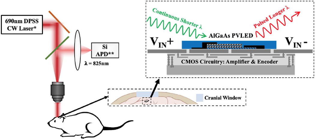
A simplified schematic of MOTEs-based neural recording [12], [14]. *DPSS CW Laser: Diode-Pumped Solid-State Continuous Wavelength Laser. **Si APD: Silicon Avalanche Photodiode.
Fig. 2 shows a system-level block diagram for the MOTE circuitry [12], [14], and Fig. 3 illustrates an example of a MOTE operation – 500Hz, 500μVPP test signal is applied at the input differential electrodes, amplified and encoded into optical pulses, and finally detected by a photodetector (PD). The detected pulses’ timing, namely their spacing (Δt), can then be used to recover the original sinusoid input.
Fig. 2.

Fig. 3.

A MOTE decoding example [12].
While the MOTE’s two main pillars, PVLED and the CMOS have individually been studied in detail [12], [14], [18], discussion of the associated integration challenges has been lacking. Given the MOTE’s size scale, wire-bonding is out of the question for interconnecting PVLED and MOS: a single wire-bond-pad footprint is larger than the MOTE. Furthermore, such bendable wire-bonds jeopardize the insulation needed for chronic recording inside a biological medium. We have instead photolithographically integrated the PVLED and the CMOS to result in a scalable and robust system. We have optimized the polymer-based transfer method [18], [19] and dielectric cladding to allow MOTEs to survive in a mouse brain for two months (and counting). We also discuss a practical insertion method that has been lacking – a μ-pipette approach to allow users to manipulate and insert the MOTEs with a minimal learning curve.
III. Results
A. PVLED Transfer on CMOS
The following integration process is based on a 180nm foundry CMOS process, whose top metal is aluminum. A MOTE has four contact points: VIN+, VIN−, VDD, and VSS. The VDD and VSS are to be connected to the PVLED (i.e. anode and cathode) while the two input electrodes are to be coated with platinum for biocompatibility. Although it is crucial to have a planar surface for a successful PVLED transfer and its adhesion to the CMOS, a CMOS die is not chemical-mechanically polished (CMP) after its final dielectric deposition (i.e. the dielectric on top of the top metal) – instead, there is 1~2μm of relief in the SixOyNz dielectric on top of the top metal layer. Hence, we start the integration fabrication with CF4 reactive ion etch (RIE) on the CMOS (Oxford 80: 150 W, 40 mTorr, 30 sccm CF4) for about 30 minutes in total. This etch removes all the dielectric above the top metal while the aluminum acts as an etch stop (high selectivity against the CF4 etch). It should be noted that ‘pad opening’ designation (the foundry selectively removes dielectric on top of the top metal for bondpads) is not used as the pad opening designation incurs 100~200nm of unremovable (by the CF4 etch) residues at the opening boundaries (suspected to originate from techniques used to make the openings at the foundry), detrimental to the subsequent PVLED transfer.
Following the dielectric removal, we transfer an AlGaAs μLEDs array that have been tailored to match the CMOS layout, using poly (methyl methacrylate) (PMMA) transfer techniques often used in 2D materials transfers [18, 19]. while both the VDD and the VSS aluminum pads are directly below the cathodic layer of the PVLED, they do not form ohmic contacts alleviating leakage concerns.
B. CMOS Integration
The transfer results in PVLED on CMOS with the PMMA still intact. To cleanly remove the PMMA, we employ a high vacuum annealing (Custom-built: 320°C for 2 hours at less than 10−6 Torr, 30-minute ramp from room temperature, and natural cool-down). This anneal not only removes the PMMA better than oxygen plasma it also enhances the adhesion between the CMOS and the μLEDs (simply using solvent to remove PMMA also washes the μLEDs off the CMOS surface). Post annealing, it is possible to rinse with solvent as well as deionized water (DI) to better remove polar residues for more than 15 minutes, further reducing the transfer process residues. Fig. 4 compares the before and the after the anneal. Importantly, any excess residues will later inhibit the cladding layer deposition and cause biological media to leak in.
Fig. 4.
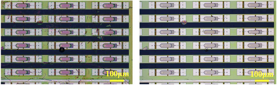
AlGaAs μLEDs transferred on top of the MOTE CMOS die, before annealing (left) and after annealing (right).
After the annealing and the residue cleaning, ~90nm SiO2 is deposited using atomic layer deposition (ALD) (Oxford FlexAL: 200°C, Plasma enhanced) to fill micro-cracks and voids, and further the adhesion of the PVLEDs on CMOS. We have found that a temperature lower than 200 °C results in SiO2 with inadequate quality for cladding. Fig. 5 illustrates the ensuing fabrication steps based on four-mask contact lithography.
Fig. 5.

MOTEs integration fabrication flow.
1). Contact:
AZ® nLOF 2002 resist is used with ABM contact aligner to define contact openings. CHF3/O2 reactive ion etch (RIE) (Oxford 80: 200 W, 50 mTorr, 50 sccm CHF3, 2 sccm O2, 9 minutes) removes the ALD SiO2 in the openings. Then buffered oxide etch (BOE, 6:1, 60 seconds) is used to remove naturally forming aluminum oxide, and form undercuts beneath the nLOF resist. Shortly after the BOE etch, the MOTE is placed inside a sputter for RF sputtering [20] (AJA: Base Pressure < 10−6 Torr, RF = 50W, Ti ~ 5nm for adhesion, Pt ~ 50nm at 20mTorr), and lifted off in Shipley MICROPOSIT® REMOVER 1165.
2). Routing:
AZ® nLOF 2002 resist is used again with the ABM contact aligner as in 1) contact openings. Because there is no undercut this time, DC sputtering is used (AJA: Base Pressure <10−6 Torr, Ti ~ 10nm for adhesion, Pt ~ 90nm at 20mTorr) and it is lifted off in the 1165 as before. There is a trade-off between the thickness of Pt (lower resistance) and the film stress & lift-off viability – we have found that ~100nm to be an optimal point. Also, because the routing metal has to cover uneven topologies, electron beam (e-beam) evaporation is not suitable for this step. Following the routing, ~10nm ALD Si3N4 (Oxford FlexAL: 350°C, Plasma enhanced) and ~90nm ALD SiO2 (Oxford FlexAL: 200°C, Plasma enhanced) are deposited to insulate the routing metals. We find that the performance of MOTEs typically improves post the ALD deposition, likely owing to the thermal annealing effect during the step.
3). Top Etch:
This step separates each MOTE in the array. Because we must etch through inter-metal dielectric (IMD) and into the bulk silicon, we use Cr hard mask to withstand the required prolonged etch. RF sputtering is used to deposit the Cr (AJA: Base Pressure <10−6 Torr, RF = 50W, Cr ~ 100nm at 30mTorr). MEGAPOSIT™SPR™220-3.0 resist is used with the ABM contact aligner, and the Cr is selectively etched away using TRANSENE CHROMIUM ETCHANT 1020AC. After the Cr etch, the remaining resist is not stripped to serve as an additional etch mask to the Cr.
Inductively coupled plasma (ICP) RIE plasma etch is then used to etch the IMD (Oxford PlasmaPro 100 RIE: ICP = 3000W, RF = 60W, 4mTorr, 20sccm CH2F2, 80sccm He). While the ICP RIE provides excellent etch rate and vertical etch profile, it is difficult to guarantee sufficient thermal cooling because the tool is made for four-inch wafers and larger, whereas CMOS die are typically on the order of millimeters. Therefore, we have employed a Si carrier wafer that is as thin as possible without being too fragile (four-inch, 400μm thick, double side polish (DSP) wafer) and attached our die using AI Technology, Inc. COOL-GREASE™(CGR7016). We have also programmed the etcher to cycle the etch (30s etch followed by 60s cooling). Even with the high power of the ICP RIE, ~ 1hr of etching time is required to remove the IMD, which is ~10μm of SiXOYNZ.
We have noticed that the IMD color differs depending on whether the underlying bulk silicon is defined as diffusion layer or not during the tapeout. Hence, we have defined a section of the etch area to contain both the diffusion and nondiffusion area, so that it is optically apparent when the IMD is all etched away, and Si is exposed.
Following the IMD etch, we used deep-RIE (DRIE) (Unaxis 770 Deep Silicon Etcher) to etch away ~25μm of the bulk silicon. Together with the IMD thickness (~10μm), this defines the maximum thickness of MOTEs. This is because subsequent fabrication steps include thinning the backside silicon until the ~25μm deep trenches appear.
4). Cladding and Opening:
Following 3) Top Etch, both the remaining resist and the Cr are removed by oxygen plasma and the Cr Etch, respectively. Then, plasma enhanced chemical vapor deposition (PECVD) (OxFORD PlasmaPro 100 PECVD) is used to deposit ~200nm low stress SiXNY (139MPa, Tensile) followed by ~900nm tetraethyl orthosilicate (TEOS) SiO2. Furthermore, ~50nm ALD Al2O3 (Oxford FlexAL: 200°C, Plasma enhanced) is additionally deposited. While this cladding is needed to ensure longevity of the MOTEs inside biological media, input electrodes must be exposed. The photolithographic step is similar to the one shown in c) Top Etch – SPR330-2.0 atop sputtered Cr.
For the opening etch, the 3000W ICP RIE cannot be used as the extreme plasma density seems to damage the input capacitor in the CMOS circuitry. Therefore, we resorted to a lower power ICP RIE and a regular RIE which, while slower, are less damaging. We first etched away the Al2 O3 using BCl3/Ar ICP RIE (PlasmaTherm 770: ICP = 800W, RF = 15W, 7mTorr, 45sccm BCl3, 5sccm Ar), followed by CHF3/O2 RIE etch (Oxford 80: 240W, 40mTorr, 50sccm CHF3, 2sccm O2) to remove the remaining dielectric. The same etching is then repeated on the backside of the MOTEs chip as the conformal nature of the ALD and PECVD often leads to the unwanted dielectric deposition on the backside. Then the SPR220 photoresist and Cr are removed as in 3) Top Etch.
5). Backside Thinning:
The final step, thinning, is done through DRIE (Unaxis 770 Deep Silicon Etcher), which while being efficient in terms of the etch rate, suffers from the same issues as the ICP RIE during IMD etch – heating and handling. While Cornell NanoScale Facility (CNF) possesses higher power (hence faster etch) DRIE (PlasmaTherm Deep Silicon Etcher: 3000W vs. 800W of the Unaxis), we opted for the lower power Unaxis due to heating concerns. Therefore, we first spun the SPR 330-2.0 resist on a 400μm thick DSP wafer, and before the resist bake, the MOTEs die is placed upside down against the freshly spun resist, and gently pressed before being baked for twice the typical soft-bake time. Lastly, DRIE (Unaxis 770 Deep Silicon Etcher) is used in cycles, 40 loops at a time (follow by 30 seconds of cooling on a room temperature chill plate) to minimize the excess heating, until the trenches defined in the c) Top Etch appear.
It is important to note that if there are any residues present in between the CMOS and the μLEDs, then the heating is exacerbated and the MOTEs can be destroyed during this DRIE or ICP RIE etching for 3) Top Etch, as the authors found, painfully, prior to the adaptation of the high vacuum annealing.
Once the trenches appear, we immerse the MOTEs on the carrier wafer in acetone, and through medium exchange, the MOTEs are transferred to isopropanol, and finally to sterile water. Fig. 6 shows a fully released MOTE post the integration fabrication.
Fig. 6.

A scanning electron microscope (SEM) image of a fully released MOTE.
Table 1 describes the yield of the integration fabrication from the latest run. As shown, the μLEDs transfer is often perfect (the transfer yield rarely drops below 90%), and most failures are likely incurred during the integration fabrication. Though μLEDs may get damaged (i.e. micro cracks) during the transfer, this is hard to ascertain at the time of transfer.
TABLE I.
A Yield Table of Motes Fabrication
| MOTE_V5_C24 | 1 | 2 | 3 | 4 | 5 | 6 | 7 | 8 | 9 |
|---|---|---|---|---|---|---|---|---|---|
| 1 | |||||||||
| 2 | |||||||||
| 3 | |||||||||
| 4 | |||||||||
| 5 | |||||||||
| 6 | |||||||||
| 7 | |||||||||
| 8 | |||||||||
| 9 | |||||||||
| 10 | |||||||||
| CMOS Platform | 90 | Dead Devices | 14.00 | ||||||
| uLED Trasnferred on | 90 | Alive Devices | 76.00 | ||||||
| Transfer Yield (%) | 100 | Total Yield (%) | 84.44 | ||||||
An interesting phenomenon we have noticed is that once the MOTEs are released, and in a solution (i.e. saline), if there are any cracks in the encapsulation, inorganic ‘black mold’ quickly appears upon exposure to light. We speculate that this is likely due to an unwanted electrochemical interactions powered by the PVLED. Micro-bubbles near the cracks can also be observed during such failure processes – typically the micro-bubble sites quickly turn into ‘black mold’ sites. Fig. 7 compares a successful MOTE against its defective counterpart.
Fig. 7.
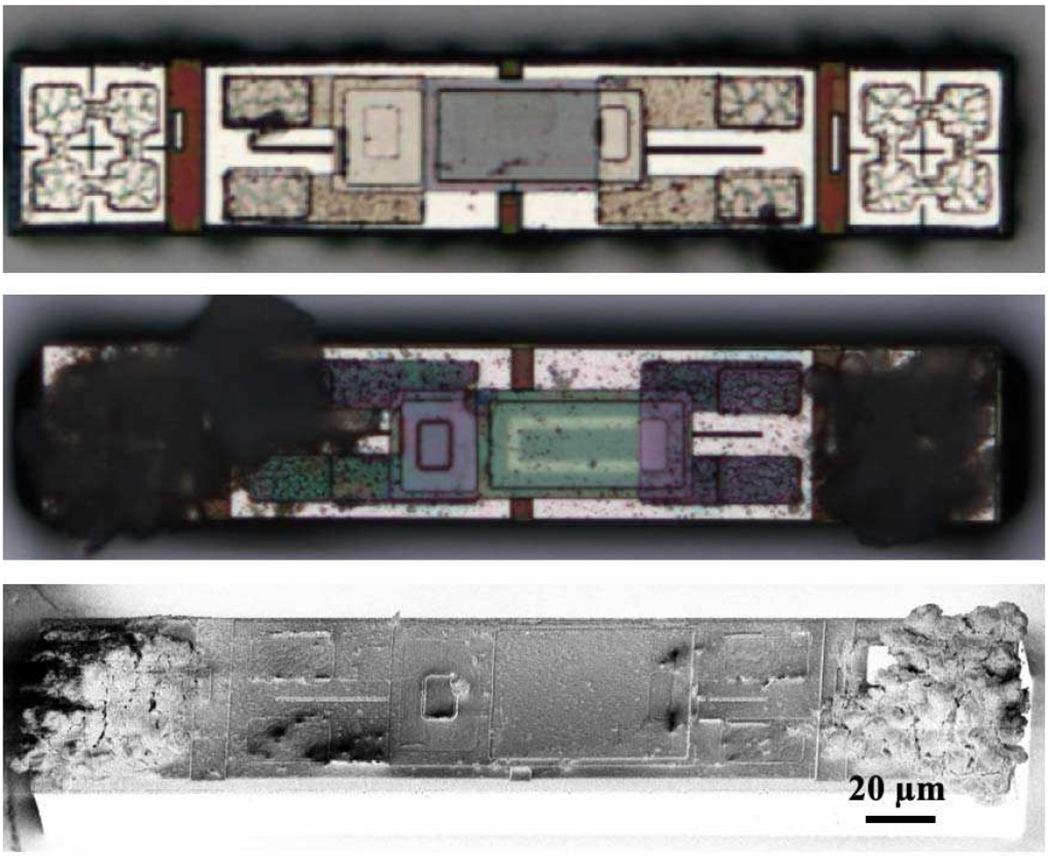
Successful encapsulation (top) vs. defective encapsulation (middle). The bottom is a SEM image of the middle.
IV. Handling and Insertion
Once the MOTEs are in a sterile solution, individual MOTEs are nearly invisible to a naked eye, making them extremely difficult to handle. We have found using μ-pipettes (with fiber) under a stereoscope (Thermo Fisher Scientific Fisher Stereomaster F1411-D830-002) to be the most straightforward method to handle and insert MOTEs. Once a μ-pipette is inserted near a MOTE in solution, capillary forces draw solution into the pipette, along with a MOTE. The μ-pipette tip can then be placed in contact with a paper wipe (we have used Kimberly-Clark Kimtech Science Kimwipes), and as the wipe absorbs solution inside the μ-pipette, the MOTE will be brought to the tip of the pipette. Thanks to the light weight of the MOTE (~1μg), the van der Waals attraction between the μ-pipette and the MOTE is enough to keep the MOTE intact inside the now-dry μ-pipette while moving.
To insert the MOTE into the brain, we have affixed the MOTE-containing μ-pipette to a X-Y-Z micro-positioner and inserted a stainless-steel wire into the μ-pipette as a push mechanism. Once the cranial opening is made, the μ-pipette is brought to touch down on dura. Because a MOTE is similar to a razorblade in its dimensions, it is possible to puncture the dura with the MOTE (i.e. the μ-pipette, which is bigger than the MOTE, stays outside dura, minimizing the insertion damage). Fig. 8 depicts the insertion scheme and a in vivo insertion into a mouse brain.
Fig. 8.

A MOTE insertion using a pulled μ-pipette. The left shows a simplified insertion mechanism while the right shows an in vivo insertion.
Each MOTE insertion can take as little as five minutes after a few practice sessions, and we have routinely implanted four to eight MOTEs each surgery. Once the MOTEs are inserted, a head bar window is installed to allowed for awake neural recording. Fig. 9 shows a mouse with the head bar and a typical in vivo measurement setup. While we have yet to obtain a neural signal from the MOTE (as inserting MOTEs near active neurons is largely chance based), Fig. 10 demonstrates that the inserted MOTEs are functioning properly, outputting pulses (insertion depth ~200μm, optical power ~23mW/mm2).
Fig. 9.

A mouse with a head bar window, ~2 months after the insertion surgery (left). The right shows the mouse (awake) under measurement using a head-bar fix apparatus.
Fig. 10.

A MOTE measurement in vivo. While the decoded signal (bottom) did not show a neural response, the observed optical pulses (top) indicate that the MoTE is functioning as designed.
V. Conclusion
For chronic, tetherless neural recording, MOTEs provide a compelling alternative to existing modalities such as electrodes shanks and coils/ultrasound-based implants. The heterogenous integration described in this manuscript has not only enabled the MOTE to be scaled down below human hair width, but also enabled the MOTEs to be fabricated en masse with high yield, proving scalability of the technology. Table II compares the MOTEs against state-of-the-arts.
TABLE II.
Table of Comparison
| Integrated Neural Interface [6] | Microwave Backscattering [21] | Neural Dust [11] | MOTE [This Work] | |
|---|---|---|---|---|
| Wireless Power Source | RF Coil | RF | Ultrasonic | Optical |
| Technology (nm) | 500 | - | 65 | 180 |
| Gain (dB) | 60 | - | 24 | 24 |
| Bandwidth (KHz) | 5 | 5 | 5 | 10 |
| Noise Floor (μVRMS) | 5.1 | 63 | 5.3 | 15 |
| Power | 135μW | 0 | 37.7 | <1μW |
| Cross-sectional Diameter | >300μm | >10mm | >500μm | >57μm |
| Volume per Channel (mm3) | >10 | 360 | 0.8 | <1x10⁻³ |
| Functional Depth (mm) | Surface Only | Surface Only | 50 | <5 (est.) |
| Functional Depth/Volume per Channel (mm−2) | - | - | 61.7 | <5x10³ |
MOTEs can survive in biological media for months timescale, can easily be integrated with standard microscopy systems, and can be handled with μ-pipettes that many biologists are familiar with. Furthermore, the proposed fabrication and handling methodologies are applicable to other types of heterogeneously integrated CMOS systems.
Acknowledgment
The authors would like to thank Haining Wang, Sanghoon Chae, Jaebin Choi, and Changhyuk Lee for critical discussions.
This work was supported by the National Institutes of Health under awards numbers R21-EY027581 and U01-NS107687. This work was performed in part at the Cornell NanoScale Facility, a member of the National Nanotechnology Coordinated Infrastructure, which is supported by the National Science Foundation under Grant ECCS-1542081, and made use of the Cornell Center for Materials Research Facilities supported by the National Science Foundation under award number DMR-1120296.
Biographies
Sunwoo Lee (M’2010) received the B.S. degree in electrical and computer engineering from Cornell University, Ithaca, NY, USA, in 2010, and the M.S. and Ph.D. degrees in electrical engineering from the Columbia University, NY, USA, in 2012 and 2016, respectively, working graphene-based nanoelectro-mechanical systems for signal processing and sensing applications.
In April 2016 he joined the Molnar Group as a postdoctoral researcher in the School of Electrical and Computer Engineering, Cornell University, Ithaca, NY, USA, to work on opto-electrically transduced micro-scale neural interfaces.

Alejandro Javier Cortese received the B.S. degree in Physics with highest honors and the B.S. degree in Mathematics from Duke University, Durham, NC, USA in 2012, the M.S degree and the Ph.D. degree in Physics from Cornell University, Ithaca, NY, USA in 2015 and 2019, respectively. He is a Presidential Postdoctoral Fellow at Cornell University, Ithaca, NY, USA working on wireless optoelectronic sensors.

Aaron Mok is a Ph.D. candidate in Biomedical Engineering at Cornell University, under the supervision of Prof. Chris Xu. He is interested in the development of neurotechnology, with a focus on advancing optical tools to image and study neuroactivities. Prior to Cornell, Aaron Mok obtained degrees with MPhil in Electrical and Electronic Engineering under the supervision of Dr. Kevin Tsia, BBA in Marketing and BEng in Medical Engineering at The University of Hong Kong.

Chunyan Wu received the B.S. degree in Bioengineering and Biomedical Engineering from Hefei University of Technology in 2012, and M.Eng. in Biomedical Engineering from Cornell University in 2014. She is currently a Ph.D. candidate in Biomedical Engineering at Cornell University.

Tianyu Wang studied Applied Physics from Shanghai Jiao Tong University before he transferred and received his B.S. degree in Biological and Environmental Engineering from Cornell University, Ithaca, NY, USA. In 2012. He received his Ph.D. in Applied Engineering Physics from Cornell University in 2018, during which period he developed three-photon calcium imaging technology. He is currently a Mong senior Cornell Neurotech fellow, and a postdoctoral researcher working on optical computing in McMahon Lab at Cornell University.

Ju Uhn (Mike) Park is a senior majoring in computer science and minoring in Policy Analysis and Management at Cornell University, Ithaca, NY. He joined the Molar Group in June 2019 to develop a graphical user interface for microscale opto-electronically transduced electrodes (MOTEs) system.
Conrad Smart received the B.S. degree in Physics and Mathematics from University of Louisville, Louisville, KY, USA in 2017, and he is currently pursuing his Ph.D. in Physics at Cornell University, Ithaca, NY, USA.

Shahaboddin Ghajari (M’2018) received the B.S. degree from Ferdowsi University of Mashhad, Mashhad, Iran and M.S. degree from Sharif University of Technology, Tehran, Iran in Electrical Engineering in 2015 and 2017 respectively. He is currently pursuing his Ph.D. in Electrical and Computer Engineering with Molnar Group at Cornell University, Ithaca, NY, USA.

Devesh Khilwani received the B.Tech. and M.Tech. degree in electrical engineering from IIT Bombay, India in 2019. Currently, he is a graduate student with the Molnar Group in the School of Electrical and Computer Engineering at Cornell University, Ithaca, NY, USA, working on biosensors.

Sanaz Sadeghi (M’2019) received her B.Sc. and M.Sc. degrees in electrical engineering from Sharif University of Technology, Tehran, Iran, in 2015 and 2017, respectively. Currently, she is a Ph.D. student with Molnar Group in electrical and electronics engineering at Cornell University, Ithaca, NY, USA.

Yanxin Ji received his B.S. in Physics from Peking University, Beijing, China in 2014. He is currently a Ph.D. candidate in Physics at Cornell University, Ithaca, NY, USA, working on 2D materials sensors.

Jesse H. Goldberg received his B.S. from Haverford College and his M.D./Ph.D. degrees from Columbia University. His Ph.D. with Rafa Yuste focused on dendritic computation and microcircuits of the cerebral cortex. In medical school, he became interested disorders such as Parkinson’s and dystonia that impair basal ganglia dependent reinforcement learning. His postdoctoral work at MIT focused on how the basal ganglia implement RL in juvenile songbirds. His lab combines high channel count awake-behaving electrophysiology, closed-loop optogenetics, and machine learning-guided behavioral analysis to study how animals learn through practice. Jesse has been supported by the Pew, Klingenstein, Kavli, NIH New Innovator and Cornell Neurotech. His guiding philosophy is that comparative approaches (across species and across the animal-machine divide) are necessary to distinguish general principles from behavior-, effector-, machine- and species-specific solutions to motor learning problems.

Chris Xu is Professor of Applied and Engineering Physics, Cornell University, the Mong Family Foundation Director of Cornell Neurotech – Engineering, and the director of Cornell NeuroNex Hub, an NSF funded center for developing neurotechnology. Prior to Cornell, he was a member of technical staff at Bell Laboratories, where he developed new long haul fiber optic communication systems. He received his Ph.D. in Applied Physics from Cornell University, and his B.S. degree in Physics from Fudan University, Shanghai, China. His current research areas are biomedical imaging and fiber optics. He is a fellow of the Optical Society of America, and a fellow of the National Academy of Inventors.

Paul L. McEuen received the B.S. degree in engineering physics at the University of Oklahoma, Norman, OK, USA in 1985, and Ph.D. in applied physics at Yale University, New Haven, CT, in 1991.
From 1990 to 1991, he worked as a postdoctoral researcher at MIT, Cambridge, MA, USA, before joining the faculty of the University of California, Berkeley, CA, USA. He moved to Cornell University in 2001, where he is currently the Goldwin Smith Professor of Physics. He is a member of the National Academy of Sciences and American Physical Society Fellow.

Alyosha Christopher Molnar (M’2007-S’2018), received the B.S. degree in engineering with highest honors from Swarthmore College, Swarthmore, PA, USA, in 1997, and the M.S. and Ph.D. degrees in electrical engineering from the University of California, Berkeley, CA, USA, in 2003 and 2007, respectively. From 1998 to 2002, he was with the RF IC Group at Conexant Systems, Inc. (now Skyworks Solutions, Inc.), Newport Beach, CA, USA, where he developed their first-generation GSM direct conversion receiver. In August 2007 he joined the faculty of the School of Electrical and Computer Engineering, Cornell University, Ithaca, NY, USA.
Contributor Information
Sunwoo Lee, The Department of Electrical and Computer Engineering, Cornell University in Ithaca, 14853 USA.
Alejandro Cortese, Department of Physics, Cornell University in Ithaca, 14853 USA.
Aaron Mok, Department of Biomedical Engineering, Cornell University in Ithaca, 14853 USA.
Chunyan Wu, Department of Applied and Engineering Physics, Cornell University in Ithaca, 14853 USA.
Tianyu Wang, Department of Applied and Engineering Physics, Cornell University in Ithaca, 14853 USA.
Ju Uhn Park, Department of Computer Science, Cornell University in Ithaca, 14853 USA.
Conrad Smart, Department of Physics, Cornell University in Ithaca, 14853 USA.
Shahaboddin Ghajari, Department of Electrical and Computer Engineering, Cornell University in Ithaca, 14853 USA.
Devesh Khilwani, Department of Electrical and Computer Engineering, Cornell University in Ithaca, 14853 USA.
Sanaz Sadeghi, Department of Electrical and Computer Engineering, Cornell University in Ithaca, 14853 USA.
Yanxin Ji, Department of Physics, Cornell University in Ithaca, 14853 USA.
Jesse H. Goldberg, Department of Neurobiology and Behavior, Cornell University in Ithaca, 14853 USA
Chris Xu, Department of Applied and Engineering Physics, Cornell University in Ithaca, 14853 USA.
Paul L. McEuen, Department of Physics, Cornell University in Ithaca, 14853 USA
Alyosha C. Molnar, Department of Electrical and Computer Engineering, Cornell University in Ithaca, 14853 USA.
References
- [1].Alivisatos A, Chun M, Church G, Greenspan R, Roukes M and Yuste R, “The brain activity map project and the challenge of functional connectomics,” Neuron, vol. 74, no. 6, pp. 970–974, 2012. [DOI] [PMC free article] [PubMed] [Google Scholar]
- [2].Buzsáki G, Stark E, Berényi A, Khodagholy D, Kipke D, Yoon E and Wise KD, “Tools for Probing Local Circuits: High-Density Silicon Probes Combined with Optogenetics,” Neuron, vol. 86, no. 1, pp. 92–105, April 2015. [DOI] [PMC free article] [PubMed] [Google Scholar]
- [3].Bai Q, Wise K and Anderson D, “A high-yield microassembly structure for three-dimensional microelectrode arrays,” in IEEE Transactions on Biomedical Engineering, vol. 47, no. 3, pp. 281–289, March 2000. [DOI] [PubMed] [Google Scholar]
- [4].Michon F, Aarts A, Holzhammer T, Ruther P, Borghs G, McNaughton B and Kloosterman F, “Integration of silicon-based neural probes and micro-drive arrays for chronic recording of large populations of neurons in behaving animals,” Journal of Neural Engineering, vol. 13, no. 4, p. 046018, June 2016. [DOI] [PubMed] [Google Scholar]
- [5].Szarowski D, Andersen M, Retterer S, Spence A, Isaacson M, Craighead H, Turner J and Shain W, “Brain responses to micro-machined silicon devices,” Brain Research, vol. 983, no. 1-2, pp. 23–35, 2003. [DOI] [PubMed] [Google Scholar]
- [6].Harrison R, Watkins P, Kier R, Lovejoy R, Black D, Normann R and Solzbacher F, “A Low-Power Integrated Circuit for a Wireless 100-Electrode Neural Recording System,” in 2006 IEEE International Solid State Circuits Conference - Digest of Technical Papers, San Francisco, CA, pp. 2258–2267, 2006. [Google Scholar]
- [7].Jiang Z, Huxter JR, Bowyer SA, Blockeel AJ, Butler J, Imtiaz SA, Wafford KA, Phillips KG, Tricklebank MD, Marston HM and Rodriguez-Villegas E, “TaiNi: Maximizing research output whilst improving animals’ welfare in neurophysiology experiments,” Scientific Reports, vol. 7, no. 1, p. 8086, 2017. [DOI] [PMC free article] [PubMed] [Google Scholar]
- [8].Lee SB, Lee B, Kiani M, Mahmoudi B, Gross R and Ghovanloo M, “Fabrication and Microassembly of a mm-Sized Floating Probe for a Distributed Wireless Neural Interface,” in IEEE Sensors Journal, vol. 16, no. 2, pp. 475–484, 15 January 2016.27069422 [Google Scholar]
- [9].Seo D, Carmena JM, Rabaey JM, Alon E and Maharbiz MM, “Neural Dust: An Ultrasonic, Low Power Solution for Chronic Brain-Machine Interfaces,” arXiv:1307.2196, 2013. [Google Scholar]
- [10].Seo D, Neely RM, Shen K, Singhal U, Alon E, Rabaey JM, Carmena JM and Maharbiz MM, “Wireless Recording in the Peripheral Nervous System with Ultrasonic Neural Dust,” Neuron, vol. 91, no. 3, pp. 529–539, August 2016. [DOI] [PubMed] [Google Scholar]
- [11].Ghanbari MM, Piech DK, Shen K, Alamouti SF, Yalcin C, Johnson BC, Carmena JM, Maharbiz MM and Muller R, “A Sub-mm3 Ultrasonic Free-Floating Implant,” IEEE JOURNAL OF SOLID-STATE CIRCUITS, vol. 54, no. 11, pp. 3017–3030, 2019. [Google Scholar]
- [12].Lee S, Cortese AJ, Gandhi A, Agger ER, McEuen PL and Molnar AC, “A 250 μm × 57 μm Microscale Opto-electronically Transduced Electrodes (MOTEs) for Neural Recording,” IEEE transactions on biomedical circuits and systems, vol. 12, no. 6, pp. 1256–1266, 2018. [DOI] [PMC free article] [PubMed] [Google Scholar]
- [13].Podgorski K and Ranganathan G, “Brain heating induced by near-infrared lasers during multiphoton microscopy,” Journal of Neurophysiology, vol. 116, no. 3, pp. 1012–1023, 2016. [DOI] [PMC free article] [PubMed] [Google Scholar]
- [14].Lee S, Cortese AJ, Trexel P, Agger ER, McEuen PL and Molnar AC, “A 330μm×90μm opto-electronically integrated wireless system-on-chip for recording of neural activities,” in 2018 IEEE International Solid State Circuits Conference - Digest of Technical Papers, San Francisco, CA, pp. 292–294, 2018. [Google Scholar]
- [15].Hemmati H, Biswas A and Djordjevic IB, “Deep-Space Optical Communications: Future Perspectives and Applications,” Proceedings of the IEEE, vol. 99, no. 11, pp. 2020–2039, August 2011. [Google Scholar]
- [16].Haydaroglu I and Mutlu S, “Optical Power Delivery and Data Trans-mission in a Wireless and Batteryless Microsystem Using a Single Light Emitting Diode,” Journal of Microelectromechanical Systems, vol. 24, no. 1, pp. 155–165, February 2015. [Google Scholar]
- [17].Haydaroglu I, Ozgun MT and Mutlu S, “Optically Powered Optical Transmitter Using a Single Light-Emitting Diode,” in IEEE Transactions on Circuits and Systems I : Regular Papers, vol. 64, no. 8, pp. 2003–2012, 2017. [Google Scholar]
- [18].Cortese AJ, Smart CL, Wang T, Reynolds MF, Norris SL, Ji Y, Lee S, Mok A, Wu C, Xia F, Ellis NI, Molnar AC, Xu C and McEuen PL, “Microscopic Sensors using Optical Wireless Integrated Circuits,” Proceedings of the National Academy of Sciences of the United States of America, 2020. [DOI] [PMC free article] [PubMed] [Google Scholar]
- [19].Li X, Cai W, An J, Kim S, Nah J, Yang D, Piner R, Velamakanni A, Jung I, Tutuc E, Banerjee SK, Colombo L and Ruoff RS, “Large-Area Synthesis of High-Quality and Uniform Graphene Films on Copper Foils,” Science, vol. 324, no. 5932, pp. 1312–1314, 2009. [DOI] [PubMed] [Google Scholar]
- [20].Homma Y and Tsunekawa S, “Planar Deposition of Aluminum by RF/DC Sputtering with RF Bias,” ECS Journal of Solid State Science and Technology, vol. 132, no. 6, pp. 1466–1472, 1985. [Google Scholar]
- [21].Kiourti A, Lee C, Chae J and Volakis JL, “A Wireless Fully Passive Neural Recording Device for Unobtrusive Neuropotential Monitoring,” in IEEE Transactions on Biomedical Engineering, vol. 63, no. 1, pp. 131–137, January 2016. [DOI] [PubMed] [Google Scholar]