First-principles simulations are performed to shed light on moiré excitons in twisted MoS2/WS2 heterostructures.
Abstract
Moiré superlattices in van der Waals (vdW) heterostructures could trap long-lived interlayer excitons. These moiré excitons could form ordered quantum dot arrays, paving the way for unprecedented optoelectronic and quantum information applications. Here, we perform first-principles simulations to shed light on moiré excitons in twisted MoS2/WS2 heterostructures. We provide direct evidence of localized interlayer moiré excitons in vdW heterostructures. The interlayer and intralayer moiré potentials are mapped out based on spatial modulations of energy gaps. Nearly flat valence bands are observed in the heterostructures. The dependence of spatial localization and binding energy of the moiré excitons on the twist angle of the heterostructures is examined. We explore how vertical electric field can be tuned to control the position, polarity, emission energy, and hybridization strength of the moiré excitons. We predict that alternating electric fields could modulate the dipole moments of hybridized moiré excitons and suppress their diffusion in moiré lattices.
INTRODUCTION
Van der Waals (vdW) heterostructures formed by vertical stacks of two-dimensional (2D) crystals provide an unprecedented platform to engineer quantum materials with exotic physical properties [unconventional superconductivity (1, 2), fractal quantum Hall effect (3), and Bose-Einstein condensation (4)] and novel optoelectronic applications [quantum emitters (5, 6) and spintronic and excitonic devices (7–9)]. The most appealing route to engineer a vdW heterostructure is to introduce a lattice mismatch or a rotation misalignment between the 2D layers, resulting in a moiré superlattice with new length and energy scales to be explored for fascinating quantum phenomena (10–16). More recently, the formation and controlling of moiré excitons trapped by periodic moiré potentials have attracted substantial interest (17).
Following initial theoretical predictions (5, 13), a number of experimental observations of moiré excitons have been reported in vdW heterostructures of transition metal dichalcogenides (TMDs) (18–22). The 2D TMDs feature prominent excitonic effect owing to quantum confinement and reduced dielectric screening (23–25). Most TMD heterostructures host long-lived interlayer excitons with electron and hole separated at different layers due to type II band alignment (26, 27). When the periodicity of the moiré superlattice exceeds the Bohr radius of the moiré excitons, the excitons could become spatially localized and dispersionless in energy (12, 28). The localized moiré excitons are envisioned as programmable solid state analog of ultracold atoms in optical lattices (5, 18–20). In addition, their substantially reduced bandwidths render the moiré lattices an excellent platform for studying exotic quantum phases, from Hubbard model to Mott and Wigner crystals (29–31).
Despite the surge of experimental and theoretical research on moiré excitons in vdW heterostructures, first-principles perspectives on this subject remain conspicuously scarce, hampered by computational challenges. This is unfortunate because first-principles studies can provide critical insights and a level of atomistic details that are beyond the reach of experiments and phenomenological theories. In particular, first-principles modeling is an indispensable tool in exploring the large and ever-increasing family of vdW heterostructures. In this work, we attempt to fill the gap and carry out first-principles calculations to shed light on moiré excitons in twisted MoS2/WS2 heterostructures. Using a newly developed computational method, we provide direct evidence of localized interlayer moiré excitons in vdW heterostructures. We map out the inter- and intralayer moiré potentials based on spatial modulations of energy gaps. Nearly flat valence bands are observed in MoS2/WS2 heterostructures with small twist angles. We examine the dependence of localization and binding energy of the moiré excitons on twist angles of the heterostructures and predict that electric field can be tuned to control the position, polarity, emission energy, and hybridization strength of moiré excitons. Last, we propose that the formation of hybridized moiré excitons under alternating electric fields could suppress their diffusion in moiré lattices.
RESULTS
Moiré potential and local bandgap modulation
Figure 1 (A and B) shows the unit cells of two moiré superlattices, formed by twisting an MoS2/WS2 bilayer with angles θ = 3.48° and θ = 56.52°, respectively. The unit cells have the same lattice constant (5.25 nm) and number of atoms (1626). In both superlattices, there are three local motifs, labeled by A, B, and C, that preserve the threefold rotational symmetry (C3). The three motifs play a crucial role in determining the properties of the moiré lattices. The local stacking configurations around these high symmetry points are denoted by RX/Y and HX/Y, indicating that X atoms at the WS2 layer sit directly above Y atoms at the MoS2 layer. Note that the atomic structures of these motifs are different for the two superlattices.
Fig. 1. Moiré patterns in the MoS2/WS2 heterobilayer.
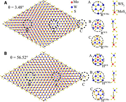
The unit cell of the moiré superlattice formed by a twisted MoS2/WS2 heterostructure with angle θ = 3.48° (A) and θ = 56.52° (B). The stacking configurations of the three local motifs, A, B, and C, are shown on the right.
A moiré superlattice can be considered as a collection of local stacking motifs—each characterized by a displacement vector d, defined in the primitive unit cell of the untwisted MoS2/WS2 bilayer (θ = 0°), shown in Fig. 2A. As d spans the primitive unit cell, all possible stacking motifs in MoS2/WS2 moiré superlattices can be recovered. In this way, one can map out the maximum amplitude of the moiré potentials, which is the most important property of the moiré superlattices. More specifically, we can calculate the energy bandgaps of the MoS2/WS2 bilayer (θ = 0°) as a function of d. The bandgap Eg is defined as the energy difference between the conduction band minimum (CBM) of MoS2 and the valence band maximum (VBM) of WS2. The bandgap variation δEg = Eg − 〈Eg〉 as a function of the stacking displacement d is shown in Fig. 2B, where 〈Eg〉 is the average bandgap. It is found that the bandgap extremes coincide with the high symmetry points of the moiré lattice. As the bandgap modulation is often used to characterize the moiré potentials (13), we reveal that the maximum value of the moiré potentials in MoS2/WS2 superlattices is ~100 meV at the A point, whereas the minimum value of the moiré potentials is −160 meV at the C point. The moiré potential at the B point is slightly shallower than that at the C point, and the maximum amplitude of the moiré potentials is thus ~260 meV. Note that the amplitude of a specific MoS2/WS2 bilayer could be lower than the maximum value of 260 meV.
Fig. 2. Moiré-modulated local energy gaps and interlayer distances.
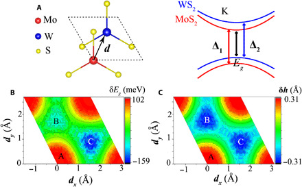
(A) The definition of in-plane displacement d in the primitive unit cell of the MoS2/WS2 heterostructure with θ = 0° (left). The definition of three bandgaps, Eg, Δ1, and Δ2 (right). (B) Variation of the MoS2/WS2 bandgap (Eg) as a function of d, showing three extremes at the A, B, and C points. (C) Variation of the interlayer distance δh as a function of d, with the extremes at the A, B, and C points.
Similarly, we can also estimate the maximum amplitudes of the intralayer moiré potentials by calculating the intralayer bandgap modulations, Δ1 and Δ2, defined in Fig. 2A. It is found that the maximum amplitudes of the intralayer moiré potentials are 18 meV for MoS2 and 13 meV for WS2, respectively (fig. S1). As the amplitude of the interlayer moiré potentials is much greater than that of the intralayer moiré potentials, the interlayer moiré excitons are expected to be more localized than the intralayer moiré excitons.
In Fig. 2C, we present the variation of interlayer distance (δh) as a function of d for MoS2/WS2 superlattices. Here, δh = h − <h>, with h defined as the vertical distance between the adjacent Mo and W atoms and <h> is its average value. It is found that the maximum δh occurs at the A point and the minimum at the B and C points. It is evident that the modulation of Eg tracks that of h, with the maximum (minimum) interlayer distance corresponding to the maximum (minimum) bandgap.
Flat valence bands and localized moiré excitons
In Fig. 3A, we present the single-particle band structure of the twisted MoS2/WS2 heterostructure with θ = 56.52°. A nearly flat VBM band is observed with the bandwidth of 3 meV, and the CBM bandwidth is 25 meV. The VBM and CBM are located at the Γ and K points of the Brillouin zone, respectively. As comparison, the valence bandwidth of the untwisted MoS2/WS2 heterostructure (θ = 0°) is 1500 meV. The corresponding charge densities of the VBM and CBM are shown in Fig. 3B. The VBM charge density extends to both layers with the main contribution from the pz and dz2 orbitals, giving rise to substantial interlayer mixing. In contrast, the CBM charge density is completely confined to the MoS2 layer. Thus, the VBM is modulated by the interlayer moiré potential, while the CBM by the intralayer moiré potential. Because the interlayer moiré potential is much deeper than the intralayer potential, the VBM charge density is more localized and the energy band is less dispersive than the CBM. In addition, the in-plane charge densities of the VBM and CBM show that the hole (blue) is more localized than the electron (red). If the single-particle pictures were accurate (with negligible excitonic effect), then the hole and the electron would have been trapped only at the C and B points, respectively.
Fig. 3. Flat bands in twisted MoS2/WS2 heterostructures.
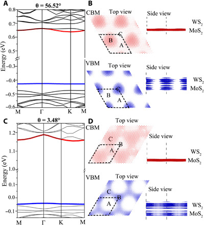
(A) The single-particle band structure for the MoS2/WS2 heterostructure with θ = 56.52°. The CBM and VBM bands are shown in red and blue, respectively. (B) Top and side views of the charge density of the CBM and VBM bands for the heterostructure. The unit cell of the moiré lattice is indicated by the dashed box. (C) Band structure for the MoS2/WS2 heterostructure with θ = 3.48°. (D) Top and side views of the charge density of the CBM and VBM bands for the heterostructure.
Similar results are also found in the MoS2/WS2 heterostructure with θ = 3.48°, shown in Fig. 3 (C and D). The VBM and CBM bandwidths are 7 and 34 meV, respectively. The hole is trapped at the B and C points but extends to both layers. In contrast, the electron is confined at the MoS2 layer, but delocalized within the layer. The flat valence bands in both heterostructures result from localized in-plane distributions of the holes. The formation of flat bands in the moiré superlattices is analogous to the formation of flat defect bands in semiconductors (28). The presence of moiré potentials introduces localized states at band edges, similar to localized defect levels in semiconductors; the periodicity of the moiré potential corresponds to the defect-defect distance. As the periodicity is increased, the defects become more isolated and their interactions diminish, leading to less dispersive defect bands. Evidently, “magic angles” are not required to form flat bands in TMD bilayers.
We have also examined the VBM bandwidths in MoS2/WS2 heterostructures with other twist angles, summarized in table S1. In general, as the twist angle increases from 0°, the VBM bandwidth increases. The band structures and charge densities of VBM and CBM for these heterostructures are shown in fig. S2. Last, we note that the CBM/VBM charge density distributions in the twisted MoS2/WS2 heterostructures are similar to those in the lattice-mismatched MoS2/MoSe2 heterostructure with no in-plane rotation (32).
The conventional first-principles approach to capture the excitonic effect in semiconductors is the GW-Bethe-Salpeter equation (GW-BSE) method (33–35) based on the many-body perturbation theory. However, the GW-BSE approach is prohibitively expensive for moiré excitons owing to the large number of atoms (~1600) in the unit cell. To circumvent the problem, we have recently developed an alternative first-principles method that can provide a reliable description of excitonic effect with much less computational cost (36–40). This method is based on time-dependent density functional theory (TDDFT) (41, 42), with optimally tuned and range-separated hybrid (RSH) exchange-correlation (XC) functionals (details are in Materials and Methods) (43–46). Using this method, we examine moiré excitons in twisted MoS2/WS2 heterostructures with different angles. In Fig. 4, we present the charge densities of excitons in the heterostructures with θ = 0°and θ = 3.48°. In the absence of a moiré potential (θ = 0°), the lowest-energy interlayer exciton is delocalized over the heterostructure, with the electron at the MoS2 and the hole at the WS2 layer. In the presence of the moiré potential (θ = 3.48 °), the low-energy moiré excitons become localized. In particular, the lowest-energy moiré exciton (E1 = 1.885 eV) is trapped at the C point, which has the lowest moiré potential. The hole distribution (blue) is more localized than the electron (red), consistent with the fact that the VBM is narrower than the CBM. The second lowest-energy moiré exciton (E2 = 1.901 eV) is trapped at the B point, again with the hole more localized than the electron. The third lowest-energy moiré exciton (E3 = 1.908 eV) has its electron trapped at the A point and the hole at the B and C points. The exciton charge density distributions (Fig. 4) deviate from the electron and hole distributions (Fig. 3) determined from the single-particle picture, which is a manifestation of the excitonic effect.
Fig. 4. Localized moiré excitons in the twisted MoS2/WS2 heterostructure (θ = 3.48°).
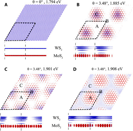
(A) Charge density and energy for the lowest-energy exciton in the MoS2/WS2 heterostructure with θ = 0° (upper panel, top view; bottom panel, side view). (B to D) Charge density and energy for the three lowest-energy moiré excitons in the twisted MoS2/WS2 heterostructure with θ = 3.48° (upper panel, top view; bottom panel, side view). The dashed box indicates the unit cell of the moiré superlattice. Red and blue colors represent the charge density of the electron and the hole, respectively. All iso-surface values are set at 0.0001 e/A3.
Localized moiré excitons are also observed in θ = 56.52° MoS2/WS2 heterostructure, shown in Fig. 5. The lowest-energy moiré exciton has its electron localized at the B point and hole at the C point, respectively. As the energy increases, the electron can also be localized at the A and C points, but the hole remains trapped at the C point primarily.
Fig. 5. Localized moiré excitons in the twisted MoS2/WS2 heterostructure (θ = 56.52°).
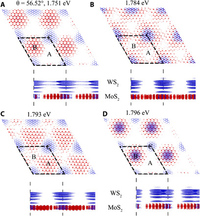
(A to D) Charge density and energy for the four lowest-energy moiré excitons in the twisted MoS2/WS2 heterostructure with θ = 56.52° (upper panel, top view; bottom panel, side view). The dashed box indicates the unit cell of the moiré superlattice. Red and blue colors represent the charge density of the electron and the hole, respectively. All iso-surface values are set at 0.0001 e/Å3.
As the twist angle increases, the moiré potential becomes shallower and the excitons become less localized (fig. S3). To the best of our knowledge, the present work provides the first direct evidence of localized moiré excitons in vdW heterostructures from first principles. Owing to the lateral confinement of moiré potentials, energy levels of the moiré excitons are quantized. For θ = 3.48°, the average energy spacing between the three lowest moiré excitons is merely 23 meV, compared with ~200 meV for θ = 0° (fig. S4). The small energy spacings imply that the spatial location of the moiré excitons may fluctuate at room temperature (KBT ~ 26 meV).
Last, we estimate exciton binding energy in various MoS2/WS2 heterostructures, summarized in table S1. Although the moiré excitons are localized in space, their binding energies are similar to that of delocalized interlayer exciton in the untwisted heterostructure. The binding energy of the interlayer excitons is determined primarily by the interlayer distance and the out-of-plane dielectric constant, both of which depend weakly on the twist angles. The similar weak dependence of the excitonic properties on local stacking motifs has also been observed from the GW-BSE calculations (47).
Electrical tuning of moiré exciton positions
The interlayer exciton features an electric dipole (P) that couples with a perpendicular electric field (ε), as shown schematically in Fig. 6A. This coupling enables electrical control of excitonic properties. On the one hand, the electric field could shift the energy levels of MoS2 and WS2 due to the Stark effect. A positive field, pointing from the WS2 to the MoS2 layer, would increase the energy of MoS2 and lower the energy of WS2, and vice versa for a negative electric field. The band structure changes due to the electric fields are shown in fig. S5 by considering spin-orbit coupling (SOC). Therefore, upon a certain positive field, the electron and hole of a moiré exciton could switch layers, forming an interlayer moiré exciton with the opposite polarity. On the other hand, the electric field can also switch the in-plane positions of the moiré excitons (5, 48). More specifically, because the A, B, and C points have different interlayer distance (h), as shown in Fig. 6B, they would have different coupling energy E according to E = eεh.
Fig. 6. Electric field tunable electronic structure in the MoS2/WS2 heterostructure.
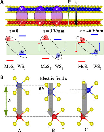
(A) Top: Schematic picture of the MoS2/WS2 heterostructure under a perpendicular electric field ε. The dipole moment of the interlayer exciton is indicated by P. Bottom: Electric tuning of the type II band alignment of the heterostructure. The red and blue arrows denote the energy level shift directions. (B) The variation of the interlayer distance h at the A, B, and C points for the MoS2/WS2 heterostructure with θ = 3.48°.
In the absence of electric field, the lowest-energy moiré exciton for θ = 3.48° is positioned at the C point, and the second lowest-energy moiré exciton at the B point, with an energy difference ∆E = 0.016 eV (see Fig. 4). Because ∆h = hC − hB = 0.05 Å, the exciton positions can be switched by a positive field . This is exactly what the first-principles calculations reveal. As shown in Fig. 7A, the lowest-energy moiré exciton shifts from C to B under a positive electric field of 3 V/nm. The electron and hole also switch layers, with the electron now residing at the WS2 layer and the hole at the MoS2 layer. In other words, the positive field can switch both position and polarity of the moiré excitons. Similarly, as hA − hC = 0.5 Å, one can apply a negative electric field to switch the exciton positions between A and C. Our first-principles calculations indicate that a field of −6 V/nm could shift the lowest-energy moiré exciton from C to A.
Fig. 7. Tuning moiré excitons in the twisted MoS2/WS2 heterostructure by electric field.
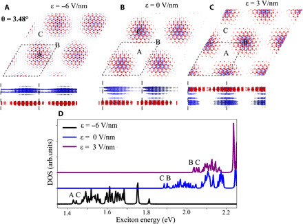
(A to C) The charge density distribution (top and side views) for the lowest-energy moiré exciton in the MoS2/WS2 heterostructure with θ = 3.48° under different electric fields. Red and blue colors represent the charge density of the electron and the hole, respectively. (D) The density of states (DOS) for the excitons under different electric fields, showing field-tunable exciton transition energies. The spatial locations (A, B, and C) for the two lowest-energy excitons are indicated.
As shown in Fig. 6A, a negative field can reduce the energy gap of the heterostructure, thus the energy of the interlayer excitons. In Fig. 7D, we present the density of excitonic states at three different electric fields. As the electric field varies from −6 to 3 V/nm, the exciton energy can be continuously tuned over a wide range of 600 meV, with red (blue) shift of the exciton energy under the negative (positive) field. To summarize, we have demonstrated that the electric field can be tuned to program the spatial location, polarity, and emission energy of moiré excitons, enabling control of quantum information carriers on demand.
Electrical tuning of exciton hybridization
As shown in Fig. 6A and fig. S5, under a positive electric field, the CBM and VBM of MoS2 are elevated, and the CBM and VBM of WS2 are lowered. These changes would promote resonant tunneling of the electron and hole across the heterojunction, leading to hybridized excitons (49, 50). In Fig. 8A, we present the charge density of the lowest-energy moiré exciton in θ = 56.5° heterostructure at ε = 0 and 3 V/nm. While there is a minor hybridization of the hole under zero electric field, the hybridization becomes much more prominent under ε = 3 V/nm. In the latter case, the electron (and hole) density spreads equally between the WS2 and MoS2 layers. In other words, the exciton can be considered as both intra- and interlayer exciton or, alternatively, a hybridized intra- and interlayer exciton.
Fig. 8. Tuning hybridized moiré excitons by electric field.
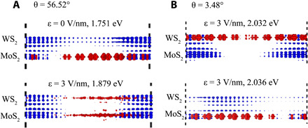
(A) The side view of the charge density distribution for the lowest-energy exciton in the MoS2/WS2 heterostructure with θ = 56.5° under different electric fields. Red and blue colors represent the charge density of the electron and the hole, respectively. (B) Side view of the charge density distribution for the two lowest-energy excitons in the MoS2/WS2 heterostructure with θ = 3.48° under the electric field of ε = 3 V/nm.
In Fig. 8B, we show the charge densities of the two lowest-energy moiré excitons in θ = 3.48° MoS2/WS2 heterostructure under an electric field ε = 3 V/nm. Although the two excitons have opposite polarity, they have almost the same energies (4 meV difference). Hence, they can be regarded as two approximately degenerate states, and their superposition would have the electron and hole spread evenly between the layers. In other words, hybridized moiré excitons can be formed in both heterostructures under the same field. Compared with the interlayer excitons whose dipoles are normal to the plane, the hybridized excitons could orient their dipoles in the plane. In addition, the dipole moment of the hybridized exciton could be reduced from that of the interlayer exciton.
Hybridized moiré excitons have been observed recently in MoSe2/WS2 heterostructures in which the degree of hybridization can be tuned continuously with the twist angle (21, 50, 51). Our calculations on the other hand show that the hybridization strength can also be tuned by electric field.
Diffusion of moiré excitons
Although the moiré excitons are localized, they can nonetheless tunnel through the moiré potentials and diffuse over long distances (52). Thus, the ability to control exciton diffusion—either enhancement or suppression—is of substantial interest. In a moiré superlattice, the diffusion of a moiré exciton can be modeled as a series of incoherent hops between the lattice sites with low moiré potentials. The Förster theory is often used to estimate the rates of energy transfer between two weakly coupled dipoles, i.e., moiré excitons at adjacent sites (53, 54). In the Förster theory, the relative orientation of the dipole moments can substantially influence the rates of energy transfer. This dependence is captured by the orientation factor κ defined as
Here, and are unit vectors defining the orientation of the dipole moments of the donor and the acceptor excitons, and is the unit vector connecting the two. In MoS2/WS2 heterostructures, always lies in the plane, connecting the high symmetry points (A, B, and C). As long as the interlayer moiré exciton is not hybridized, and are perpendicular to the plane, thus to , as shown schematically in Fig. 9A (left). In this case, the orientation factor κ is 1. When the exciton is hybridized, its dipole moment could lie in the plane, as shown in Fig. 9A (right). In this case, and would be perpendicular to , yielding κ = 0. The vanishing κ would suppress exciton diffusion, thus locking the exciton in space. Because the electric field can tune the degree of exciton hybridization, it could also modulate the κ value, thus controlling exciton diffusion. Thus, we predict that alternating electric fields could lead to oscillating dipoles of the moiré excitons, as shown in Fig. 9B, which suppress their diffusion.
Fig. 9. Tuning moiré exciton diffusion by electric field.
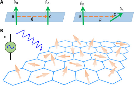
(A) Schematic diagram showing the dipole directions of a diffusing moiré exciton from the B point to the C point in a moiré superlattice. (B) Schematic picture depicting the fluctuation of the dipole moment of a diffusing moiré exciton under an alternating electric field.
Last, we provide a crude estimate for the diffusion of the lowest-energy moiré exciton in the MoS2/WS2 heterostructure with θ = 3.48°. The lifetime of the exciton is estimated on the basis of the spontaneous emission rate, and the exciton hopping rates are determined by the Förster theory (details in Materials and Methods). Using Monte Carlo (MC) simulations, we estimate that the lifetime of the moiré exciton is ~1 ns, similar to the experimental results of 1.8 ns in the MoSe2/WSe2 heterostructure (26) and 970 ± 180 ps in WS2/WSe2 heterostructures (52). Note that other experiments have reported much longer lifetimes (8, 55). On the other hand, localized moiré excitons are expected to have shorter diffusion lengths than the delocalized excitons in the untwisted heterostructure. We find that the diffusion length of the moiré exciton is 0.133 μm, one order of magnitude smaller than that in the WSe2/MoSe2 heterostructure (8). The diffusion constant of the moiré exciton is 0.2 cm2/s, which is in line with the experimental results (8).
DISCUSSION
The large family of 2D materials presents an unprecedented opportunity in engineering quantum materials. In particular, the presence of strongly bonded, long-lived, and localized interlayer moiré excitons in TMD heterostructures could open doors for applications, such as quantum emitters, high-performance lasers, twistronics (56), etc. Understanding, predicting, and ultimately controlling moiré excitons in vdW heterostructures are thus of great scientific importance, but yet highly challenging. In this work, we demonstrate that first-principles simulations are uniquely poised to address the challenges and offer critical insights that cannot be obtained otherwise. For example, first-principles simulations can provide atomic and electronic structures (e.g., bonding feature, charge density, band structure, atomic relaxation) that are not easily accessible to experiments. Although phenomenological theories and tight-binding models are commonly used in theoretical study of 2D materials, they often assume certain symmetries. When the symmetries are broken, such as the presence of inhomogeneous strains and lattice defects, they no longer can be used; first-principles simulations do not suffer these constraints.
In this work, we determine the spatial distributions of exciton charge densities in twisted MoS2/WS2 with first-principles calculations, providing the direct evidence of localized moiré excitons in TMD heterostructures. We map out the interlayer and intralayer moiré potentials that trap the moiré excitons. Both the magnitude and the periodicity of moiré potentials are found relevant to the formation of flat bands in TMD heterostructures, with the former responsible for the band position and the latter for the band dispersion. As the twist angle increases from 0°, the moiré superlattices shrink in sizes and the moiré excitons become less localized, but their binding energies remain essentially the same. We demonstrate that the vertical electric field can be tuned to control the position, polarity, emission energy, and hybridization strength of the moiré excitons. Although the required field can be quite large (~1 V/nm) in some cases owing to strong moiré potentials in MoS2/WS2, it could be lowered by various means, including using other TMD bilayers (e.g., MoSe2/WSe2) or twist angles with much weaker moiré potentials, using TMD trilayers, increasing the interlayer distance, and inserting a BN layer, etc. Last, we predict that alternating electric fields could lead to oscillating dipoles of the moiré excitons, thus suppressing their diffusion.
MATERIALS AND METHODS
First-principles ground-state calculations
The ground-state properties, including the single-particle band structure, ground-state charge density, and equilibrium geometry of MoS2/WS2 heterostructures are modeled by first-principles DFT, implemented in the Vienna Ab initio Simulation Package (57, 58). The Perdew-Burke-Ernzerhof XC functional (59) along with projector-augmented wave potentials (60, 61) are used in the self-consistent total energy calculations and geometric optimization. The vdW interaction is considered via the vdW-D2 exchange functional (62, 63). The energy cutoff for the plane-wave basis set is 400 eV. For the band structure calculations of θ = 3.48° and θ = 56.52° heterostructures, five special k-points are sampled along each of the high symmetry lines in the Brillouin zone. The atomic geometry in each moiré superlattice is fully optimized by relaxing all atoms until the residual force on each atom is less than 0.01 eV Å−1. A 20-Å vacuum layer is included in the calculations to separate the periodic images of the MoS2/WS2 slab. SOC is taken into consideration in the band structure calculations of the untwisted MoS2/WS2 heterostructure (θ = 0°) under different electric fields (fig. S5). The SOC splitting of the valence bands occurs only at the K point, and the splitting at the Γ point of VBM is zero. At the same time, the SOC splitting for CBM is negligible; thus, the bandgap remains indirect, independent of SOC. Thus, we believe that the presence of nearly flat VBM bands in the moiré superlattices with θ = 3.48° and θ = 56.52° will not be affected if the SOC was considered.
First-principles excited-state calculations
To determine the energies and the many-body wave functions of excitons in MoS2/WS2 heterostructures, we use a recently developed first-principles approach based on the linear-response TDDFT (LR-TDDFT) (41, 42), with an optimally tuned, screened, and range-separated hybrid XC functional (OT-SRSH) (43–46). The method has been implemented in conjunction with plane waves and pseudopotentials to study excitonic properties in semiconductors, including graphene fluoride, phosphorene, and 2D perovskites, and TMD heterostructures (36–40, 64).
The OT-SRSH involves the partition of the Coulombic interaction into a short-range and a long-range contribution based on the following expression (65)
| (1) |
The range-separated and hybrid XC functional can be expressed as
| (2) |
where is the Fock-like exact exchange energy, and and EKSc are the semilocal Kohn-Sham (KS) exchange and correlation energy, respectively. LR labels the long-range XC terms. α determines the contribution from the exact exchange, and β controls the contribution from the long-range exchange terms. γ is the range-separation parameter. In addition, α and β satisfy the requirement of α + β = ε0−1, where ε0 is the scalar dielectric constant of the solid, thereby enforcing the correct asymptotic screening of the Coulomb tail (44). The OT-SRSH functional can reproduce the correct long-range electron-electron and electron-hole interactions in solids by choosing the reasonable parameters. To reduce the computational cost associated with the Fock-like exchange on large systems, we apply first-order perturbation theory to the range-separated hybrid KS (RSH-KS) Hamiltonian and obtain the first order–corrected RSH-KS eigenvalues and eigenfunctions (36, 37). We then solve the following non-Hermitian eigenvalue equations of Casida (66)
| (3) |
where the pseudo-eigenvalue ωI is the Ith exciton energy level. The matrix elements of A and B in the basis of the KS states (ijσ) are given by
| (4) |
| (5) |
Here, K is the coupling matrix where indices i and k indicate the occupied orbitals, and j and l represent the virtual KS orbitals. According to the assignment ansatz of Casida, the many-body wave function of an excited state I can be written as
| (6) |
where ; is the annihilation operator acting on the ith KS orbital with spin σ, and Φ0 is the ground-state many-body wave function taken to be the single Slater determinate of the occupied KS orbitals.
In the (TD)DFT-OT-SRSH method, there are three parameters, α, β, and γ, needed to be specified. α controls the short-range exact exchange, and β is chosen to satisfy the requirement α + β = 1/ε0. The scalar dielectric constant of MoS2/WS2 heterostructure ε0 is set to 1.0, which is the correct asymptotic limit for screening in 2D materials (67). The other two independent parameters α = 0.06 and γ = 0.03 are determined by reproducing the fundamental gap of MoS2/WS2 heterojunction obtained from the one-shot GW calculations. The exciton binding energy, which is the difference between the fundamental gap and the optical gap Eb = Eg − Eopt is 0.50 eV, in good agreement with previous experimental and theoretical results (68–70). Thanks to the large unit cells (1626 atoms) in our LR-TDDFT calculations of the moiré excitons, only the Γ point is sampled in the Brillouin zone. We do not consider SOC correction in the LR-TDDFT calculations for the following reasons: (i) The SOC effect is known to be small at the Γ point with zero Rashba splitting for parabolic bands (71). (ii) The SOC has a negligible effect on the exciton charge densities. (iii) TDDFT-OT-SRSH calculations with SOC for such a large system (1626 atoms) are beyond our computational capability.
Exciton lifetime and diffusion constant calculation
We model the exciton diffusion as random walks using MC simulations (72). For a moiré exciton I, one can generate an event table with M + 2 transition probabilities (M is the number of the nearest-neighbor moiré excitons): transition probabilities from the exciton I to M neighboring excitons, P1,2, ⋯, M = kIJ × ∆t, with J = 1,2, ⋯, M; annihilation probability, PM + 1 = kI0 × ∆t; and the probability to remain at the same state I, PM + 2 = 1 − (P1 + P2 + ⋯ + PM + 1). ∆t is the time step of the MC simulations, which is set to be 10 fs. Here, we use Förster resonance energy transfer (54, 73) to determine the exciton transition rate kIJ as
| (7) |
where μI and μJ are the transition dipole moments of the states I and J, respectively. κ is a geometric factor, depending on the relative orientation of the dipoles. R is the distance between the center of mass of the two excitons, and Δω is the energy difference between the two excitons. The exciton annihilation lifetime is estimated on the basis of the spontaneous emission rate as
| (8) |
where c is the vacuum speed of light and n is the refractive index, which takes a value of 1.5 for MoS2/WS2. With the event table, a diffusion trajectory of the moiré exciton I is obtained by executing MC moves until the exciton is annihilated. From each trajectory, one can determine the lifetime t (the number of MC moves multiplied by Δt) and the maximum distance d of exciton diffusion. Averaging over all trajectories with the same initial exciton position gives the exciton diffusion length, lifetime, and diffusivity by LD = 〈d〉, τ = 〈t〉, and , respectively, where the brackets indicate the average.
Supplementary Material
Acknowledgments
Funding: This work was supported by the NSF (DMR1828019) and the Army Research Office (W911NF-20-10305). Author contributions: G.L. designed the study, and H.G. carried out calculations with the assistance of X.Z. G.L. supervised the research and wrote the manuscript with H.G. All authors discussed the results. Competing interests: The authors declare that they have no competing interests. Data and materials availability: All data needed to evaluate the conclusions in the paper are present in the paper and/or the Supplementary Materials. Additional data related to this paper may be requested from the authors.
SUPPLEMENTARY MATERIALS
Supplementary material for this article is available at http://advances.sciencemag.org/cgi/content/full/6/42/eabc5638/DC1
REFERENCES AND NOTES
- 1.Cao Y., Fatemi V., Fang S., Watanabe K., Taniguchi T., Kaxiras E., Jarillo-Herrero P., Unconventional superconductivity in magic-angle graphene superlattices. Nature 556, 43–50 (2018). [DOI] [PubMed] [Google Scholar]
- 2.Yankowitz M., Chen S., Polshyn H., Zhang Y., Watanabe K., Taniguchi T., Graf D., Young A. F., Dean C. R., Tuning superconductivity in twisted bilayer graphene. Science 363, 1059–1064 (2019). [DOI] [PubMed] [Google Scholar]
- 3.Dean C. R., Wang L., Maher P., Forsythe C., Ghahari F., Gao Y., Katoch J., Ishigami M., Moon P., Koshino M., Hofstadter’s butterfly and the fractal quantum Hall effect in moiré superlattices. Nature 497, 598–602 (2013). [DOI] [PubMed] [Google Scholar]
- 4.Eisenstein J., MacDonald A. H., Bose–Einstein condensation of excitons in bilayer electron systems. Nature 432, 691–694 (2004). [DOI] [PubMed] [Google Scholar]
- 5.Yu H., Liu G.-B., Tang J., Xu X., Yao W., Moiré excitons: From programmable quantum emitter arrays to spin-orbit–coupled artificial lattices. Sci. Adv. 3, e1701696 (2017). [DOI] [PMC free article] [PubMed] [Google Scholar]
- 6.Kumar S., Kaczmarczyk A., Gerardot B. D., Strain-induced spatial and spectral isolation of quantum emitters in mono- and bilayer WSe2. Nano Lett. 15, 7567–7573 (2015). [DOI] [PMC free article] [PubMed] [Google Scholar]
- 7.Rivera P., Seyler K. L., Yu H., Schaibley J. R., Yan J., Mandrus D. G., Yao W., Xu X., Valley-polarized exciton dynamics in a 2D semiconductor heterostructure. Science 351, 688–691 (2016). [DOI] [PubMed] [Google Scholar]
- 8.Jauregui L. A., Joe A. Y., Pistunova K., Wild D. S., High A. A., Zhou Y., Scuri G., De Greve K., Sushko A., Yu C.-H., Electrical control of interlayer exciton dynamics in atomically thin heterostructures. Science 366, 870–875 (2019). [DOI] [PubMed] [Google Scholar]
- 9.Morpurgo A. F., Gate control of spin-valley coupling. Nat. Phys. 9, 532–533 (2013). [Google Scholar]
- 10.Cao Y., Fatemi V., Demir A., Fang S., Tomarken S. L., Luo J. Y., Sanchez-Yamagishi J. D., Watanabe K., Taniguchi T., Kaxiras E., Correlated insulator behaviour at half-filling in magic-angle graphene superlattices. Nature 556, 80–84 (2018). [DOI] [PubMed] [Google Scholar]
- 11.Morell E. S., Correa J., Vargas P., Pacheco M., Barticevic Z., Flat bands in slightly twisted bilayer graphene: Tight-binding calculations. Phys. Rev. B 82, 121407 (2010). [Google Scholar]
- 12.Naik M. H., Jain M., Ultraflatbands and shear solitons in moiré patterns of twisted bilayer transition metal dichalcogenides. Phys. Rev. Lett. 121, 266401 (2018). [DOI] [PubMed] [Google Scholar]
- 13.Wu F., Lovorn T., MacDonald A. H., Topological exciton bands in moiré heterojunctions. Phys. Rev. Lett. 118, 147401 (2017). [DOI] [PubMed] [Google Scholar]
- 14.Bistritzer R., MacDonald A. H., Moiré bands in twisted double-layer graphene. Proc. Natl. Acad. Sci. 108, 12233–12237 (2011). [DOI] [PMC free article] [PubMed] [Google Scholar]
- 15.Kim K., DaSilva A., Huang S., Fallahazad B., Larentis S., Taniguchi T., Watanabe K., LeRoy B. J., MacDonald A. H., Tutuc E., Tunable moiré bands and strong correlations in small-twist-angle bilayer graphene. Proc. Natl. Acad. Sci. 114, 3364–3369 (2017). [DOI] [PMC free article] [PubMed] [Google Scholar]
- 16.Song J. C., Samutpraphoot P., Levitov L. S., Topological Bloch bands in graphene superlattices. Proc. Natl. Acad. Sci. 112, 10879–10883 (2015). [DOI] [PMC free article] [PubMed] [Google Scholar]
- 17.Tartakovskii A., Excitons in 2D heterostructures. Nat. Rev. Phys. 2, 8–9 (2020). [Google Scholar]
- 18.Tran K., Moody G., Wu F., Lu X., Choi J., Kim K., Rai A., Sanchez D. A., Quan J., Singh A., Evidence for moiré excitons in van der Waals heterostructures. Nature 567, 71–75 (2019). [DOI] [PMC free article] [PubMed] [Google Scholar]
- 19.Seyler K. L., Rivera P., Yu H., Wilson N. P., Ray E. L., Mandrus D. G., Yan J., Yao W., Xu X., Signatures of moiré-trapped valley excitons in MoSe2/WSe2 heterobilayers. Nature 567, 66–70 (2019). [DOI] [PubMed] [Google Scholar]
- 20.Jin C., Regan E. C., Yan A., Utama M. I. B., Wang D., Zhao S., Qin Y., Yang S., Zheng Z., Shi S., Observation of moiré excitons in WSe2/WS2 heterostructure superlattices. Nature 567, 76–80 (2019). [DOI] [PubMed] [Google Scholar]
- 21.Alexeev E. M., Ruiz-Tijerina D. A., Danovich M., Hamer M. J., Terry D. J., Nayak P. K., Ahn S., Pak S., Lee J., Sohn J. I., Resonantly hybridized excitons in moiré superlattices in van der Waals heterostructures. Nature 567, 81–86 (2019). [DOI] [PubMed] [Google Scholar]
- 22.Zhang N., Surrente A., Baranowski M., Maude D. K., Gant P., Castellanos-Gomez A., Plochocka P., Moiré intralayer excitons in a MoSe2/MoS2 heterostructure. Nano Lett. 18, 7651–7657 (2018). [DOI] [PubMed] [Google Scholar]
- 23.Ugeda M. M., Bradley A. J., Shi S.-F., Felipe H., Zhang Y., Qiu D. Y., Ruan W., Mo S.-K., Hussain Z., Shen Z.-X., Giant bandgap renormalization and excitonic effects in a monolayer transition metal dichalcogenide semiconductor. Nat. Mater. 13, 1091–1095 (2014). [DOI] [PubMed] [Google Scholar]
- 24.Chernikov A., Berkelbach T. C., Hill H. M., Rigosi A., Li Y., Aslan O. B., Reichman D. R., Hybertsen M. S., Heinz T. F., Exciton binding energy and nonhydrogenic Rydberg series in monolayer WS2. Phys. Rev. Lett. 113, 076802 (2014). [DOI] [PubMed] [Google Scholar]
- 25.Kylänpää I., Komsa H.-P., Binding energies of exciton complexes in transition metal dichalcogenide monolayers and effect of dielectric environment. Phys. Rev. B 92, 205418 (2015). [Google Scholar]
- 26.Rivera P., Schaibley J. R., Jones A. M., Ross J. S., Wu S., Aivazian G., Klement P., Seyler K., Clark G., Ghimire N. J., Observation of long-lived interlayer excitons in monolayer MoSe2–WSe2 heterostructures. Nat. Commun. 6, 6242 (2015). [DOI] [PubMed] [Google Scholar]
- 27.Rivera P., Yu H., Seyler K. L., Wilson N. P., Yao W., Xu X., Interlayer valley excitons in heterobilayers of transition metal dichalcogenides. Nat. Nanotech. 13, 1004–1015 (2018). [DOI] [PubMed] [Google Scholar]
- 28.Zhao X.-J., Yang Y., Zhang D.-B., Wei S.-H., Formation of Bloch flat bands in polar twisted bilayers without magic angles. Phys. Rev. Lett. 124, 086401 (2020). [DOI] [PubMed] [Google Scholar]
- 29.Shimazaki Y., Schwartz I., Watanabe K., Taniguchi T., Kroner M., Imamoğlu A., Strongly correlated electrons and hybrid excitons in a moiré heterostructure. Nature, 1–6 (2020). [DOI] [PubMed] [Google Scholar]
- 30.Tang Y., Li L., Li T., Xu Y., Liu S., Barmak K., Watanabe K., Taniguchi T., MacDonald A. H., Shan J., Simulation of Hubbard model physics in WSe2/WS2 moiré superlattices. Nature 579, 353–358 (2020). [DOI] [PubMed] [Google Scholar]
- 31.Regan E. C., Wang D., Jin C., Utama M. I. B., Gao B., Wei X., Zhao S., Zhao W., Zhang Z., Yumigeta K., Mott and generalized Wigner crystal states in WSe2/WS2 moiré superlattices. Nature 579, 359–363 (2020). [DOI] [PubMed] [Google Scholar]
- 32.Kang J., Li J., Li S.-S., Xia J.-B., Wang L.-W., Electronic structural moiré pattern effects on MoS2/MoSe2 2D heterostructures. Nano Lett. 13, 5485–5490 (2013). [DOI] [PubMed] [Google Scholar]
- 33.Hedin L., New method for calculating the one-particle Green's function with application to the electron-gas problem. Phys. Rev. 139, A796–A823 (1965). [Google Scholar]
- 34.Hybertsen M. S., Louie S. G., Electron correlation in semiconductors and insulators: Band gaps and quasiparticle energies. Phys. Rev. B 34, 5390–5413 (1986). [DOI] [PubMed] [Google Scholar]
- 35.Rohlfing M., Louie S. G., Electron-hole excitations in semiconductors and insulators. Phys. Rev. Lett. 81, 2312–2315 (1998). [Google Scholar]
- 36.Zhang X., Li Z., Lu G., A non-self-consistent range-separated time-dependent density functional approach for large-scale simulations. J. Phys. Conden. Matt. 24, 205801 (2012). [DOI] [PubMed] [Google Scholar]
- 37.Huang L.-y., Zhang X., Zhang M., Lu G., Effect of point defects on optical properties of graphene fluoride: a first-principles study. J. Phys. Chem. C 121, 12855–12862 (2017). [Google Scholar]
- 38.Huang L.-y., Zhang X., Zhang M., Lu G., Optically inactive defects in monolayer and bilayer phosphorene: A first-principles study. Phys. Rev. Mater. 2, 054003 (2018). [Google Scholar]
- 39.Gao Y., Zhang M., Zhang X., Lu G., Decreasing exciton binding energy in two-dimensional halide perovskites by lead vacancies. J. Phys. Chem. Lett. 10, 3820–3827 (2019). [DOI] [PubMed] [Google Scholar]
- 40.Nan G., Zhang X., Lu G., Self-healing of photocurrent degradation in perovskite solar cells: The role of defect-trapped excitons. J. Phys. Chem. Lett. 10, 7774–7780 (2019). [DOI] [PubMed] [Google Scholar]
- 41.Gross E., Kohn W., Local density-functional theory of frequency-dependent linear response. Phys. Rev. Lett. 55, 2850–2852 (1985). [DOI] [PubMed] [Google Scholar]
- 42.M. A. Marques, N. T. Maitra, F. M. Nogueira, E. K. Gross, A. Rubio, Fundamentals of Time-Dependent Density Functional Theory (Springer Science & Business Media, 2012), vol. 837. [Google Scholar]
- 43.Refaely-Abramson S., Jain M., Sharifzadeh S., Neaton J. B., Kronik L., Solid-state optical absorption from optimally tuned time-dependent range-separated hybrid density functional theory. Phys. Rev. B 92, 081204 (2015). [Google Scholar]
- 44.Refaely-Abramson S., Sharifzadeh S., Jain M., Baer R., Neaton J. B., Kronik L., Gap renormalization of molecular crystals from density-functional theory. Phys. Rev. B 88, 081204 (2013). [Google Scholar]
- 45.Wing D., Haber J. B., Noff R., Barker B., Egger D. A., Ramasubramaniam A., Louie S. G., Neaton J. B., Kronik L., Comparing time-dependent density functional theory with many-body perturbation theory for semiconductors: Screened range-separated hybrids and the GW plus Bethe-Salpeter approach. Phys. Rev. Mater. 3, 064603 (2019). [Google Scholar]
- 46.Refaely-Abramson S., Sharifzadeh S., Govind N., Autschbach J., Neaton J. B., Baer R., Kronik L., Quasiparticle spectra from a nonempirical optimally tuned range-separated hybrid density functional. Phys. Rev. Lett. 109, 226405 (2012). [DOI] [PubMed] [Google Scholar]
- 47.Lu X., Li X., Yang L., Modulated interlayer exciton properties in a two-dimensional moiré crystal. Phys. Rev. B 100, 155416 (2019). [Google Scholar]
- 48.Ciarrocchi A., Unuchek D., Avsar A., Watanabe K., Taniguchi T., Kis A., Polarization switching and electrical control of interlayer excitons in two-dimensional van der Waals heterostructures. Nat. Photon. 13, 131–136 (2019). [DOI] [PMC free article] [PubMed] [Google Scholar]
- 49.Huang D., Kaxiras E., Electric field tuning of band offsets in transition metal dichalcogenides. Phys. Rev. B 94, 241303 (2016). [Google Scholar]
- 50.Hsu W.-T., Lin B.-H., Lu L.-S., Lee M.-H., Chu M.-W., Li L.-J., Yao W., Chang W.-H., Shih C.-K., Tailoring excitonic states of van der Waals bilayers through stacking configuration, band alignment, and valley spin. Sci. Adv. 5, eaax7407 (2019). [DOI] [PMC free article] [PubMed] [Google Scholar]
- 51.Ruiz-Tijerina D. A., Fal'ko V. I., Interlayer hybridization and moiré superlattice minibands for electrons and excitons in heterobilayers of transition-metal dichalcogenides. Phys. Rev. B 99, 125424 (2019). [Google Scholar]
- 52.Yuan L., Zheng B., Kunstmann J., Brumme T., Kuc A. B., Ma C., Deng S., Blach D., Pan A., Huang L., Twist-angle-dependent interlayer exciton diffusion in WS2–WSe2 heterobilayers. Nat. Mater., 1–7 (2020). [DOI] [PubMed] [Google Scholar]
- 53.Şener M., Strümpfer J., Hsin J., Chandler D., Scheuring S., Hunter C. N., Schulten K., Förster energy transfer theory as reflected in the structures of photosynthetic light-harvesting systems. Chem. Phys. Chem. 12, 518–531 (2011). [DOI] [PMC free article] [PubMed] [Google Scholar]
- 54.Hennebicq E., Pourtois G., Scholes G. D., Herz L. M., Russell D. M., Silva C., Setayesh S., Grimsdale A. C., Müllen K., Brédas J.-L., Exciton migration in rigid-rod conjugated polymers: An improved Förster model. J. Am. Chem. Soc. 127, 4744–4762 (2005). [DOI] [PubMed] [Google Scholar]
- 55.Wang J., Ardelean J., Bai Y., Steinhoff A., Florian M., Jahnke F., Xu X., Kira M., Hone J., Zhu X.-Y., Optical generation of high carrier densities in 2D semiconductor heterobilayers. Sci. Adv. 5, eaax0145 (2019). [DOI] [PMC free article] [PubMed] [Google Scholar]
- 56.Carr S., Massatt D., Fang S., Cazeaux P., Luskin M., Kaxiras E., Twistronics: Manipulating the electronic properties of two-dimensional layered structures through their twist angle. Phys. Rev. B 95, 075420 (2017). [Google Scholar]
- 57.Kresse G., Efficient iterative schemes for ab initio total-energy calculations using a plane-wave basis set. Phys. Rev. B 54, 11169–11186 (1996). [DOI] [PubMed] [Google Scholar]
- 58.Kresse G., Furthmüller J., Efficiency of ab-initio total energy calculations for metals and semiconductors using a plane-wave basis set. Comput. Mater. Sci. 6, 15–50 (1996). [DOI] [PubMed] [Google Scholar]
- 59.Perdew J. P., Burke K., Ernzerhof M., Generalized gradient approximation made simple. Phys. Rev. Lett. 77, 3865–3868 (1996). [DOI] [PubMed] [Google Scholar]
- 60.Blöchl P., Projector augmented-wave method. Phys. Rev. B 50, 17953–17979 (1994). [DOI] [PubMed] [Google Scholar]
- 61.Kresse G., From ultrasoft pseudopotentials to the projector augmented-wave method. Phys. Rev. B 59, 1758–1775 (1999). [Google Scholar]
- 62.Grimme S., Semiempirical GGA-type density functional constructed with a long-range dispersion correction. J. Comput. Chem. 27, 1787–1799 (2006). [DOI] [PubMed] [Google Scholar]
- 63.Bucko T., Hafner J. R., Lebegue S., Angyán J. G., Improved description of the structure of molecular and layered crystals: Ab initio DFT calculations with van der Waals corrections. J. Phys. Chem. A 114, 11814–11824 (2010). [DOI] [PubMed] [Google Scholar]
- 64.Liu J., Zhang X., Lu G., Excitonic effect drives ultrafast dynamics in van der waals heterostructures. Nano Lett. 20, 4631–4637 (2020). [DOI] [PubMed] [Google Scholar]
- 65.Yanai T., Tew D. P., Handy N. C., A new hybrid exchange–correlation functional using the Coulomb-attenuating method (CAM-B3LYP). Chem. Phys. Lett. 393, 51–57 (2004). [Google Scholar]
- 66.D. P. Chong, Recent Advances in Density Functional Methods (World Scientific, 1995), vol. 1. [Google Scholar]
- 67.Andersen K., Latini S., Thygesen K. S., Dielectric genome of van der Waals heterostructures. Nano Lett. 15, 4616–4621 (2015). [DOI] [PubMed] [Google Scholar]
- 68.Torun E., Miranda H. P., Molina-Sánchez A., Wirtz L., Interlayer and intralayer excitons in MoS2/WS2 and MoSe2/WSe2 heterobilayers. Phys. Rev. B 97, 245427 (2018). [Google Scholar]
- 69.Kunstmann J., Mooshammer F., Nagler P., Chaves A., Stein F., Paradiso N., Plechinger G., Strunk C., Schüller C., Seifert G., Reichman D. R., Kohn W., Momentum-space indirect interlayer excitons in transition-metal dichalcogenide van der Waals heterostructures. Nat. Phys. 14, 801–805 (2018). [Google Scholar]
- 70.Chen H., Wen X., Zhang J., Wu T., Gong Y., Zhang X., Yuan J., Yi C., Lou J., Ajayan P. M., Ultrafast formation of interlayer hot excitons in atomically thin MoS2/WS2 heterostructures. Nat. Commun. 7, 1–8 (2016). [DOI] [PMC free article] [PubMed] [Google Scholar]
- 71.Mosconi E., Etienne T., De Angelis F., Rashba band splitting in organohalide lead perovskites: bulk and surface effects. J. Phys. Chem. Lett. 8, 2247–2252 (2017). [DOI] [PubMed] [Google Scholar]
- 72.Zhang X., Li Z., Lu G., First-principles simulations of exciton diffusion in organic semiconductors. Phys. Rev. B 84, 235208 (2011). [Google Scholar]
- 73.Clegg R. M., Fluorescence resonance energy transfer. Curr. Opin. Biotechnol. 6, 103–110 (1995). [DOI] [PubMed] [Google Scholar]
Associated Data
This section collects any data citations, data availability statements, or supplementary materials included in this article.
Supplementary Materials
Supplementary material for this article is available at http://advances.sciencemag.org/cgi/content/full/6/42/eabc5638/DC1


