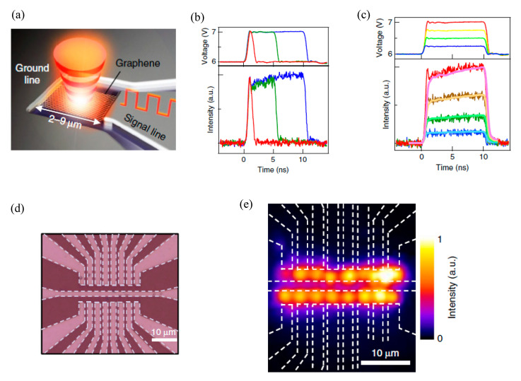
Figure 6.
(a) The structure of the graphene emitter black body emitter encapsulated with Al2O3, the CVD graphene was deposited on the square SiO2/Si substrate, which is attached with source and drain electrodes, where high modulation optical signal obtained by applying input signals. (b) Shows time resolve emission from the device under different pulse width (1, 5 and 10 ns) and voltage amplitude (6–7 V), (c) the time resolve emission from the device with a pulse width of 10 ns and amplitude 6 to 7 V. (d) The optical image of the highly integrated graphene 2 × 8 arrays thermal emitter with CVD graphene, with size 2 × 2 μm and pitch 3 μm. (e) NIR camera image of the light emission from the arrayed device, each array is connected to the same voltage (10 V), and series resistance is introduced with each array to demonstrate the relative uniform light emission from each device [62].

