Abstract
Plasmonic tip-sample junctions, at which the incident and scattered optical fields are localized and optimally enhanced, are often exploited to achieve ultrasensitive and highly spatially localized tip-enhanced Raman scattering (TERS). Recent work has demonstrated that the sensitivity and spatial resolution that are required to probe single molecules are attainable in such platforms. In this work, we observe and rationalize comparable TERS from few-layer WSe2 single crystals exfoliated onto Au- and Cr-coated Si substrates, using a plasmonic TERS probe excited with a 638 nm laser. Our experimental observations are supported by finite-difference time-domain simulations that illustrate that the attainable field enhancement factors at the Au–Au and Au–Cr tip-sample junctions are comparable in magnitude. Through a combined experimental and theoretical analysis, we propose that besides Au/Ag, several metallic substrates may be used to record bright TERS spectral images.
Graphical Abstract
INTRODUCTION
Tip-enhanced Raman scattering (TERS)1–4-based nanoscale chemical imaging is ideally suited for the characterization of low-dimensional molecular and material systems.5–9 This is especially the case for ultrathin 2D materials: a classical example of which is graphene sandwiched between a plasmonic TERS tip and a plasmonic substrate.10–17 Beyond carbon-based material systems, relatively recent initial observations of TERS18 as well as ‘tip-enhanced photoluminescence’ (TEPL)19 from MoS2 were immediately followed by numerous demonstrations in which nanoscale heterogeneities (down to 10 nm) in WS2,20 MoSe2,21 and WSe222 were directly visualized using these two complementary techniques. These results bolster the utility and promise of TERS and TEPL to advance the existing understanding of the fundamental properties of van-der-Waals layered materials.
In most of the existing TERS studies, both the probes and the substrates are made of single crystalline or polycrystalline gold or silver.5–16 The premise is that visible light irradiation excites a hybrid tip–substrate junction plasmon, which effectively leads to the extreme localization and enhancement of the incident and scattered optical fields.5–9 Indeed, a signal decrease of 1–2 orders of magnitude accompanies the switch from “gap mode”21,22 to tip-only TERS20 from well-defined 2D material systems, the dimensions of which are gauged through simultaneous/sequential topographic atomic force microscopy (AFM) measurements. In this regard, bright TERS requires highly optimized samples, which greatly limits the generality of the technique and necessitates transferring the sample, typically onto a gold or silver substrate. At the same time, unavoidable interactions between the sample and a substrate may unnecessarily obfuscate the information content in TERS spectra and images.23–25 In this work, we demonstrate that other metallic substrates may be used to achieve high TERS enhancement factors for 2D semiconductors and, as a result, high signal-to-noise TERS spectral images. The case is made through a comparison of the signal levels in hyperspectral TERS maps recorded from WSe2 single crystals exfoliated on Cr-on-Si vs Au-on-Si substrates.
EXPERIMENTAL SECTION
Substrate/Sample Preparation.
WSe2 flakes were grown using a chemical vapor transport method with SeBr4 as a transport agent. First, polycrystalline WSe2 powder was synthesized by reacting stoichiometric amounts of W (99.9%, Strem Chemicals) and Se (99.999%, Strem Chemicals) powders in a vacuum-sealed quartz ampule at 750 °C for 2 days followed by annealing at 850 °C for 3 days in the same ampule.1 Then, a quartz ampule containing ≈1 g of WSe2 charge and ≈0.1 g (5 mg/cm3) of SeBr4 transport agent (99%, Strem Chemicals) was sealed under a vacuum and placed in a horizontal quartz tube furnace. The growth lasted 90 h with the charge and growth zone temperatures set to 825 and 700 °C, respectively.
For TERS measurements, WSe2 flakes were mechanically exfoliated onto chromium and gold-coated silicon chips. The 30 nm thick Cr and Au films were deposited onto Si(100) substrates using the 4Wave dual chamber ion beam (Cr) and bias target (Au) cluster deposition system at the base pressure of 2.6 × 10⁻⁶ Pa (2 × 10⁻⁸ Torr). Prior to the Au film deposition, a 20 nm layer of Ti was deposited onto Si surface to promote good adhesion of Au.
TERS Measurements.
AFM characterization and TERS imaging were carried out in air on an OmegaScope-R system (Horiba Scientific), coupled to XploRA confocal Raman spectrometer (Horiba Scientific). A linearly polarized 638 nm laser (100 μW/μm2) was incident onto the sample through a 100x objective (Mitutoyo, NA = 0.7) at a 65° with respect to the surface normal. An OMNI-TERS AFM probe (silver coated, with a thin protective gold overlayer; k = 3 N/m, f = 73.5 kHz, APPNano, Horiba Scientific) was used to record the TERS maps shown herein, and the laser polarization was set along the long axis of the tip. A dedicated TERS imaging mode (SpecTop) was employed for fast and efficient TERS mapping. Using this mode, TERS signals are collected when the tip is in direct contact with the surface, with a typical force in the 2–10 nN range. A semicontact mode is used to move the sample relative to the tip (pixel to pixel) to preserve the sharpness and optical properties of the tip and to minimize the lateral forces that otherwise perturb the sample or contaminate the tip in conventional constant contact mode feedback.
Numerical Simulations.
Simulations were performed using a commercial FDTD package (Lumerical FDTD Solutions). The interaction of electromagnetic plane waves with the tip–surface construct (vide infra) is evaluated by iteratively solving finite-difference analogues of the time-dependent Maxwell equations. The calculations model a solid silver tip with a 50 nm radius that is coated with a 20 nm gold overlayer. The tip is positioned 4 nm above a surface composed of 30 nm-thick metallic films supported by a silicon substrate. For reference, we also consider the case of tip (same as above) atop an uncoated glass substrate. A Gaussian source centered at 638 nm illuminates the tip/surface structure at a 65° angle with respect to the surface normal through an air objective (NA = 0.7). Much like in the experiment, the incident light source is nominally polarized along the tip axis. The calculation outputs a three-dimensional surface of field enhancement which is then compared to the experiment. The dielectric permittivity of silver is obtained from Yang et al.,26 gold constants are obtained from Olmon et al.27 Other constants are otherwise sourced from Palik.28–30
RESULTS AND DISCUSSION
Our first task is to establish that we can directly compare TERS signals recorded from WSe2 flakes exfoliated onto Cr-on-Si and Au-on-Si substrates. To this end, freshly prepared samples were imaged. To set a baseline for our discussion, we begin with a brief exposition of the TERS spectral images of WSe2 on Au.
Few-layer WSe2 flakes (≈7 nm in height as measured through topographic AFM, Figure 1A,B) exhibit strong resonant TERS scattering following 638 nm excitation. It is important to note that the far field/diffraction-limited response is weak, approximately an order of magnitude lower than the near field signal, as evidenced through the observation of well-defined sharp edges of the WSe2 flake in the TERS map that correctly reproduce their analogues in the topographic image (Figure 1A and the inset of Figure 1C). If the far-field signal contribution was significant, the TERS map would exhibit more gradual, diffraction-limited (≈500 nm) transition at the edges of the flake. A detailed comparison between the far and near field components of the overall signal are provided in Figure S1. The enhanced resonant Raman spectra shown in Figure 1C exhibit the out-of-plane/in-plane A1g/E2g peak at around 250 cm−1 overlapping with the peak of the second order longitudinal acoustic phonon at M point 2LA(M) at 260 cm−1, as well as two weaker features at ≈130 and 395 cm−1, which correspond to the first and third order of longitudinal acoustic mode at M point LA(M) and 3LA(M) respectively.31
Figure 1.
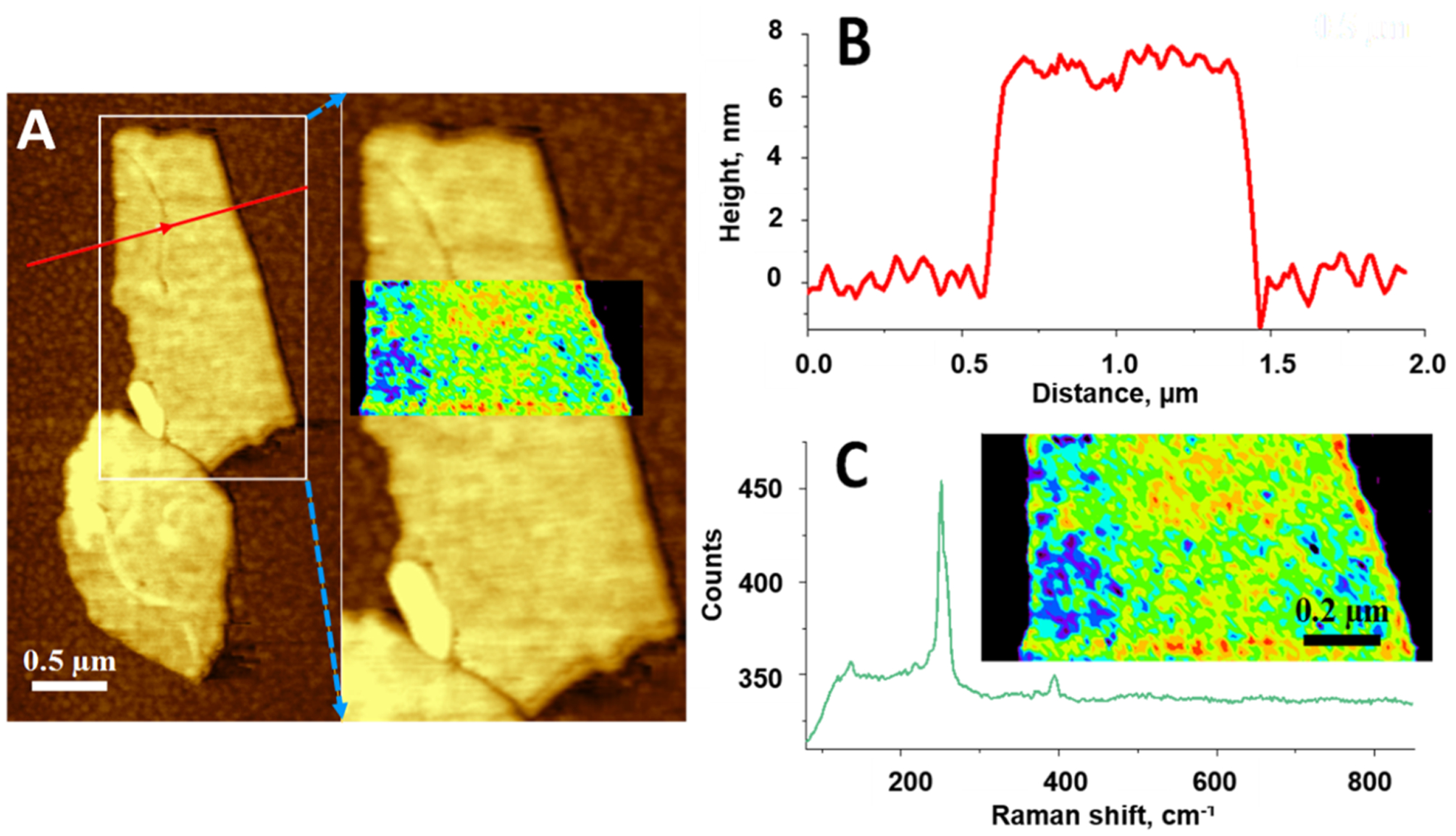
(A) Topographic AFM image of WSe2 flakes on an Au-on-Si substrate. The measured height of these flakes is about 7 nm and is uniform across the sheets, as illustrated by a cross-sectional height profile in panel B. Panel A also shows a 1.2 μm × 0.6 μm TERS image (88 pixels/line, 13.6 nm/pixel) where the intensity of the peaks within the 235–270 cm−1 range is overlaid over the topographic AFM image. The TERS image is expanded in the inset of panel C, which also shows the spatially averaged TERS spectra of WSe2 that exhibit the familiar resonant Raman response of this system following red-laser excitation. Rather sharp edges of the flake are evident in the TERS map, which is indicative of strong TERS enhancement and nearly pixel-limited spatial resolution.
WSe2 flakes that are comparable in their overall topographic features to the ones showed in Figure 1 were subsequently located on the Cr-on-Si substrate, see Figure 2, using the same TERS probe. Somewhat surprisingly, the TERS activity of these flakes were comparable to their Au-supported analogues. In terms of the characteristic spectral features, the longitudinal acoustic phonon peaks LA(M) (~130 cm−1), 2LA(M) (~260 cm−1), and 3LA(M) (~395 cm−1) are still observable, albeit exhibiting slightly less prominent relative intensities in these spectra (Figure 2D) as compared to their analogues on Au (Figure 1C). Note that the predominant A1g/E2g modes at 250 cm−1 are otherwise unscathed. These two observations suggest that the attainable TERS activities in the Au and Cr cases are not a result of significantly modified local chemical environments at the WSe2/Au interface in these two samples.
Figure 2.
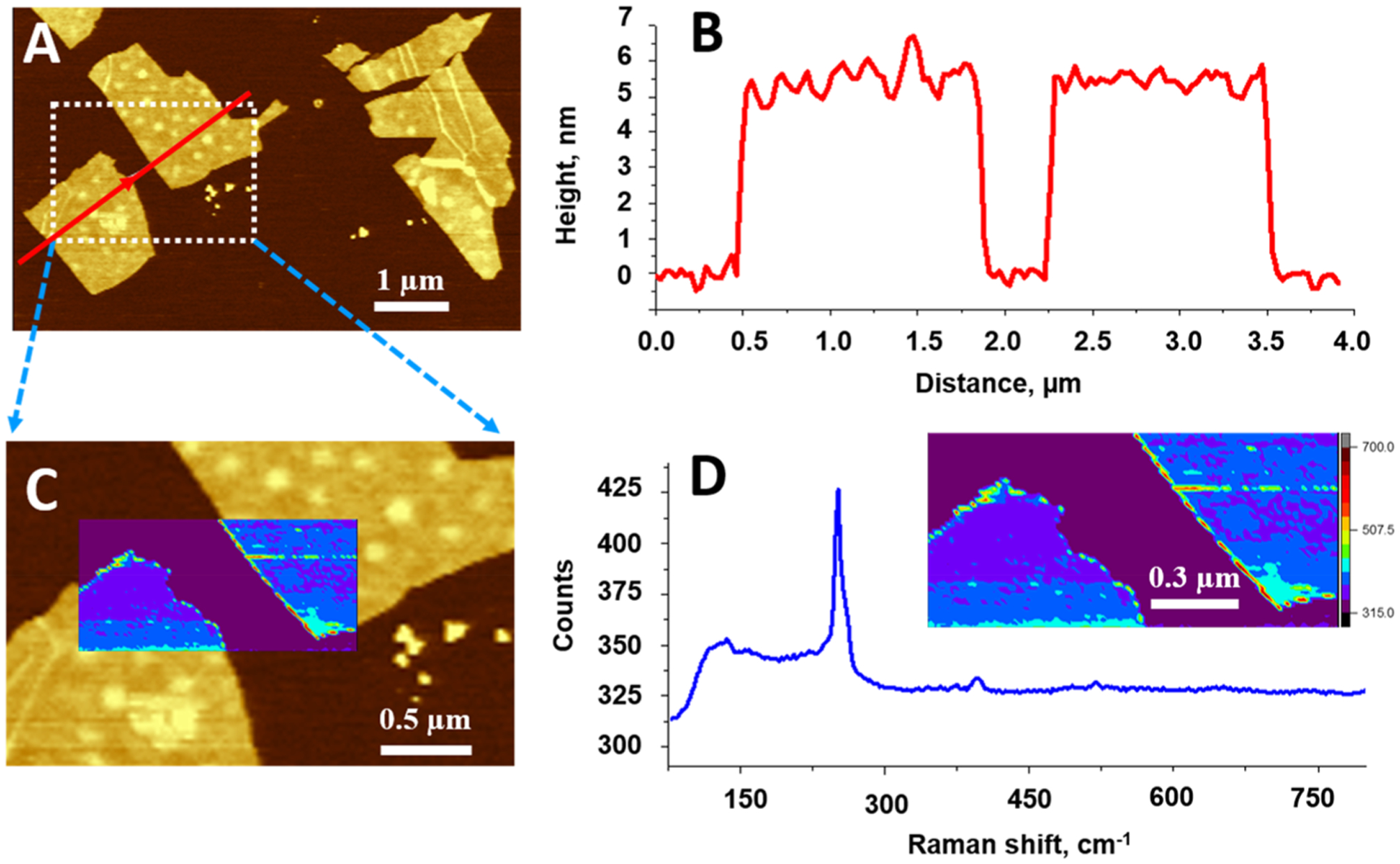
(A) Topographic AFM image of WSe2 flakes on a Cr-on-Si substrate. The measured height of these flakes is about 5.5 nm, and is uniform across the sheets, as illustrated by a cross-sectional height profile in panel B. (C) 1.5 μm × 0.75 μm TERS image (100 pixels/line, 15 nm/pixel) where the intensity of the peaks within the 235–270 cm−1 range is overlaid over the topographic image. The same image is expanded in the inset of panel D, which also shows a spatially averaged TERS spectrum of WSe2 that again exhibits the familiar resonant Raman response of this system following red-laser excitation. Much like in Figure 1, rather sharp edges of the flake are evident in the TERS map, which is indicative of strong TERS enhancement, pixel-limited spatial resolution, and a dim far field response.
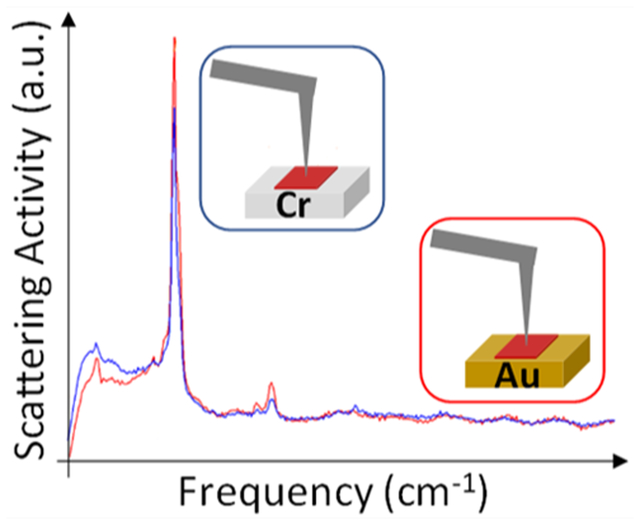
A more direct comparison between the TERS signals that were recorded from the two samples emphasizes the statement above; see Figure 3. Namely, the overall similarities between the (spatially averaged) TERS spectra of WSe2 on Au (red spectrum) and Cr (black trace) are evident. Interestingly, when the tip is in direct contact with the underlying metals 100–200 nm away from the edges of WSe2 crystals, (Au/Cr in green/blue, respectively), a much more pronounced TERS “background” is observed for the case of the plasmonic support. On the basis of prior analyses, we tentatively attribute this observation to electronic Raman scattering from nanometrically rough Au.32 Its absence in the case of Cr is intriguing and suggests that either (i) the difference in the surface roughness of the Cr and gold substrates (RMS 0.2 and 0.44 nm, correspondingly) is sufficient to affect the intensity of the background signal, or (ii) plasmonic modes in the visible (in the vicinity of the excitation wavelength) are prerequisite to the observation of backgrounds from imperfect mirrors/nanometrically roughened metals.
Figure 3.
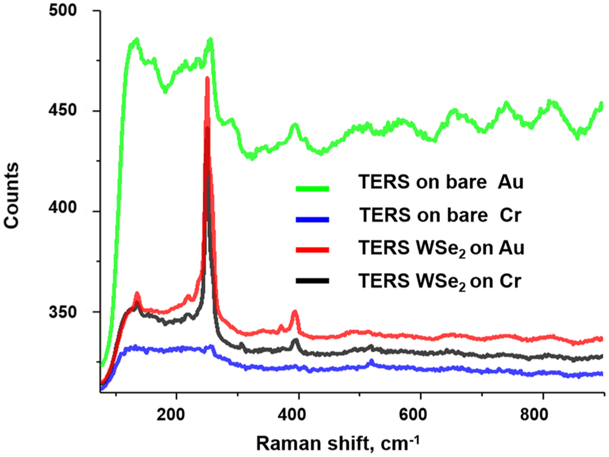
Comparison between the TERS signals averaged over a 150 × 150 nm area, obtained with the same TERS probe from WSe2 on Au (red) and Cr (black). The similarity between the two spectra in terms of the observable resonances and signal levels is noteworthy. Background signals observed when the tip was in direct contact with the metals in two cases are also shown. A significantly more intense gold (green) compared to chromium (blue) background is observed. See text for more details. Ripples in the spectra, particularly pronounced in the background signal on gold are an artifact caused by optical interference on the back-illuminated CCD sensor.
Despite the fact that the measured heights of the crystals on gold and chromium were close, 7 and 5.5 nm respectively, we expect that the mere difference in the thickness of the crystals might affect the intensity of the gap-mode TERS signal. In order to understand how the crystal thickness affects the intensity of TERS signal, we measured TERS response from WSe2 crystals of different heights exfoliated on gold (see Figure S2 in Supporting Information). As expected, the intensity of the TERS signal decreases with increasing thickness. Extrapolating the data from the graph in Figure S2, we can estimate that the thickness-adjusted intensity of WSe2 on chromium was about 70% of the signal on gold.
To ensure the generality of our observations, several WSe2 crystals on a Cr-on-Si substrate were imaged. TERS spectral images recorded from a strategically selected flake are shown in Figure 4. The crystal of interest features two distinct areas that exhibit apparent heights of ≈3 nm and ≈7 nm, respectively. Although both parts of the flake exhibit a pronounced TERS response, the thinner one also shows a PL peak, which is rigorously indicative of a WSe2 monolayer.19,22 This observation suggests that ≈2.3 nm of the measured apparent height of the flakes in the samples consists of a contamination layer that isolates the substrate from the WSe2 monolayer, an observation eluded to in a prior report.33 On this basis, we can re-estimate the number of layers in the imaged WSe2 flakes, where 3 and 7 nm apparent heights correspond to 1 and 6 WSe2 layers, respectively, taking into account an approximate thickness of a monolayer of 0.7 nm.
Figure 4.
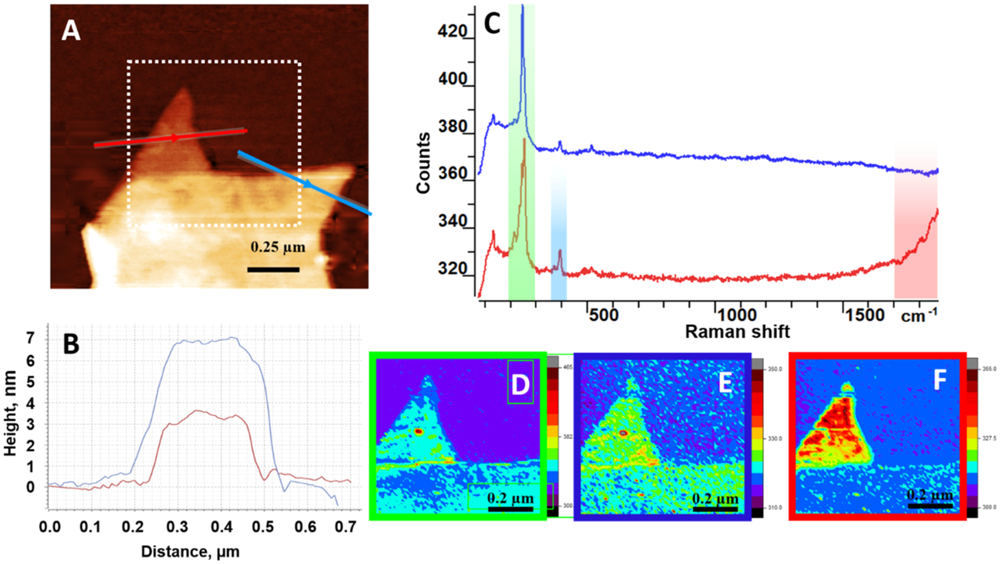
(A) Topographic AFM image of the WSe2 flake on Cr surface. (B) Corresponding profiles along the red and blue lines in panel A, featuring two distinct parts of the flake with approximate heights of 3 and 7 nm, respectively. (C) TERS/TEPL spectra from the 3 nm (red line) and 7 nm (blue line) thick areas, offset vertically by 50 counts for clarity. TERS (Panels D, E) and TEPL (panel F) maps from the square area, indicated by a dotted square in panel A. The spectral window for each map is: (D) from 195 to 295 cm−1 (green band in panel C), (E) from 360 to 420 cm−1 (blue band in panel C), (F) from 1700 to 1850 cm−1 (red band in panel C).
To further ensure reproducibility of the results obtained in the first round of measurements, we repeated the experiments on new set of WSe2 crystals exfoliated to gold and chromium. Even though in these samples we have not been able to locate crystals of similar height, the thickness-adjusted intensity of the TERS signal on chromium was found to be about 50% of corresponding signal on gold (see Figure S3 and related text in Supporting Information), which qualitatively agrees with the above-described results of our first round of measurements.
To rationalize our experimental observation of comparable TERS intensities from few-layer WSe2 single crystals exfoliated onto Au-on-Si and Cr-on-Si substrates, we performed finite-difference time-domain simulations; see Figure 5B–C. For reference, we also simulated the fields sustained at the apex when our plasmonic Au TERS probe is atop a glass substrate; see Figure 5A. We additionally performed predictive simulations that consider several other metallic substrates to assess the generality of our observations and analysis; see Figure 5D,E. Note that the general asymmetry in the field profiles shown in Figure 5 arises from the low-angle-of incidence of the incident microscopic laser field. For all metals tested, approaching the plasmonic tip toward the substrate leads to the confinement and enhancement of the electromagnetic field (Figure 5B–F). On the basis of our calculations, it is useful to comment on the attainable field enhancement factors. Assuming that all 4 electric fields involved in the TERS process are enhanced,34 the total TERS signal enhancement follows the (E/E0)4 law. In this case, all of the simulated plasmonic tip-metallic substrate constructs support enhancement factors that only differ by a single order of magnitude, i.e., in the ≈(1–9) × 105 range. This translates into comparable TERS signals for measurements performed on Au-on-Si vs Cr-on-Si substrates. In the absence of the underlying metallic support (Figure 5A), modest tip-only TERS would be expected, which is again consistent with prior observations.35 More generally, our simulations suggest that the choice of underlying metal (Cr, Au, Mg, Al, Ag) does not affect the overall TERS signals in practice. In this regard, our results are consistent with a previous report on TERS signals from aromatic molecules on metallic substrates.17 Ultimately, both the real and imaginary parts of the dielectric determine the overall field enhancement. As the real dielectric becomes less negative, the field enhancement increases until the imaginary part becomes appreciable.36 At the red excitation wavelength used, Cr has a larger imaginary dielectric constant but smaller real dielectric constant relative to gold, resulting in a similar field enhancement and therefore TERS signal.
Figure 5.
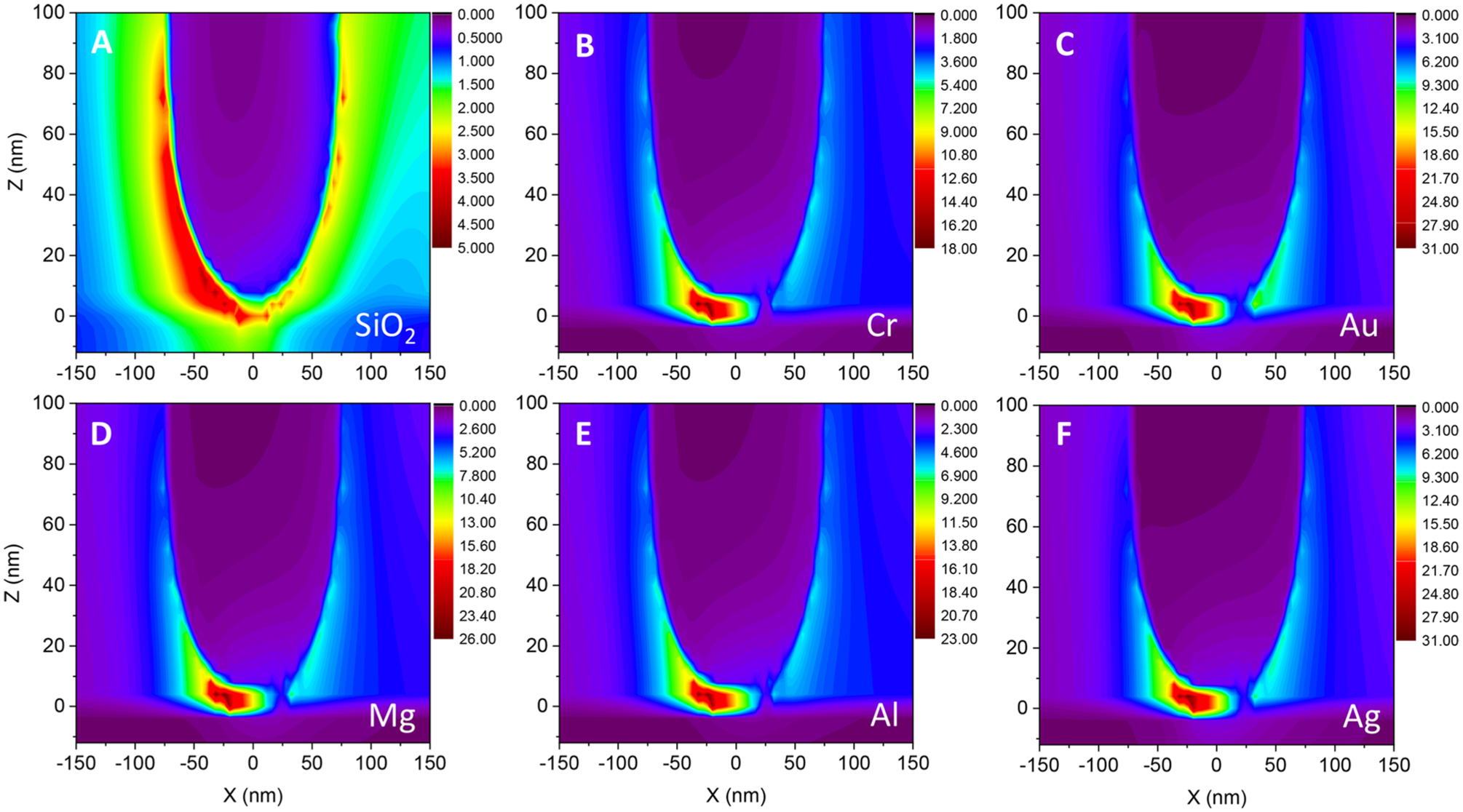
Electric field (E/E0) image slices in the XZ plane are shown in panels A (SiO2 substrate), B (Cr-on-Si), C (Au-on-Si), D (Mg-on-Si), E (Al-on-Si), and F (Ag-on-Si). As discussed in the experimental and theoretical section of this manuscript, the simulations emulate all aspects of the experiments, including the laser color/polarization/angle of incidence. Note that the laser is incident from left to right, which leads to the asymmetry in the field maps for all constructs used. See text for more details. Note the differences in the scale bar ranges in A–F.
CONCLUSIONS
The experimental results and theoretical analysis presented in this work reveal that bright TERS signals are attainable from analytes sandwiched between Au/Ag TERS probes and various visible light-reflecting metals. Namely, the choice of metallic substrate is not necessarily restricted to gold, silver, and other noble metals. Experimentally, this was demonstrated through TERS-based nanoscale chemical imaging of few-layer WSe2 single crystals exfoliated onto Au-on-Si and Cr-on-Si substrates. Unlike molecular reporters, where a plethora of effects can contribute to the variations in the recorded signal magnitudes, 2D materials are ideal targets for fundamental TERS studies. Finite-difference time-domain simulations corroborate our observables and further suggest that other metal substrates (including Mg, Al, and potentially other metallic mirrors) are expected to support TERS signals that are similar in magnitude to those reported herein. The prospect of utilizing several metallic substrates in TERS spectral imaging measurements should contribute to the growth and generality of this powerful nanoscale chemical imaging technique. The ability to utilize substrates other than Au and Ag may simplify general TERS sample preparation and expand the choice of substrates, which for some applications such as bioimaging, are currently restricted to Au.
Supplementary Material
ACKNOWLEDGMENTS
A.B. was supported in part by the Department of Energy’s (DOE) Office of Biological and Environmental Research Bioimaging Technology project #69212. A.K. acknowledges support through Horiba Instruments Inc. A.G.J. and P.Z.E. acknowledge support from the Laboratory Directed Research and Development Program at Pacific Northwest National Laboratory (PNNL). S.K. acknowledges support from the U.S. Department of Commerce, National Institute of Standards and Technology under the financial assistance award 70NANB18H155
Footnotes
Disclaimer: Certain commercial equipment, instruments, or materials are identified in this paper in order to specify the experimental procedure adequately. Such identification is not intended to imply recommendation or endorsement by the National Institute of Standards and Technology nor is it intended to imply that the materials or equipment identified are necessarily the best available for the purpose.
Contributor Information
Andrey Krayev, Horiba Instruments Inc., Novato, California 94949, United States.
Sergiy Krylyuk, Material Measurement Laboratory, National Institute of Standards and Technology, Gaithersburg, Maryland 20899, United States; Theiss Research, Inc., La Jolla, California 92037, United States.
Robert Ilic, Physical Measurement Laboratory, National Institute of Standards and Technology, Gaithersburg, Maryland 20899, United States.
Angela R. Hight Walker, Physical Measurement Laboratory, National Institute of Standards and Technology, Gaithersburg, Maryland 20899, United States.
Ashish Bhattarai, Physical Sciences Division, Pacific Northwest National Laboratory, Richland, Washington 99352, United States.
Alan G. Joly, Physical Sciences Division, Pacific Northwest National Laboratory, Richland, Washington 99352, United States.
Matěj Velický, Department of Chemistry and Chemical Biology, Cornell University, Ithaca, New York 14853, United States; School of Physics and Astronomy, University of Manchester, Manchester M13 9PL, United Kingdom.
Albert V. Davydov, Material Measurement Laboratory, National Institute of Standards and Technology, Gaithersburg, Maryland 20899, United States
Patrick Z. El-Khoury, Physical Sciences Division, Pacific Northwest National Laboratory, Richland, Washington 99352, United States.
REFERENCES
- (1).Anderson MS Locally Enhanced Raman Spectroscopy with an Atomic Force Microscope. Appl. Phys. Lett 2000, 76, 3130–3132. [Google Scholar]
- (2).Stockle RM; Suh YD; Deckert V; Zenobi R Nanoscale Chemical Analysis by Tip-Enhanced Raman Spectroscopy. Chem. Phys. Lett 2000, 318, 131–136. [Google Scholar]
- (3).Pettinger B; Schambach P; Villagomez CJ; Scott N Tip-Enhanced Raman Spectroscopy: Near-Fields Acting on a Few Molecules. Annu. Rev. Phys. Chem 2012, 63, 379–399. [DOI] [PubMed] [Google Scholar]
- (4).Stadler J; Schmid T; Zenobi R Developments in and Practical Guidelines for Tip-Enhanced Raman Spectroscopy. Nanoscale 2012, 4, 1856–1870. [DOI] [PubMed] [Google Scholar]
- (5).Zrimsek AB; Chiang NH; Mattei M; Zaleski S; McAnally MO; Chapman CT; Henry AI; Schatz GC; Van Duyne RP Single-Molecule Chemistry with Surface- and Tip-Enhanced Raman Spectroscopy. Chem. Rev 2017, 117, 7583–7613. [DOI] [PubMed] [Google Scholar]
- (6).Jiang N; Kurouski D; Pozzi EA; Chiang NH; Hersam MC; Van Duyne RP Tip-Enhanced Raman Spectroscopy: From Concepts to Practical Applications. Chem. Phys. Lett 2016, 659, 16–24. [Google Scholar]
- (7).Wang X; Huang SC; Huang TX; Su HS; Zhong JH; Zeng ZC; Li MH; Ren B Tip-Enhanced Raman Spectroscopy for Surfaces and Interfaces. Chem. Soc. Rev 2017, 46, 4020–4041. [DOI] [PubMed] [Google Scholar]
- (8).Richard-Lacroix M; Zhang Y; Dong ZC; Deckert V Mastering High Resolution Tip-Enhanced Raman Spectroscopy: Towards a Shift of Perception. Chem. Soc. Rev 2017, 46, 3922–3944. [DOI] [PubMed] [Google Scholar]
- (9).Verma P Tip-Enhanced Raman Spectroscopy: Technique and Recent Advances. Chem. Rev 2017, 117, 6447–6466. [DOI] [PubMed] [Google Scholar]
- (10).Park KD; Raschke MB; Atkin JM; Lee YH; Jeong MS Probing Bilayer Grain Boundaries in Large-Area Graphene with Tip-Enhanced Raman Spectroscopy. Adv. Mater 2017, 29, 1603601. [DOI] [PubMed] [Google Scholar]
- (11).Fang ZY; Thongrattanasiri S; Schlather A; Liu Z; Ma LL; Wang YM; Ajayan PM; Nordlander P; Halas NJ; de Abajo FJG Gated Tunability and Hybridization of Localized Plasmons in Nanostructured Graphene. ACS Nano 2013, 7, 2388–2395. [DOI] [PubMed] [Google Scholar]
- (12).Mertens J; et al. Controlling Subnanometer Gaps in Plasmonic Dimers Using Graphene. Nano Lett. 2013, 13, 5033–5038. [DOI] [PubMed] [Google Scholar]
- (13).Fang ZY; Liu Z; Wang YM; Ajayan PM; Nordlander P; Halas NJ Graphene-Antenna Sandwich Photodetector. Nano Lett. 2012, 12, 3808–3813. [DOI] [PubMed] [Google Scholar]
- (14).Stadler J; Schmid T; Zenobi R Nanoscale Chemical Imaging of Single-Layer Graphene. ACS Nano 2011, 5, 8442–8448. [DOI] [PubMed] [Google Scholar]
- (15).Domke KF; Pettinger B Tip-Enhanced Raman Spectroscopy of 6h-Sic with Graphene Adlayers: Selective Suppression of E1Modes. J. Raman Spectrosc 2009, 40, 1427–1433. [Google Scholar]
- (16).Beams R Tip-Enhanced Raman Scattering of Graphene. J. Raman Spectrosc 2018, 49, 157–167. [Google Scholar]
- (17).Stadler J; Oswald B; Schmid T; Zenobi R Characterizing Unusual Metal Substrates for Gap-Mode Tip-Enhanced Raman Spectroscopy. J. Raman Spectrosc 2013, 44, 227–233. [Google Scholar]
- (18).He Z; Voronine DV; Sinyukov AM; Liege ZN; Birmingham B; Sokolov AV; Zhang ZR; Scully MO Tip-Enhanced Raman Scattering on Bulk Mos2 Substrate. IEEE J. Sel. Top. Quantum Electron 2017, 23, 113. [Google Scholar]
- (19).Bao W; Borys NJ; Ko C; Suh J; Fan W; Thron A; Zhang Y; Buyanin A; Zhang J; Cabrini S; Ashby PD; Weber-Bargioni A; Tongay S; Aloni S; Ogletree DF; Wu J; Salmeron MB; Schuck PJ Visualizing Nanoscale Excitonic Relaxation Properties of Disordered Edges and Grain Boundaries in Monolayer Molybdenum Disulfide. Nat. Commun 2015, 6, 8993 DOI: 10.1038/ncomms8993. [DOI] [PMC free article] [PubMed] [Google Scholar]
- (20).Kastl C; Chen CT; Kuykendall T; Shevitski B; Darlington TP; Borys NJ; Krayev A; Schuck PJ; Aloni S; Schwartzberg AM The Important Role of Water in Growth of Monolayer Transition Metal Dichalcogenides. 2D Mater. 2017, 4, 021024. [Google Scholar]
- (21).Smithe KKH; et al. Nanoscale Heterogeneities in Monolayer MoSe2 Revealed by Correlated Scanning Probe Microscopy and Tip-Enhanced Raman Spectroscopy. ACS Applied Nano Materials 2018, 1, 572–579. [Google Scholar]
- (22).Park KD; Khatib O; Kravtsov V; Clark G; Xu X; Raschke MB Hybrid Tip-Enhanced Nanospectroscopy and Nanoimaging of Monolayer Wse2 with Local Strain Control. Nano Lett. 2016, 16, 2621–7. [DOI] [PubMed] [Google Scholar]
- (23).Bhattarai A; El-Khoury PZ Imaging Localized Electric Fields with Nanometer Precision through Tip-Enhanced Raman Scattering. Chem. Commun 2017, 53, 7310–7313. [DOI] [PubMed] [Google Scholar]
- (24).Bhattarai A; Krayev A; Temiryazev A; Evplov D; Crampton KT; Hess WP; El-Khoury PZ Tip-Enhanced Raman Scattering from Nanopatterned Graphene and Graphene Oxide. Nano Lett. 2018, 18, 4029–4033. [DOI] [PubMed] [Google Scholar]
- (25).El-Khoury PZ; Abellan P; Gong Y; Hage FS; Cottom J; Joly AG; Brydson R; Ramasse QM; Hess WP Visualizing Surface Plasmons with Photons, Photoelectrons, and Electrons. Analyst 2016, 141, 3562–3572. [DOI] [PubMed] [Google Scholar]
- (26).Yang HHU; D’Archangel J; Sundheimer ML; Tucker E; Boreman GD; Raschke MB Optical Dielectric Function of Silver. Phys. Rev. B: Condens. Matter Mater. Phys 2015, 91, 235137 DOI: 10.1103/PhysRevB.91.235137. [DOI] [Google Scholar]
- (27).Olmon RL; Slovick B; Johnson TW; Shelton D; Oh SH; Boreman GD; Raschke MB Optical Dielectric Function of Gold. Phys. Rev. B: Condens. Matter Mater. Phys 2012, 86, 235147 DOI: 10.1103/PhysRevB.86.235147. [DOI] [Google Scholar]
- (28).List of Contributors for Vol. Iii In Handbook of Optical Constants of Solids, Palik ED, Ed. Academic Press: Burlington, 1997; pp xiii–xv. [Google Scholar]
- (29).List of Contributors for Vol. I In Handbook of Optical Constants of Solids, Palik ED, Ed. Academic Press: Burlington, 1997; pp xv–xvi. [Google Scholar]
- (30).List of Contributors for Vol. Ii In Handbook of Optical Constants of Solids, Palik ED, Ed. Academic Press: Burlington, 1997; pp xv–xviii. [Google Scholar]
- (31).del Corro E; Terrones H; Elias A; Fantini C; Feng SM; Nguyen MA; Mallouk TE; Terrones M; Pimenta MA Excited Excitonic States in 1l, 2l, 3l, and Bulk Wse2 Observed by Resonant Raman Spectroscopy. ACS Nano 2014, 8, 9629–9635. [DOI] [PubMed] [Google Scholar]
- (32).Hugall JT; Baumberg JJ Demonstrating Photo-luminescence from Au Is Electronic Inelastic Light Scattering of a Plasmonic Metal: The Origin of Sers Backgrounds. Nano Lett. 2015, 15, 2600–2604. [DOI] [PMC free article] [PubMed] [Google Scholar]
- (33).Rosenberger MR; Chuang HJ; McCreary KM; Hanbicki AT; Sivaram SV; Jonker BT Nano-″Squeegee″ for the Creation of Clean 2d Material Interfaces. ACS Appl. Mater. Interfaces 2018, 10, 10379–10387. [DOI] [PubMed] [Google Scholar]
- (34).Bhattarai A; Joly AG; Hess WP; El-Khoury PZ Visualizing Electric Fields at Au(111) Step Edges Via Tip-Enhanced Raman Scattering. Nano Lett 2017, 17, 7131–7137. [DOI] [PubMed] [Google Scholar]
- (35).Bhattarai A; El-Khoury PZ Imaging Localized Electric Fields with Nanometer Precision through Tip-Enhanced Raman Scattering. Chem. Commun 2017, 53, 7310–7313. [DOI] [PubMed] [Google Scholar]
- (36).Zhang WH; Cui XD; Martin OJF Local Field Enhancement of an Infinite Conical Metal Tip Illuminated by a Focused Beam. J. Raman Spectrosc 2009, 40, 1338–1342. [Google Scholar]
Associated Data
This section collects any data citations, data availability statements, or supplementary materials included in this article.


