

Abstract
Electron-enhanced atomic layer deposition (EE-ALD) was used to deposit boron nitride (BN) thin films at room temperature and 100 °C using sequential exposures of borazine (B3N3H6) and electrons. Electron-stimulated desorption (ESD) of hydrogen surface species and the corresponding creation of reactive dangling bonds are believed to facilitate borazine adsorption and reduce the temperature required for BN film deposition. In situ ellipsometry measurements showed that the BN film thickness increased linearly versus the number of EE-ALD cycles at room temperature. Maximum growth rates of ~3.2 Å/cycle were measured at electron energies of 80–160 eV. BN film growth was self-limiting versus borazine and electron exposures, as expected for an ALD process. The calculated average hydrogen ESD cross section was σ = 4.2 × 10⁻¹⁷ cm2. Ex situ spectroscopic ellipsometry measurements across the ~1 cm2 area of the BN film defined by the electron beam displayed good uniformity in thickness. Ex situ X-ray photoelectron spectroscopy and in situ Auger spectroscopy revealed high purity, slightly boron-rich BN films with C and O impurity levels <3 at. %. High-resolution transmission electron microscopy (HR-TEM) imaging revealed polycrystalline hexagonal and turbostratic BN with the basal planes approximately parallel to the substrate surface. Ex situ grazing incidence X-ray diffraction measurements observed peaks consistent with hexagonal BN with domain sizes of 1–2 nm. The BN EE-ALD growth rate of ~3.2 Å/cycle is close to the distance of 3.3 Å between BN planes in hexagonal BN. The growth rate and HR-TEM images suggest that approximately one monolayer of BN is deposited for every BN EE-ALD cycle. TEM and scanning TEM/electron energy loss spectroscopy measurements of BN EE-ALD on trenched wafers also showed preferential BN EE-ALD on the horizontal surfaces. This selective deposition on the horizontal surfaces suggests that EE-ALD may enable bottom-up filling of vias and trenches.
Graphical Abstract
1. INTRODUCTION
Electron-enhanced processes, such as electron-beam-induced deposition employing high energy electrons at >1 keV, can dramatically reduce the temperatures required for thin-film growth.1,2 The temperature reduction occurs because the high-energy electrons, or the low-energy secondary electrons at <100 eV generated by the interaction between the high-energy electrons and the substrate, can dissociate molecular precursors and form reactive species that deposit on the substrate.3,4 Without the electron enhancement, thin-film growth typically relies on thermal pathways for dissociation or desorption that requires much higher temperatures. Low-energy electrons can also lead to electron attachment and dissociation products that extract surface species and create reactive “dangling bonds” that facilitate the adsorption of molecular precursors.3,5
Electron-enhanced thin-film growth has been demonstrated previously for the deposition of polycrystalline GaN at room temperature.6 The polycrystalline GaN films were deposited using sequential surface reactions, similar to atomic layer deposition (ALD) processes,7 using Ga(CH3)3 (trimethylgallium), NH3 (ammonia), and electron exposures as the reactants. Hydrogen radical beam exposures were employed after the Ga(CH3)3 exposures to replace the CH3 groups with H surface species. The electron exposures removed surface hydrogen by electron-stimulated desorption (ESD). GaN growth rates of 1.3 Å/cycle were observed at room temperature at electron energies of 50 eV.6 The GaN growth rates were higher for larger electron fluxes.6
Amorphous Si films were also deposited by electron-enhanced ALD (EE-ALD) using sequential surface reactions with Si2H6 (disilane) and electron exposures as the reactants.8 The electron exposures removed surface hydrogen by hydrogen ESD. Si growth rates of 0.3 Å/cycle were measured at room temperature at electron energies of 100 eV.8 The Si growth was self-limiting versus Si2H6 dose pressures at constant Si2H6 exposure times for fixed electron exposure times. The Si growth was also self-limiting versus electron exposure times for fixed Si2H6 exposures. In addition, changes in the silicon growth rate were observed at electron energies corresponding with Si core-level energies.8
In this paper, boron nitride (BN) EE-ALD is examined using borazine (B3N3H6) and electrons as the reactants. BN is found in many forms such as hexagonal, cubic, and wurtzite BN. Hexagonal and cubic BN are analogous to graphite and diamond, respectively. Hexagonal BN is an insulating material with the same sp2-hybridized layer structure as graphene. Hexagonal BN is known for its high thermal stability and chemical inertness. 2D materials such as graphene can be grown on hexagonal BN.9,10 Monolayers of hexagonal BN are also used as the dielectric layer in field-effect transistors.11–13 Cubic BN is known for its high hardness and high elastic modulus.
The growth of hexagonal BN films usually requires very high temperatures. The standard technique for hexagonal BN growth is chemical vapor deposition (CVD) at temperatures of 800–1000 °C.14,15 Some lower temperature BN CVD processes are employed at 400 °C. However, these BN CVD films generally require a post-deposition annealing process at 1000 °C.16 BN ALD has been defined using BCl3 and NH3 as the precursors at deposition temperatures of 225–325 °C.17–19 BN ALD has also been accomplished using BBr3 and NH3 as the reactants.20 Higher temperatures of 750 °C were required to obtain the turbostratic structure.20 The crystallographic order was less for films deposited at 400 °C.20 Electron beams have also been employed to ionize or excite borazine to facilitate BN CVD at ~700–800 °C.21
The reduction in the deposition temperature for BN film growth using EE-ALD is achieved by ESD of hydrogen from the surface.22,23 ESD can occur through several different processes including the Menzel–Gomer–Redhead and Knotek–Feibelman mechanisms.24–27 The Menzel–Gomer–Redhead mechanism involves the excitation of a bonding orbital electron into an antibonding state that results in the dissociation of the bond and desorption of a surface species. The Knotek–Feibelman mechanism is an Auger process where a core-binding electron is displaced by the incident electron flux. A valance level electron loses energy and falls into the resulting hole and another valance electron absorbs the lost energy, leading to the desorption of a surface species. The ESD of hydrogen results in the creation of highly reactive “dangling bond” sites where precursors can be absorbed with little to no activation barrier.
BN EE-ALD films were grown using sequential cycles of borazine (B3N3H6) and low-energy electron exposures at 27 °C (room temperature) and 100 °C using electron energies from 50 to 450 eV. BN film growth was characterized by in situ four-wavelength ellipsometry, Auger spectroscopy, and mass spectrometry. The thickness and crystallinity of these BN films was studied using a variety of ex situ techniques including spectroscopic ellipsometry (SE), grazing incidence X-ray diffraction (GIXRD), X-ray photoelectron spectroscopy (XPS), and transmission electron microscopy (TEM). BN EE-ALD films were also deposited on trenched wafers to evaluate EE-ALD on high aspect ratio structures. These studies determined if EE-ALD could display area-selective deposition by depositing preferentially on horizontal surfaces. This ability of EE-ALD could enable the bottom-up filling of other materials, such as metals, in trenches or vias during semiconductor fabrication.
2. EXPERIMENTAL SECTION
2.1. Vacuum Chamber.
BN EE-ALD films were grown at room temperature and 100 °C in an ultrahigh vacuum (UHV) chamber that has been described previously.6,8 This UHV apparatus is defined by a sample load lock and a main vacuum chamber that is pumped with an ion pump and a turbomolecular pump. In addition, the apparatus also includes a sample analysis chamber containing an Auger electron spectroscopy (AES) spectrometer. The sample analysis chamber is pumped by an ion pump. The main chamber contains an electron flood gun (model FRA-2×1–2, Kimball Physics Inc.) for the electron-enhanced ALD experiments.28 The configuration of this electron flood gun is the same as described earlier for the Si EE-ALD experiments.8 The main chamber is also equipped with a mass spectrometer (PrismaPlus QMG 220, Pfeiffer Vacuum) for gas analysis and hot cathode and cold cathode pressure gauges for pressure measurement. The sample analysis chamber also includes a hot cathode pressure gauge.
2.2. Growth Procedure.
BN films where grown using borazine (B3N3H6; >95%, Gelest). Immediately prior to each set of EE-ALD reactions, the borazine bubbler was frozen with liquid nitrogen, and the remaining gases in the line were pumped out prior to thawing the borazine. This procedure was repeated in triplicate to ensure the reactant purity because borazine is prone to degradation. Borazine undergoes dehydropolymerization at temperatures >70 °C16,29 and can further decompose to BN and hydrogen gas.16
Films were deposited on boron-doped Si(111) substrates (Silicon Valley Microelectronics, Inc.). Prior to loading in the reaction chamber, the substrates were rinsed with acetone and methanol and submerged in Nano-Strip (Cyantec Corporation) for 3 min to remove surface contaminants. The silicon native oxide was etched, and the silicon surface was passivated with hydrogen by exposure to dilute hydrofluoric acid (50:1 H2O/HF) for 2 min.
The substrates were loaded into the load lock chamber, and the background pressure was reduced to 1 × 10⁻⁶ Torr. The load lock chamber and the substrate were irradiated for 30 min using UV lamps (RBD Instruments) to desorb water from the substrate surface and chamber walls. After the pressure in the load lock chamber was reduced to approximately 1 × 10⁻⁸ Torr, the substrate and the sample stage were transferred into the main chamber. The substrate and the main chamber were again irradiated with UV light for 30 min.
After irradiation, the substrate was transferred to the analysis chamber and exposed to hydrogen radicals created by the hydrogen atom beam source (MBE-Komponenten GmbH) using hydrogen gas (H2; research grade, Airgas) at 1 × 10⁻⁵ Torr for 30 min. The hydrogen radical flux at the surface was estimated to be 5 × 10¹⁵ H atoms cm−2 s−1. Samples were then returned to the main chamber for film growth. The EE-ALD reaction sequence was initiated after the main chamber reached a base pressure of 5 × 10⁻¹⁰ Torr.
A typical EE-ALD reaction sequence consisted of an electron gun exposure at 100 eV for 240 s with an electron emission current of 300 μA followed by a 15 s purge. The electron current on the sample was ~60% of the electron emission current. The electron beam area on the sample was ~1 cm2. A borazine exposure of approximately 7 × 10⁻² Torr s was then introduced into the chamber followed by a 150 s purge. Three in situ ellipsometry scans of 1 s each were recorded 120 s into the purge to determine the BN film thickness. Another 50 s was required for the electron gun filament to warm up to the emission temperature. This sequence was then repeated for the desired number of cycles. Approximately 7.5 min was required to complete one full BN EE-ALD cycle.
2.3. In Situ Film Analysis.
The main reaction chamber was equipped with a variety of in situ analysis techniques to observe film growth. Film thickness was determined with a four-wavelength ellipsometer (FS-1, Film Sense). An initial baseline scan of the substrate was recorded prior to the reactions. Film growth was modeled using a Cauchy model. During growth, three consecutive 1 s scans were collected during the purge 120 s after the borazine exposure. Growth rates were calculated by the film thicknesses measured during 10 consecutive reaction cycles.
In situ film composition was measured by AES using a microcylindrical mirror analyzer (microCMA) Auger spectrometer (RBD Instruments). The microCMA Auger spectrometer scanned a kinetic energy range of 30–930 eV with a step size of 1 eV. The beam potential was 3 kV with a filament current of 1.05 A. The AES data were collected and processed using CMapp (RBD Instruments) software.
Additionally, an in situ mass spectrometer (PrismaPlus QMG 220M, Pfeiffer Vacuum Inc.) was available for identification of gaseous reaction products. The mass spectrometer could measure mass signals up to m/z = 200 amu. The mass spectrometer also had an internal ion current to pressure calibration that allowed partial pressures to be estimated from ion currents.
2.4. Ex Situ Film Analysis.
The BN films were analyzed using a variety of ex situ techniques. The film thickness was determined using a spectroscopic ellipsometer (model M-2000, J.A. Woollam Co., Inc.) equipped with a focusing probe that reduced the spot size to ~300–400 μm. This small spot size allowed for spatial mapping of the BN growth area. Data were collected at incident angles of 65° and 70°. The SE data were fit with a B-spline model using CompleteEase (J.A Woollam Co., Inc.) software.
The film composition was determined by XPS analysis using an X-ray photoelectron spectrometer (PHI 5600). The spectrometer used a monochromatic Al Kα source at 1486.6 eV. The pass energy was 29.35 eV, and the step size was 0.25 eV. An electron beam neutralizer was used during the XPS measurements. XPS depth profiling and surface carbon removal were conducted using argon ion sputtering. The XPS data were collected using Auger Scan (RBD Instruments) software. The XPS data were analyzed in CASA XPS (Casa Software Ltd.) software.
The BN films were studied using GIXRD to determine if the films were crystalline. These GIXRD studies were performed with an X-ray diffractometer (D1 System, Bede Scientific Inc.). The GIXRD utilized Cu Kα irradiation at an incidence angle of 0.3°. Forward recoil elastic spectroscopy (FRES) was performed at the University of Minnesota Characterization Facility. The FRES results were collected with an incident ion beam of 3 MeV He+. The spot size was reduced to 1 mm2 normal to the source with an incidence angle of 75° on the sample.
The specimen for TEM examination was prepared by focused ion beam (FIB) milling. Protective metal layers (Ni and Pt) were first deposited on the surface. Subsequently, a Gaion beam was used to prepare a thin lamella at 30 kV and then at 5 kV. Damage induced by the FIB preparation was removed by subsequent Ar milling at 900 eV and then at 500 eV. High-resolution TEM (HR-TEM) phase contrast images were then recorded at 200 kV with the lamella aligned to the Si[112] zone axis.
The trenched sample for TEM analysis was prepared using a FEI Helios Duel Beam FIB system. Elemental mapping of the trenched sample was performed with a JEOL ARM 200 kV Scanning TEM (STEM) system equipped with a Gatan Quantum electron energy loss spectroscopy (EELS) spectrometer. The map area was defined in a STEM/high-angle annular dark field image. Elemental maps were extracted pixel by pixel from the EELS spectra collected in the map area.
Raman spectra were collected with an InVia Confocal Raman microscope (Renishaw) using a laser with a wavelength of 785 nm. The Raman data were processed with WiRE (Renishaw) software. Fourier transform infrared (FTIR) spectra were collected using a Bruker Tensor 27 spectrometer with a deuterated triglycine sulfate detector in the transmission mode. Data were collected between 4000 and 1000 cm−1 and processed using OPUS (Bruker) software.
3. RESULTS AND DISCUSSION
3.1. In Situ Film Growth and Characterization.
Growth of the BN EE-ALD films was studied with in situ four-wavelength ellipsometry. Figure 1 displays the growth of BN EE-ALD films at electron energies of 120, 300, and 400 eV. Linear BN growth versus number of BN EE-ALD cycles was observed at the various electron energies. Initial film deposition experienced nucleation delays of ~20 cycles on the Si(111) substrates. The film growth was then consistently observed to be linear versus number of BN EE-ALD cycles. The results in Figure 1 were collected on a previously grown BN EE-ALD film to remove nucleation effects. The borazine exposure was 7 × 10⁻² Torr s, and the electron emission current was 300 μA for 240 s. All reaction parameters were within the self-limiting behavior regimes.
Figure 1.

Film thickness versus cycle number for BN EE-ALD at three different electron energies. Borazine exposure was 7 × 10⁻² Torr s. Electron exposure was defined by an electron emission current of 300 μA for 240 s.
Figure 1 shows that the observed BN growth per cycle (GPC) was linear at 3.0 Å/cycle at an electron energy of 120 eV. When the electron energy was increased to 300 eV, the growth rate decreased to 2.5 Å/cycle. The growth rate decreased further to 2.0 Å/cycle at an electron energy of 400 eV. These decreases in the GPC at higher electron energies may result from competitive etch processes becoming more prominent and acting to reduce the overall BN growth rate.6 However, mass spectrometry studies did not observe any gas phase species that may result from BN etching during the electron exposure periods. Mass spectrometry studies did detect an increase in the m/z = 2 signal. This increase in H2 gas phase species is consistent with hydrogen ESD as the mechanism for BN film growth.
Figure 2 displays the BN GPC versus the electron energy. No film growth was observed with an electron energy of 0 eV. A film growth threshold occurred between 0 and 40 eV. The growth in the energy region between 0 and 40 eV could not be effectively probed because of limitations with the cycling of the electron flood gun. Earlier hydrogen ESD studies from Si(001) surfaces observed a threshold at 23 eV.22 In addition, previous Si EE-ALD growth studies observed an energy threshold at ~25 eV.8
Figure 2.

GPC versus electron energy for BN EE-ALD. Borazine exposure was 7 × 10⁻² Torr s. Electron exposure was defined by an electron emission current of 300 μA for 240 s.
Figure 2 shows a plateau in the GPC at ~3.0 Å/cycle between 80 and 160 eV. At electron energies >160 eV, the growth rate began to display a reduction. This decrease in GPC may be attributed to a change in the hydrogen ESD cross section or an increase in competitive etch processes.6 The growth rate is 1.5 Å/cycle at electron energies of 440 eV. At even higher electron energies, the competitive etch processes may remove any BN and lead to no BN film growth.
The self-limiting behavior of BN film growth was studied with respect to each reaction parameter to confirm the growth characteristics of this BN EE-ALD technique. Each study was performed with all reaction parameters, aside from the parameter of interest, held constant under self-limiting conditions. Additionally, each study was performed at 27 °C on a previously deposited BN film to avoid nucleation delays.
Figure 3 shows the BN GPC versus the borazine exposure. The BN GPC increases with borazine exposure and reaches the self-limiting behavior at borazine exposures >7 × 10⁻² Torr s. The maximum growth rate was found to be ~3.0 Å/cycle at self-limiting growth conditions. No growth was observed without a borazine exposure even with repeated electron exposures.
Figure 3.

GPC versus borazine exposure. Electron energy was 100 eV. Electron exposure was defined by an electron emission current of 300 μA for 240 s.
Figure 4 demonstrates that the self-limiting behavior was also observed with respect to electron exposure time for exposures greater than 240 s at an electron emission current of 300 μA. No growth occurred without an electron exposure. The maximum GPC was found to be ~3.2 Å/cycle. The results in Figure 4 can be used to calculate the hydrogen ESD cross section from the GPC versus the electron exposure time at an electron energy of 100 eV. This derivation of the hydrogen ESD cross section assumes that BN film growth is proportional to the dangling bond coverage following hydrogen ESD.
Figure 4.

GPC versus electron exposure. Borazine exposure was 7 × 10⁻² Torr s. Electron energy was 100 eV. Electron emission current was 300 μA. Solid line shows fit to data to determine the hydrogen ESD cross section.
If the BN EE-ALD growth rate is proportional to the dangling bond coverage, the GPC can be derived as follows:8,30,31
| (1) |
In eq 1, GPC is the BN GPC, α represents the maximum BN growth rate assuming ideal conditions, and τ is the time constant, in seconds. The experimental results in Figure 4 can be fit with eq 1. This fit results in τ = 72.7 s. The definition of τ can be rearranged to yield the hydrogen ESD cross-section equation
| (2) |
In eq 2, σ is the total ESD cross section (cm2) and Φ is the electron flux across the surface (e/cm2 s). The electron flux is defined as
| (3) |
In this equation, I is the electron current on the sample, A is the electron beam area, and e is the charge of an electron. For this experiment, I = 180 μA and A = 1 cm2. The τ from the fit of the experimental results in Figure 4, together with these experimental parameters, yields a hydrogen ESD cross section at 100 eV of σ = 1.2 × 10⁻¹⁷ cm2.
Figure 5 demonstrates that the BN EE-ALD film growth was also self-limiting for electron emission currents greater than 100 μA. No film growth was observed without electron exposures. The maximum GPC was ~3.2 Å/cycle. Figure 5 shows that a slight decrease in the BN growth rate was observed at an electron emission current of 500 μA. Electron emission currents greater than 500 μA were not feasible because of limitations of the electron gun.
Figure 5.

GPC versus electron emission current. Borazine exposure was 7 × 10⁻² Torr s. Electron exposure was defined by electron emission current of 300 μA for 240 s. Solid line shows fit to data to determine the hydrogen ESD cross section.
The BN GPC versus electron emission current in Figure 5 can also be fit to derive a hydrogen ESD cross section. By combining eqs 1–3, the GPC can be written as:
| (4) |
The fit of this expression to the points in Figure 5 yields a hydrogen ESD cross section of σ = 4.8 × 10⁻¹⁷ cm2. This hydrogen ESD cross section is four times larger than the hydrogen ESD cross section obtained from Figure 4.
3.2. Growth Conformality.
Figure 6 shows a picture of the BN EE-ALD film growth on the Si(111) substrate. The electron flood gun acts as a point source of electrons located ~3 cm away and at close to normal incidence to the substrate surface. The film growth is observed to be approximately circular with an area of ~1 cm2. This shape is characteristic of the Gaussian distribution of electrons originating from the electron flood gun. There is no visible BN film growth outside the electron flux region. The film pictured in Figure 6 was grown using 500 EE-ALD cycles at 27 °C on the Si(111) substrate. Self-limiting parameters were used for the deposition with borazine exposures of 7 × 10⁻² Torr s, an electron energy of 100 eV, and electron exposures defined by an electron emission current of 300 μA for 240 s.
Figure 6.

Picture of the BN film grown by EE-ALD at 27 °C on the Si(111) substrate. The film was grown using 500 EE-ALD cycles with borazine exposures of 7 × 10⁻² Torr s, electron energy of 100 eV, and electron exposures defined by an electron emission current of 300 μA for 240 s.
Ex situ SE was used to measure the spatial profile of the BN growth area. This spatial profile is displayed as the points in Figure 7. The film thickness is uniform across the deposition area with a thickness of ~150 nm. The spatial profile displayed in Figure 7 is from the same sample shown in Figure 6. The calculated BN EE-ALD growth rate obtained from the film thickness is ~3.0 Å/cycle. This growth rate is consistent with the growth rates observed for BN EE-ALD at 100 eV under self-limiting growth conditions, as shown in Figures 2–5.
Figure 7.

Spatial profile of the BN EE-ALD growth area measured by SE for the BN film shown in Figure 6. Solid lines show fit to points assuming a Gaussian electron beam spatial profile to determine the hydrogen ESD cross section.
There is a variation in film thickness of ~10 Å across the top of the growth area observed in Figure 7. Additionally, the film thickness drops off very quickly outside the electron flux region. The mesa structure of the growth area is consistent with hydrogen ESD producing a saturation dangling bond coverage during each electron exposure. Some BN film growth is observed outside the primary electron flux area of ~1 cm2. This BN film has a maximum thickness of ~50 nm adjacent to the mesa structure. The film extends with a decreasing thickness gradient ~0.5 cm beyond the edge of the mesa structure. This growth is attributed to diffuse electrons from the electron flood gun.
The spatial profile in Figure 7 can be fit, assuming an electron beam with a Gaussian spatial profile, to derive a hydrogen ESD cross section. The spatial electron current for a normalized Gaussian profile is
| (5) |
After inserting this normalized current into eq 4, the spatial distribution of the film thickness, T, is
| (6) |
The T0 term was added to account for the BN film growth outside of the primary electron flux area.
The fit of eq 6 to the points in Figure 7 is shown by the meshed surface in Figure 7. There is very close agreement between the fit and the points. This fit was obtained using a hydrogen ESD cross section of σ = 6.7 × 10⁻¹⁷ cm2. This hydrogen ESD cross section is in reasonable agreement with σ = 1.2 × 10⁻¹⁷ cm2 obtained by varying the electron exposure time and σ = 4.8 × 10⁻¹⁷ cm2 obtained by varying the electron flux. The average hydrogen ESD cross section from these three experiments is 4.2 × 10⁻¹⁷ cm2.
3.3. Film Composition.
Figure 8 shows an ex situ XPS depth profile of a BN EE-ALD film. The XPS depth profile displays a consistent composition throughout the film. This BN EE-ALD film was grown at 27 °C with 1600 EE-ALD reaction cycles at an electron energy of 100 eV and an electron emission current of 100 μA for 60 s. The borazine exposure was approximately 1 × 10⁻⁴ Torr s. The film was slightly boron-rich with 51 at. % B and 45 at. % N. Contamination levels were low with C at 2 at. % and O at 2 at. %. The limited surface oxidation indicates excellent film stability during exposure to atmospheric conditions for several hours.
Figure 8.

XPS depth profile showing composition versus sputter time for the BN film grown on Si(111). The film was grown at 27 °C using 1600 cycles at an electron energy of 100 eV and an electron emission current of 100 μA for 60 s. Borazine exposure was 1 × 10⁻⁴ Torr s.
The film surface composition was also analyzed with in situ Auger spectroscopy. The Auger results were in approximate agreement with the XPS results. The surface of the film was found to be boron-rich with 61 at. % B and 35 at. % N. Surface contamination levels were low with 3 at. % C and 1 at. % O. The surface composition was independent of whether the BN EE-ALD growth ended with either borazine or electron exposures.
FRES was performed to measure the hydrogen levels in the BN EE-ALD films. The hydrogen composition was found to be ~7 at. % for a sample that was 4 months old and ~11 at. % for a sample that was 5 months old. Both samples were grown at 27 °C with electron energies of 100 eV under self-limiting reaction conditions.
3.4. Film Crystallinity and Structure.
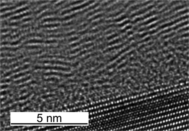
The structure of the BN EE-ALD films was studied with HR-TEM at NIST-Boulder. Figure 9 shows HR-TEM images of a BN film grown at 100 °C with 1000 EE-ALD reaction cycles on a Si(111) substrate. The borazine exposure was 7 × 10⁻² Torr s, and the electron emission current was 100 μA for 240 s. Some of the crystallites have straight, parallel basal planes consistent with hexagonal BN. Other crystallites and interfacial structures display a wavy basal plane characteristic of turbostratic BN.32,33 The crystallites have their basal planes roughly parallel to the substrate surface in both Figure 9a,b. The parallel orientation occurs even though there is a thin amorphous layer with a thickness of ~1 nm between the Si(111) substrate and the BN film.
Figure 9.

HR-TEM images of the BN film grown on Si(111) at 100 °C. (a) BN film displaying basal planes of hexagonal and turbostratic BN approximately parallel to the substrate surface. (b) Interface of the BN film with the Si(111) substrate showing an amorphous BN layer with thickness of ~1 nm.
Previous BN films grown using plasma-enhanced CVD techniques and physical vapor deposition techniques have observed turbostratic BN film growth prior to cubic BN film growth.32–35 The turbostratic (002) basal plane was observed to be perpendicular to initial silicon substrates on a thin amorphous BN layer.32,34 In contrast, turbostratic BN with the (002) basal planes parallel to the substrate surface was observed when the BN films were deposited on a diamond (111) substrate.33 These earlier results for BN films deposited on diamond surfaces are similar to those for the BN films deposited on Si(111) shown in Figure 9a,b.
The crystallinity of the BN EE-ALD films was also verified using GIXRD measurements. Figure 10a shows the GIXRD analysis of a BN film grown at 100 °C with 1000 EE-ALD reaction cycles. The borazine exposure was 7 × 10⁻² Torr s, and the electron emission current was 100 μA for 240 s. This film had a thickness of 1170 Å. Growth rates at 100 °C were found to be approximately one-third the growth rate at 27 °C. For reference, Figure 10b shows a hexagonal BN XRD powder pattern.36 Only two diffraction peaks are observed from the BN EE-ALD film in Figure 10a. These diffraction peaks are consistent with the (002) and (004) diffraction peaks in Figure 10b. A small shift to lower 2θ values is observed relative to the hexagonal BN powder pattern. This shift may result from a slight expansion of the BN lattice.
Figure 10.

(a) GIXRD scan of the BN film grown at 100 °C using 1000 cycles at an electron energy of 100 eV and an electron emission current of 100 μA for 240 s. Borazine exposure was 7 × 10⁻² Torr s. (b) Reference XRD powder pattern of hexagonal BN.
Hexagonal BN has lattice constants of a = 2.504 Å and c = 6.658 Å.37 Turbostratic BN is a variant of hexagonal BN, where stacking faults occur by either a random rotation or dislocation. Depending on the amount of turbostratic BN present in the film, the c lattice parameter can range up to 6.86 Å, while no change is observed in the a parameter.37 The small shifts to lower 2Θ values relative to the hexagonal BN powder pattern are consistent with the presence of turbostratic BN. The broadening of diffraction peaks in Figure 10a is consistent with a fine-grained, polycrystalline BN film. Crystalline size was estimated from the width of the diffraction peaks using the Scherrer formula. The estimated crystallite diameters were 1–2 nm.
Micro-Raman spectroscopy was also performed on a BN sample grown at 100 °C with 1000 EE-ALD reaction cycles. This film had a thickness of 1170 Å. A small Raman peak was observed at 1372 cm−1. This Raman peak is consistent with the symmetric in-plane stretching of hexagonal BN at 1370 cm−1.34,38 Additionally, a BN film with a thickness of 900 Å was grown at 27 °C with 2000 EE-ALD cycles and examined using FTIR spectroscopy. A broad peak was observed at 1367 cm−1. In comparison, the IR active peaks for hexagonal BN are found at 1367–1380 cm−1 for the in-plane stretch and 780–790 cm−1 for out-of-plane bending.34,38,39
3.5. Proposed Growth Mechanism.
In Figures 2–5, the maximum BN growth rates are 3.0–3.2 Å/cycle. This GPC is roughly consistent with the 3.3 Å interlayer spacing of hexagonal BN basal planes along the c-axis. In addition, the deposited BN films have their basal planes aligned approximately parallel to the substrate surface in the HR-TEM measurements. On the basis of these observations, the BN growth mechanism is believed to occur by borazine adsorption with the borazine ring parallel to the surface, as shown in Figure 11.
Figure 11.

Proposed BN growth mechanism during EE-ALD: (a) ESD of hydrogen from borazine and (b) borazine adsorption on the BN surface.
During electron exposure, the hydrogens attached to borazine are believed to be desorbed and highly reactive dangling bonds are left behind on the borazine rings. These dangling bonds can react with neighboring dangling bonds to form BN with the sp2 bond structure, as shown in Figure 11a. After the dangling bonds have reacted to form a BN monolayer, more borazine can be adsorbed on the BN surface, as shown in Figure 11b.
This proposed growth mechanism would lead to BN EE-ALD growth rates of ~3.3 Å/cycle. The orientation of the BN basal planes with the sp2 bond structure would be parallel to the initial substrate. The self-limiting BN EE-ALD growth rate at ~3.0 Å/cycle versus borazine exposure in Figure 3 also argues that the adsorption of a secondary borazine layer or a borazine multilayer on the unreacted, adsorbed borazine layer is unfavorable at room temperature. The absence of a borazine multilayer is consistent with previous temperature-programmed desorption studies where the borazine multilayer is observed to desorb at approximately −100 °C.40,41
3.6. Growth on Patterned Substrates.
EE-ALD is a line-of-sight technique that could provide area-selective deposition because of the directionality of the electron flux on the surface. For an electron beam normal to the substrate, the electron flux is highest on horizontal surfaces and lowest on vertical surfaces that are parallel to the direction of the electron flux. Consequently, EE-ALD should produce deposition preferentially on horizontal surfaces and little deposition on vertical surfaces. This area-selective deposition could lead to the bottom-up filling of high aspect ratio vias or trenches.
BN EE-ALD was employed to coat trench structures with aspect ratios of ~10:1 provided by Applied Materials. Figure 12a displays a STEM image after BN EE-ALD on the trench structure. The BN EE-ALD film was grown at 27 °C with 1000 EE-ALD reaction cycles using an electron energy of 400 eV. The borazine exposure was 7 × 10⁻² Torr s, and the electron emission current was 100 μA for 240 s. The electron flux was close to normal to the substrate and parallel to the axis of the trench structures. However, the alignment of the electron flux with the substrate normal was only visual, and the misalignment could be as much as ±5°. In addition, the electron beam from the electron gun has some divergence. The electron beam has a diameter of ~10 mm at the substrate. Simulations indicate that the divergence of the electron beam is ±10° off-normal at ±5 mm from the center of the electron beam.
Figure 12.

BN EE-ALD on the trenched substrate. The film was grown at 27 °C with 1000 EE-ALD reaction cycles using an electron energy of 400 eV with an electron emission current of 100 μA for 240 s. Borazine exposure was 7 × 10⁻² Torr s. (a) STEM image shows the BN film deposited on top of the trench structure with little film deposition on trench sidewalls. (b) STEM/EELS for B, N, Si, and O on the trench sidewalls and a false-colored, combined elemental map on the far right.
Figure 12a shows a BN film with a thickness of ~50 nm on the SiNx layer on top of the trenched substrate. The BN film is the very light gray layer on the top horizontal surface of Figure 12a. In comparison, there is only a very thin BN film on the sides of the trench. The BN film has achieved area-selective deposition on the top of the trenched structure. If the electron flux is aligned normal to the substrate, then the BN film thickness at the bottom of the trench should be equivalent to the BN film thickness on the top of the trenched substrate. The thinner than expected BN film at the bottom of the trench may result from the misalignment of the electron flux with respect to the substrate normal. For a ~10:1 aspect ratio, electrons that enter the center of the trench can reach the bottom of the trench only if they have an incoming angle of <±3° from the normal to the substrate.
STEM/EELS measurements have also examined the elemental composition of the BN film on the sides of the same trenches in Figure 12a. The individual panels in Figure 12b show results for B, N, Si, and O from left to right. The image on the far right in Figure 12b shows a color composite of all the elements. B is red, N is lavender, and BN appears as a pink-purple color. A thick BN EE-ALD film is clearly observed on the top horizontal surface by the STEM/EELS measurements. Much less BN is measured on the more vertical sides of the trench.
The BN film thickness on the trench sidewalls is attributed to β, the angle of the incoming electron beam relative to the surface normal of the trench sidewall. The electron flux on the trench sidewall will vary with cos β. In addition, there could also be a misalignment angle, Δ, of the electron flux relative to the surface normal of the substrate. The various BN film thicknesses on the trench sidewalls were measured for the different β angles that vary from approximately 75°–85° in Figure 12. A good fit of these BN film thicknesses and the BN film thickness on top of the substrate is obtained by assuming that the BN film thickness is proportional to [1–exp(–cos[β + Δ]t/τ], where Δ = 3.6°. The misalignment angle is within the range of ±5° expected for the visual alignment of the electron beam. The misalignment angle is also consistent with the smaller BN film thickness observed at the bottom of the trench.
Deposition is needed to fill vias from the bottom to the top without depositing on sidewalls to avoid pinch-off. Pinch-off occurs when film deposition on sidewalls accumulates and closes the opening through the via. Pinch-off causes voids inside the via and degrades device performance. On the basis of these results for patterned substrates, preferential bottom-up filling could be observed on vertical trench structures using EE-ALD. Implementing bottom-up filling using EE-ALD requires the electrons to be incident at the bottom of the trench structure. For ~10:1 aspect ratios, the electron flux must be aligned with the substrate normal with a maximum divergence of <3°. This electron flux alignment may require a more collimated electron beam or sample biasing.
4. CONCLUSIONS
BN films were grown using EE-ALD techniques with sequential exposures of borazine and low-energy electrons at 27 and 100 °C. The BN film growth is believed to result from hydrogen ESD from borazine that results in dangling bond production. The highly reactive dangling bonds can then react with each other to form a hexagonal BN layer. Self-limiting BN EE-ALD growth behavior was observed with respect to borazine exposure, electron exposure time, and electron emission current. In addition, the BN film thickness increased linearly with BN EE-ALD cycles for various reaction conditions. Maximum BN growth rates of 3.2 Å/cycle were observed at electron energies of 80–160 eV. An average hydrogen ESD cross section of σ = 4.2 × 10⁻¹⁷ cm2 was obtained from fitting the BN GPC versus electron exposure time, fitting the BN GPC versus electron emission current, and fitting the spatial profile of the BN film thickness assuming a Gaussian electron beam profile.
The BN films deposited at 100 °C were observed to be fine-grained, polycrystalline hexagonal BN by GIXRD and Raman and FTIR spectroscopies. HR-TEM analysis was consistent with hexagonal and turbostratic BN with the basal planes approximately parallel to the substrate surface. The BN crystallite size was estimated to be 1–2 nm in diameter by GIXRD. The film composition from XPS was slightly boron-rich (B/N, 1.1:1) with ~2 at. % carbon and oxygen contamination. Additionally, these BN films were stable in atmosphere and formed a self-passivating oxide layer.
The BN film growth was very conformal across the ~1 cm2 growth area defined by the electron beam. Additionally, the BN film growth on trenched structures displayed preferential growth on the top horizontal surface of the substrate. The directionality of the electron flux leads to area-selective deposition. These results suggest that EE-ALD could be used for bottom-up filling of trenches and vias during semiconductor processing. In addition, BN EE-ALD at room temperature offers possible avenues for BN deposition on thermally sensitive substrates.
ACKNOWLEDGMENTS
This work was supported by Defense Advanced Research Projects Agency (DARPA) under Grant W911NF-13-1-0041. The authors thank Tyler McQuade and Anne Fischer from DARPA for their support and helpful comments. The authors also acknowledge Kenneth Smith and Don David from the University of Colorado Integrated Instrument Development Facility for their help with the experimental apparatus and computer interfacing. In addition, the authors acknowledge Mark Saly from Applied Materials for providing the patterned substrates and Kathryn Wahl from the Naval Research Laboratory for confirming the GIXRD analysis. The authors also thank Andrew Tomaschke from the University of Colorado at Boulder for the Raman measurements, Greg Haugstad from the University of Minnesota Characterization Facility for the FRES studies, and Russell Perkins from the University of Colorado at Boulder for the FTIR analysis.
Footnotes
The authors declare no competing financial interest.
REFERENCES
- (1).Huth M; Porrati F; Schwalb C; Winhold M; Sachser R; Dukic M; Adams J; Fantner G Focused Electron Beam Induced Deposition: A Perspective. Beilstein J. Nanotechnol 2012, 3, 597–619. [DOI] [PMC free article] [PubMed] [Google Scholar]
- (2).van Dorp WF; Hagen CW A Critical Literature Review of Focused Electron Beam Induced Deposition. J. Appl. Phys 2008, 104, 081301. [Google Scholar]
- (3).Böhler E; Warneke J; Swiderek P Control of Chemical Reactions and Synthesis by Low-energy Electrons. Chem. Soc. Rev 2013, 42, 9219–9231. [DOI] [PubMed] [Google Scholar]
- (4).Thorman RM; Kumar TP,R; Fairbrother DH; Ingólfsson O The Role of Low-energy Electrons in Focused Electron Beam Induced Deposition: Four Case Studies of Representative Precursors. Beilstein J. Nanotechnol 2015, 6, 1904–1926. [DOI] [PMC free article] [PubMed] [Google Scholar]
- (5).Lafosse A; Bertin M; Cáceres D; Jäggle C; Swiderek P; Pliszka D; Azria R Electron Induced Functionalization of Diamond by Small Organic Groups. Eur. Phys. J. D 2005, 35, 363–366. [Google Scholar]
- (6).Sprenger JK; Cavanagh AS; Sun H; Wahl KJ; Roshko A; George SM Electron Enhanced Growth of Crystalline Gallium Nitride Thin Films at Room Temperature and 100 °C Using Sequential Surface Reactions. Chem. Mater 2016, 28, 5282–5294. [DOI] [PMC free article] [PubMed] [Google Scholar]
- (7).George SM Atomic Layer Deposition: An Overview. Chem. Rev 2010, 110, 111–131. [DOI] [PubMed] [Google Scholar]
- (8).Sprenger JK; Sun H; Cavanagh AS; George SM Electron-Enhanced Atomic Layer Deposition of Silicon Thin Films at Room Temperature. J. Vac. Sci. Technol., A 2018, 36, 01A118. [PMC free article] [PubMed] [Google Scholar]
- (9).Dean CR; Young AF; Meric I; Lee C; Wang L; Sorgenfrei S; Watanabe K; Taniguchi T; Kim P; Shepard KL; Hone J Boron Nitride Substrates for High-Quality Graphene Electronics. Nat. Nanotechnol 2010, 5, 722–726. [DOI] [PubMed] [Google Scholar]
- (10).Zhang M; Zhu Y; Wang X; Feng Q; Qiao S; Wen W; Chen Y; Cui M; Zhang J; Cai C Controlled Synthesis of ZrS2 Monlayer and Few Layers on Hexagonal Boron Nitride. J. Am. Chem. Soc 2015, 137, 7051–7054. [DOI] [PubMed] [Google Scholar]
- (11).Kumar NA; Dar MA; Gul R; Baek J-B Graphene and Molybdenum Disulfide Hybrids: Synthesis and Applications. Mater. Today 2015, 18, 286–298. [Google Scholar]
- (12).Roy T; Tosun M; Kang JS; Sachid AB; Desai SB; Hettick M; Hu CC; Javey A Field-Efect Transistors Built from All Two-Dimensional Material Components. ACS Nano 2014, 8, 6259–6264. [DOI] [PubMed] [Google Scholar]
- (13).Britnell L; Gorbachev RV; Jalil R; Belle BD; Schedin F; Mishchenko A; Georgiou T; Katsnelson MI; Eaves L; Morozov SV; Peres NMR; Leist J; Geim AK; Novoselov KS; Ponomarenko LA Field-Effect Tunneling Transistor Based on Vertical Graphene Heterostructures. Science 2012, 335, 947–950. [DOI] [PubMed] [Google Scholar]
- (14).Khan MH; Casillas G; Mitchell DRG; Liu HK; Jiang L; Huang Z Carbon- and Crack-Free Growth of Hexagonal Boron Nitride Nanosheets and Their Uncommon Stacking Order. Nanoscale 2016, 8, 15926–15933. [DOI] [PubMed] [Google Scholar]
- (15).Li J-S; Zhang C-R; Li B; Cao F; Wang S-Q Boron Nitride Coatings by Chemical Vapor Deposition from Borazine. Surf. Coat. Technol 2011, 205, 3736–3741. [Google Scholar]
- (16).Shi Y; Hamsen C; Jia X; Kim KK; Reina A; Hofmann M; Hsu AL; Zhang K; Li H; Juang Z-Y; Dresselhaus MS; Li L-J; Kong J Synthesis of Few-Layer Hexagonal Boron Nitride Thin Film by Chemical Vapor Deposition. Nano Lett. 2010, 10, 4134–4139. [DOI] [PubMed] [Google Scholar]
- (17).Ferguson JD; Weimer AW; George SM Atomic Layer Deposition of Boron Nitride using Sequential Exposures of BCl3 and NH3. Thin Solid Films 2002, 413, 16–25. [Google Scholar]
- (18).Driver MS; Beatty JD; Olanipekun O; Reid K; Rath A; Voyles PM; Kelber JA Atomic Layer Epitaxy of h-BN(0001) Multilayers on Co(0001) and Molecular Beam Epitaxy Growth of Graphene on h-BN(0001)/Co(0001). Langmuir 2016, 32, 2601–2607. [DOI] [PubMed] [Google Scholar]
- (19).Jones J; Beauclair B; Olanipekun O; Lightbourne S; Zhang M; Pollok B; Pilli A; Kelber J Atomic Layer Deposition of h-BN(0001) on RuO2(110)/Ru(0001). J. Vac. Sci. Technol., A 2017, 35, 01B139. [Google Scholar]
- (20).Mårlid B; Ottosson M; Pettersson U; Larsson K; Carlsson J-O Atomic Layer Deposition of BN Thin Films. Thin Solid Films 2002, 402, 167–171. [Google Scholar]
- (21).Hwang B; Kwon J; Lee M; Lim SJ; Jeon S; Kim S; Ham U; Song YJ; Kuk Y Electron-beam Assisted Growth of Hexagonal Boron-nitride Layer. Curr. Appl. Phys 2013, 13, 1365–1369. [Google Scholar]
- (22).Fuse T; Fujino T; Ryu J-T; Katayama M; Oura K Electron-Stimulated Desorption of Hydrogen from H/Si(001)-1×1 Surface Studied by Time-of-Flight Elastic Recoil Detection Analysis. Surf. Sci 1999, 420, 81–86. [Google Scholar]
- (23).Matsunami N; Hasebe Y; Itoh N Determination of the Absolute Cross Scetion of Electron-Stimulated-Desorption of Deuterium from Si (111). Surf. Sci 1987, 192, 27–35. [Google Scholar]
- (24).Antoniewicz PR Model for Electron-Stimulated and Photon-Stimulated Desorption. Phys. Rev. B: Condens. Matter Mater. Phys 1980, 21, 3811–3815. [Google Scholar]
- (25).Feibelman PJ; Knotek ML Reinterpretation of Electron-Stimulated Desorption Data from Chemisorption Systems. Phys. Rev. B: Condens. Matter Mater. Phys 1978, 18, 6531–6539. [Google Scholar]
- (26).Menzel D; Gomer R Desoption from Metal Surfaces by Low-Energy Electrons. J. Chem. Phys 1964, 41, 3311–3328. [Google Scholar]
- (27).Redhead PA Interactions of Slow Electrons with Chemisorbed Oxygen. Can. J. Phys 1964, 42, 886–905. [Google Scholar]
- (28).Commercial equipment, instruments, or materials are identified only in order to adequately specify certain procedures. In no case does such identification imply recommendation or endorsement by the National Institute of Standards and Technology, nor does it imply that the products identified are necessarily the best available for the purpose. [Google Scholar]
- (29).Li J-S; Zhang C-R; Li B; Cao F; Wang S-Q An Improved Synthesis of Borazine with Aluminum Chloride as Catalyst. Eur. J. Inorg. Chem 2010, 2010, 1763–1766. [Google Scholar]
- (30).Goeden C; Dollinger G Electron Stimulated Desorption of Diamond (100) as a Negative Hydrogen Source. Appl. Surf. Sci 1999, 147, 107–113. [Google Scholar]
- (31).Madey TE; Yates JT Electron-Stimulated Desorption as a Tool for Studies of Chemisorption: A Review. J. Vac. Sci. Technol 1971, 8, 525–555. [Google Scholar]
- (32).Yang HS; Iwamoto C; Yoshida T Nanostructures of the Turbostratic BN Transition Layer in Cubic BN Thin Films Deposited by Low-pressure Inductively Coupled Plasma-enhanced Chemical Vapor Deposition. J. Appl. Phys 2002, 91, 6695–6699. [Google Scholar]
- (33).Zhang WJ; Meng XM; Chan CY; Chan KM; Wu Y; Bello I; Lee ST Interfacial Study of Cubic Boron Nitride Films Deposited on Diamond. J. Phys. Chem. B 2005, 109, 16005–16010. [DOI] [PubMed] [Google Scholar]
- (34).Zhang WJ; Chong YM; Bello I; Lee ST Nucleation, Growth and Characterization of Cubic Boron Nitride (cBN) Films. J. Phys. D: Appl. Phys 2007, 40, 6159–6174. [Google Scholar]
- (35).Hofsäss H; Eyhusen S; Ronning C On the Mechanisms of Cubic Boron Nitride Film Growth. Diamond Relat. Mater 2004, 13, 1103–1110. [Google Scholar]
- (36).Brager A An X-ray Examination of the Structure of Boron Nitride. Acta Physicochim. URSS 1937, 7, 699–706. [Google Scholar]
- (37).Kurdyumov AV; Solozhenko VL; Zelyavski WB Lattice Parameters of Boron Nitride Polymorphous Modifications as a Function of Their Crystal-Structure Perfection. J. Appl. Crystallogr 1995, 28, 540–545. [Google Scholar]
- (38).Geick R; Perry CH; Rupprech G Normal Modes in Hexagonal Boron Nitride. Phys. Rev 1966, 146, 543–547. [Google Scholar]
- (39).Nocua JE; Piazza F; Weiner BR; Morell G High-Yield Synthesis of Stoichiometric Boron Nitride Nanostructures. J. Nano-mater 2009, 2009, 1–6. [Google Scholar]
- (40).He JW; Goodman DW Interaction of Borazine with a Re(0001) Surface, Studied by LEED, TDS, AES and ELS. Surf. Sci 1990, 232, 138–148. [Google Scholar]
- (41).Paffett MT; Simonson RJ; Papin P; Paine RT Borazine Adsorption and Decomposition at Pt(111) and Ru(001) Surfaces. Surf. Sci 1990, 232, 286–296. [Google Scholar]