Abstract
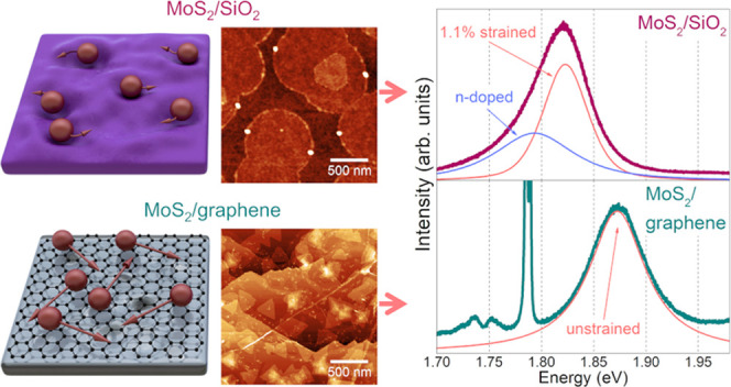
In this work, we report the impact of substrate type on the morphological and structural properties of molybdenum disulfide (MoS2) grown by chemical vapor deposition (CVD). MoS2 synthesized on a three-dimensional (3D) substrate, that is, SiO2, in response to the change of the thermodynamic conditions yielded different grain morphologies, including triangles, truncated triangles, and circles. Simultaneously, MoS2 on graphene is highly immune to the modifications of the growth conditions, forming triangular crystals only. We explain the differences between MoS2 on SiO2 and graphene by the different surface diffusion mechanisms, namely, hopping and gas-molecule-collision-like mechanisms, respectively. As a result, we observe the formation of thermodynamically favorable nuclei shapes on graphene, while on SiO2, a full spectrum of domain shapes can be achieved. Additionally, graphene withstands the growth process well, with only slight changes in strain and doping. Furthermore, by the application of graphene as a growth substrate, we realize van der Waals epitaxy and achieve strain-free growth, as suggested by the photoluminescence (PL) studies. We indicate that PL, contrary to Raman spectroscopy, enables us to arbitrarily determine the strain levels in MoS2.
Keywords: MoS2, graphene, CVD, van der Waals heterostructures, photoluminescence, surface diffusion
Introduction
Two-dimensional (2D) semiconductors are currently of interest to the research community as they are foreseen to be important building blocks for beyond-silicon electronics. MoS2, a transition-metal dichalcogenide (TMDC), is the most researched representative of 2D semiconductors due to the presence of a direct band gap, which changes to indirect with an increasing number of layers,1 and due to widespread material availability. It can be used in a variety of applications, including transparent photodetectors,2 field-effect transistors,3 photoresponsive memory devices,4 and quantum well light-emitting diodes.5 There are two main methods to obtain MoS2 monolayers: mechanical exfoliation6 and chemical vapor deposition (CVD).7 Mechanical exfoliation, despite yielding high-quality flakes, is not scalable and repeatable, whereas CVD is much more controllable and is suitable for industrial-scale production. There are numerous modifications of CVD; however, in the context of MoS2 growth, only two methods are relevant, namely, metal–organic chemical vapor deposition (MOCVD)8 and thermal vapor deposition (TVD).9 While MOCVD is an industrially proven technique to produce high-quality crystals,10 TVD is a perfect platform for proof-of-concept studies at the laboratory scales. Additionally, the knowledge gained during TVD growth can be directly transferred to industrial-scale reactors, as in the case of graphene.11
One of the most important variables in the growth of MoS2 is the substrate. There are several suitable platforms for MoS2 growth, with SiO2 and sapphire being the most widely used due to their affordability.12 Alternatively, graphene can also be used as a growth platform for MoS2.3 Additionally, the use of a 2D material as a substrate for the growth of other 2D materials results in the creation of van der Waals (vdW) heterostructures.13 These heterostructures are superior to the classical heterostructures as the epitaxial layer is bound only by weak van der Waals forces, so extreme lattice mismatches can be accommodated (e.g., graphene and MoS2 have mismatch equal to 28%).14 Interestingly, despite the weak interaction between materials, the grown material follows the crystallographic orientation of the substrate, which should result in perfect alignment and strain-free growth.15
Recently, research interest in MoS2–graphene vdW heterostructures is increasing; however, the majority of the articles are presenting the structures created with at least one transfer step.16−19 Still, several scientific papers are reporting all-CVD growth of MoS2/graphene vdW sandwich,20−22 suitable for the industrial implementation. It has to be noted, however, that most of these stacks are grown on a metallic substrate, preventing full exploitation of the potential of graphene-based heterostructures. There are only a handful of reports showing van der Waals epitaxy of MoS2 on graphene synthesized on insulating substrates.23−27 These works are presenting the fundamental research on these vdW heterostructures, focused mainly on the electronic behavior of the materials. For instance, the application of semi-freestanding epitaxial graphene on SiC as a growth platform allowed the electronic structure of the MoS2/graphene heterostructure to be revealed.25 Also, the structural properties have been characterized, and it was proved that MoS2 is commensurate to epitaxial graphene, growing with two preferential domain orientations.26 While these investigations are valuable, still more research is needed to understand the CVD-grown MoS2/graphene system. A convincing explanation of how the epitaxial graphene is influencing the growth of MoS2 is still lacking, especially in the context of arbitrary substrates like SiO2 or sapphire. Also, a more thorough analysis of the impact of the MoS2 growth on graphene quality is yet to be presented. Moreover, the strain state of MoS2 on graphene is still under discussion, and various works are presenting different, contradictory conclusions.18,26
In this article, we present a direct comparison between MoS2 grown on graphene, SiO2, and sapphire, and we explain how the obtained layers are affected by the growth platform. In particular, we show that the morphology of MoS2 grains on graphene is unusually stable and practically unchanged by the modification of the growth conditions. Furthermore, we present a viable kinetics-based explanation for the observed effects. In addition, for the first time, we present a method to obtain circular MoS2 domains on SiO2 and sapphire, complemented by the possible growth model. The results are supported by thorough Raman and photoluminescence (PL) analyses, showing how graphene is affected by the growth. We also indicate PL as a method that enables us to arbitrarily determine the strain levels in MoS2, and we show that MoS2 grown on graphene follows van der Waals epitaxy, resulting in unstrained growth.
Experimental Section
CVD Growth of Graphene and Substrate Preparation
The detailed graphene growth procedure was presented elsewhere.11 Polycrystalline graphene was grown in an experimental AIXTRON reactor. As a substrate, 2-in. single-side-polished c-plane sapphire wafers were used. The process was carried out for 4 min at 1560 °C, and methane was used as a carbon precursor.
For the MoS2 growth, we used three types of substrates: SiO2/Si (n-type, 285 nm thick thermal oxide), sapphire (c-plane), and graphene/sapphire. SiO2, graphene, and sapphire were manually cleaved into 8 × 8 mm2 pieces. Except for argon flushing, no additional cleaning procedure was applied for all substrates.
CVD Growth of MoS2
CVD growth of MoS2 was carried out in a tube furnace (Figure 1). As a work tube, we used a 1200 mm 2-in. quartz tube. To limit parasitic reactions, we used two 1-in. quartz tubes, and in each, we placed one precursor. As precursors, we used MoO3 (Alfa Aesar, 99.95%) and sublimated sulfur (Chempur, pure p.a.), and Ar served as a carrier gas. Metallic Mo tiles (99%) with a naturally formed oxide layer were used as an additional source of molybdenum oxide. The substrates were placed on a quartz rod, approximately 8 mm above the bottom of the work tube, and 10 and 40 cm from Mo and S precursors, respectively, to increase the uniformity across samples. An additional custom-made heater was added to the system to enable better control of the sulfur temperature. To ensure the process repeatability, the substrates, precursors, quartz elements, and sulfur heater between the growth runs were placed in the same positions with an accuracy of ±1 mm. All of the measurements were performed in the centers on the samples to reduce the effects of the disturbed gas flow at the edges of the substrates. The standard growth parameters are presented in Table 1.
Figure 1.
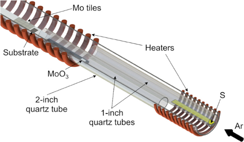
Scheme of tube furnace used for the growth of MoS2.
Table 1. Standard Growth Run Parameters.
| parameter | value |
|---|---|
| substrate temperature | 770 °C |
| MoO3 temperature | 687 ± 15 °C |
| S temperature | 115 °C |
| weight of MoO3 | 50 mg |
| weight of S | 125 mg |
| evaporation area of MoO3 | 0.5 cm2 |
| evaporation area of S | 10 cm2 |
| pressure | 930 mbar |
| Ar flow | 100 sccm |
| growth time | 15 min |
Characterization
To determine the morphology of the obtained MoS2 layers, we used a Bruker Dimension Icon atomic force microscope (AFM). The topography of samples was measured in tapping and PeakForce modes using standard (tip radius ∼10 nm) and supersharp (tip radius ∼1 nm) probes, respectively. Scanning electron microscopy (SEM) images were taken in RAITH eLINE plus electron-beam lithography SEM with an in-lens detector.
The as-grown samples were characterized by means of Raman spectroscopy and photoluminescence. For this purpose, we used a Renishaw inVia Qontor Raman spectroscope in a backscattering configuration equipped with xyz stage with a resolution of 100 nm. All measurements were done with 532 nm laser, 50× objective, 1800 lines/mm grating, and 8 mW laser power. To exclude laser-induced effects, we minimized laser power density on the sample using a relatively large laser beam spot size approximately 4 μm in diameter. Circularly polarized light was used to eliminate any symmetry-based phenomena. A detailed explanation and discussion about this measurement condition can be found in our previous work.28 Statistical measurements were obtained in the form of square Raman maps over an area of 40 × 40 μm2 with 196 points distributed at 3 μm steps in both x and y directions.
Results and Discussion
Direct Comparison between MoS2 Grown on SiO2, Sapphire, and Graphene
The initial investigation was focused on achieving individual MoS2 grains on three substrates to compare their morphology. AFM images of MoS2 grown on SiO2, sapphire, and graphene are shown in Figure 2, accompanied by height profiles. The height profiles on each substrate show MoS2 layers approximately 0.7 nm thick, proving the monolayer nature of these as-grown nuclei. The MoS2 grain morphology, however, is different on each substrate. MoS2 on SiO2 and sapphire tends to form circular domains, whereas on graphene, these grains are triangular. The largest domains and smallest nucleation density were achieved on SiO2.
Figure 2.
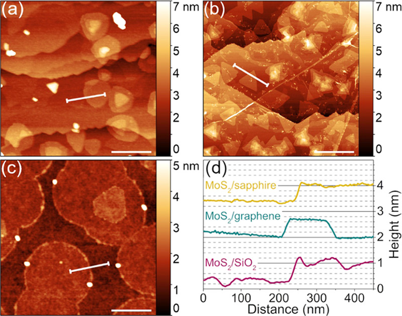
AFM images of MoS2 grown on: (a) sapphire, (b) graphene, (c) SiO2, and (d) corresponding height profiles. The samples have been grown with standard growth conditions. The scale bars are 500 nm.
To confirm the chemical composition and presence of MoS2 on the substrates, we conducted simple Raman characterization, shown in Figure 3. MoS2 E2g and A1g peaks are present on all three samples, and the peak separations are small, that is, 19, 21.3, and 22.1 cm–1 for SiO2, graphene, and sapphire, respectively, indicating the presence of monolayer MoS2. Additionally, on graphene and sapphire substrates, the A1g peak of sapphire can also be noted. The MoS2 peaks are positioned differently on each substrate, which will be discussed later.
Figure 3.
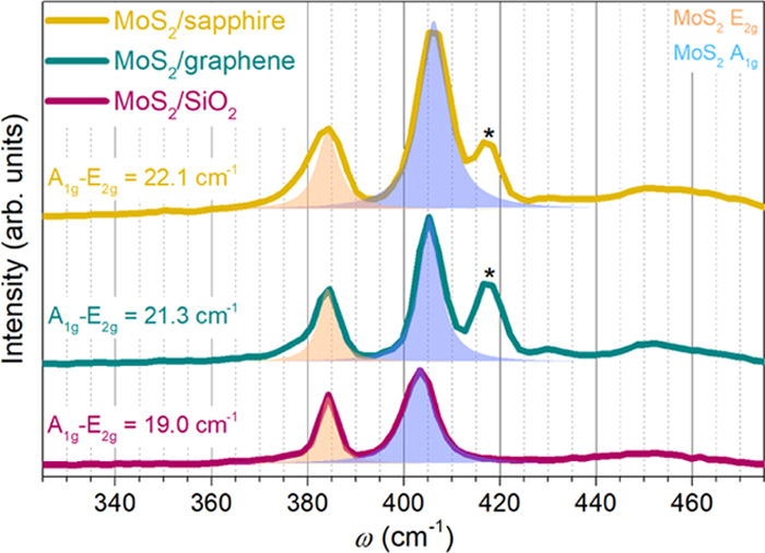
Raman spectra of discrete MoS2 islands on three substrates. Raman spectra are normalized to MoS2 E2g peaks. The sapphire A1g peaks were marked with asterisks.
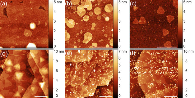
After establishing the standard growth parameters, we focused on the detailed investigations of the MoS2 synthesis on graphene. For a reference substrate, we chose only SiO2, which was then always inserted into the reactor chamber alongside graphene. As we were modifying several variables, that is, substrate temperature (770–900 °C), the flux of sulfur (modified by its temperature in the range of 115–180 °C), precursor evaporation area and weight, the distance between the precursors, and growth time (15–60 min), we observed only minor changes in MoS2 morphology on graphene samples, namely, slight variations in grain size and nucleation density (Figure 4d–f). On the contrary, the morphology of MoS2 grains on SiO2 was much more diverse, changing from higher coverage to circles with a higher number of adlayers and to truncated triangles (Figure 4a–c).
Figure 4.
MoS2 grain morphologies observed in modified growth conditions on SiO2 (a–c) (scale bars 2 μm) and on graphene (d–f) (scale bars 500 nm). The growth conditions were modified as follows: (a, d): the growth time was increased to 60 min; (b, e) the substrate temperature was increased to 900 °C; (c, f) the S flux was increased approximately 20-fold, and it was achieved by changing S weight to 1000 mg and increasing the S temperature to 180 °C.
Chemistry of CVD Synthesis of MoS2
The unusual stability of MoS2 growth on graphene needs more attention. Before we explain the observed differences of MoS2 morphology on different substrates, it is necessary to introduce several theoretical aspects of CVD growth. First of all, it has to be determined how the MoS2 synthesis occurs. The most accepted route for the formation of MoS2 from MoO3 and S is as follows29
| 1 |
In fact, the synthesis of MoS2 during CVD growth does not involve single MoO3 and S species. Instead of atomic sulfur, sulfur molecules, Sn, with n between 2 and 8, are present in the gaseous form, and S8 is the most abundant.30 Similarly, also no single MoO3 molecule reacts in the vapor, but rather MonO3n polymeric species with 3 ≤ n ≤ 5, and Mo3O9 constitutes 70% of the vapor.31 The more adequate chemical reaction, therefore, should involve S8 and Mo3O9 rather than atomic S and MoO3. Currently, no reports are discussing whether MoS2 in the gaseous form is a single molecule or a cluster. Still, as the structure of Mo3O932 is similar to the structure of MoS2, Mo3S6 clusters might be present in the vapor.
There are two hypotheses discussing where the reduction of Mo-containing species occurs: in the first, the reaction is occurring purely in the gas phase,33 while the second advocates that the partially reduced MoO3–x is adsorbed on the substrate and is further reduced by sulfur on-site.29 The driving force for the CVD growth is the local supersaturation of a metastable phase at a surface. The three chemical species present during the growth have distinctly different vapor pressures, indicating the different abilities to form supersaturated medium. The equilibrium vapor pressures of MoO3 and S at the standard growth temperature are easy to compute and are equal to 4.2 mbar34 and 21.4 bar,35 respectively.
However, there are no reports showing the value of MoS2 vapor pressure at high temperatures. Extrapolating the evaporation rate of MoS2 obtained by Bisson to 770 °C,36 the calculated value of MoS2 vapor pressure is approximately 0.1 mbar, which is significantly lower than the vapor pressure of MoO3 and S. Since the growth occurs and MoS2 has the lowest vapor pressure among the three compounds, it is likely that the growth is driven by the adsorption and coalescence of gaseous MoS2 molecules synthesized in the vapor phase rather than on-site reduction of MoO3. Furthermore, if MoO3 and S adsorb on the substrate, their presence should be visible in Raman spectroscopy measurements. It is not the case as except MoS2 and substrate peaks, no more chemical compounds are present.
Surface Kinetics and Thermodynamics of CVD Growth
Since growth conditions were the same for all substrates, the apparent differences in MoS2 layer properties originate solely from the growth platforms. Indeed, one can enumerate several differences between the three substrates, including crystallinity or surface energy. However, the ability of a substrate to create bonds with the synthesized layer is arguably the most important feature in the context of CVD growth of 2D materials. Carbon atoms forming the graphene layer cannot create any new chemical bonds, which is also characteristic of any layered 2D material, including MoS2. Therefore, only very weak interactions between adsorbed species and graphene can be expected, which is the main prerequisite for the van der Waals epitaxy.37,38
The ability of the substrate to create bonds significantly influences the dynamics of adsorbates at the substrate surface, especially the surface diffusion mechanism. In typical three-dimensional (3D) materials, that is, with unsaturated bonds on the surface, including SiO2 or sapphire, the mechanism of surface diffusion is described by a hopping model in which adsorbed species are localized at high-energy-binding sites on the surface,39 for example, active hydroxyl groups on SiO240 (Figure 5). The movement of the species is allowed only between these binding sites. These hydroxyl groups can also become nucleation sites for MoS2 growth as the predicted activation energies of R3–Si–O–MoS2 from R3–Si–OH are similar to the thermal energy of gas molecules at the growth temperature, that is, 156 and 135 meV, respectively.40
Figure 5.
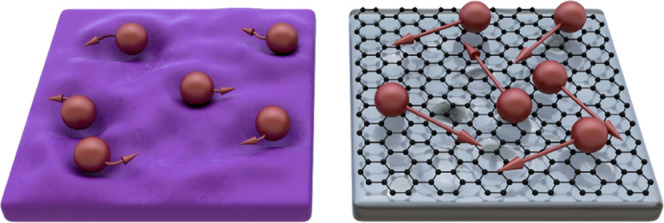
Schematic representations of the movement of the adsorbed MoS2 species (red balls) on SiO2 (left) and graphene/sapphire (right). The valleys on the SiO2 surface represent high-energy binding sites. The schematic is not to scale.
It has to be noted, however, that the hopping mechanism is not valid for some materials. There are studies of gas movement on weakly interacting surfaces, for example, Xe, Kr, CH4, or NO on graphite,41 that showed the surface diffusion should be rather described as a so-called mobile diffusion.42 In this mechanism, the gas molecules are forming a 2D gas directly above the surface and are no longer bound to the high-energy sites, moving virtually unrestricted over the substrate surface. Importantly, strikingly similar behavior has been theoretically predicted for graphene, on which the surface diffusion is governed by a gas-molecule-collision-like mechanism.43
It is commonly known that for the hopping mechanism, the surface mean free path44 and the residence time44,45 of adsorbed molecules are decreasing with an increase of temperature. Currently, there are no studies showing the impact of elevated temperatures on the mean free path of adsorbed gases on graphene. However, in the ideal gas case, the energy of molecules as well as the distance traveled are increasing at higher temperatures. As the surface diffusion on graphene is similar to the ideal gas, it is likely that the mean free path will also increase. On the other hand, in the ideal gas approximation, the residence time is shorter at elevated temperatures, similarly to the hopping mechanism.
Besides surface kinetics, also the ratio of available chemical species as a part of the growth thermodynamics has to be discussed to describe a wide range of MoS2 morphologies. As theoretically predicted by Cao et al.,46 a S-rich environment drives the growth of the triangular domains. When decreasing the amount of available sulfur, the domains are becoming truncated triangles and hexagons. In a Mo-rich environment, the domains should take the form of dodecagons. Interestingly, almost every predicted domain shape has been obtained experimentally,47,48 except dodecagons, which we will discuss later.
Explanation of the Observed Differences in MoS2 Grain Morphology
We suggest that the observed differences in the various substrates can be explained in terms of the different surface diffusion mechanisms. On graphene, the surface diffusion manifests as the gas-molecule-collision-like mechanism (shown schematically in Figure 5), and the adsorbed MoS2 can travel at significant distances to find the energetically favorable sites. As a result, the kinetics is not limiting the growth, and the domains tend to form thermodynamically favorable shapes. Furthermore, one can observe second-layer domains on SiO2 in Figures 2c and 4b. Contrary to the first MoS2 layer, the adlayers are angular, taking the form of triangles and truncated triangles. In this case, the first layer serves as a van der Waals substrate; hence, the surface diffusion mechanism should be similar to the case of graphene. As a result, the growth of the first MoS2 layer is limited by the SiO2, while the growth of the second MoS2 layer is analogous to the growth of MoS2 on graphene.
The explanation for the formation of circular domains on SiO2 should be based both on the growth kinetics and thermodynamics. Instead of theoretically predicted dodecagons, it was more favorable for MoS2 domains to form circles. The typical growth run was conducted at a very low sulfur flux, which is the limiting growth process factor. Moreover, carrier gas flow and growth temperature were also relatively low. SiO2 and sapphire have unsaturated bonds, and the surface diffusion is moderated by hopping mechanism, which results in a short surface mean free path of adsorbed MoS2 at growth temperatures. Hence, the adsorbed MoS2 species are binding to the existing nuclei at random sites rather than energetically favorable ones, as a result forming circles. Still, with an increase of S flux, resulting in the change of the thermodynamic conditions, it is possible to obtain angular shapes at different growth temperatures, confirming the limiting nature of the Mo/S ratio.
Another hypothesis, assuming that the circular domains are amorphous, should not be treated as valid as it can be seen in Figure 4b that different adlayer nuclei grown on individual first-layer domains are rotated only at two preferential angles, that is, 0 and 60°. If the hypothesis of amorphous islands would be valid, the domains would have been rotated randomly as the first layer on SiO2 in Figure 4c. Interestingly, Zhang et al.49 also presented circular domains very similar to our results, and transmission electron microscopy (TEM) and selected area electron diffraction (SAED) proved the monocrystalline nature of these domains. These observations strongly suggest that the surface diffusion is low enough to allow the formation of circular domains but high enough to allow the adsorbates to rotate, forming a monocrystal. In the case of sapphire, the formation of circles is less pronounced, as on the crystalline substrate, the movement of the adsorbed species is less restricted, leading to the formation of rounded triangles.
We conclude that on SiO2, the surface diffusion realized by a hopping mechanism drives the MoS2 growth, as a result forming a variety of domains, including circles. Simultaneously, MoS2 growth on graphene is probably close to thermodynamic equilibrium due to the gas-molecule-collision-like mechanism, and it can explain the relatively low responsiveness to the change of the growth conditions. Also, we want to note that by using 2D material as a growth platform we only can extend the technological window for MoS2 growth, and for more extreme growth conditions, the growth of angular crystals might not be possible.
Impact of a Continuous MoS2 Layer on Graphene
To thoroughly investigate MoS2 on graphene, we synthesized a continuous layer. It has been achieved by a modification of the thermodynamic conditions, namely, by placing the substrates significantly closer to the precursors. The SEM image of a continuous layer on graphene is presented in Figure 6a. It is possible to see that besides monolayer, also bi- and multilayers have been grown (Figure 6b). Interestingly, these adlayers are forming a network without any particular direction, and it is caused by the fact that MoS2 tends to grow on defects,50 in this case, on graphene wrinkles. For comparison, also the SEM image of a continuous layer on SiO2 is presented in Figure 6c. Several cracks of the layer can be seen, and a notable number of adlayers is visible but still lower than that in the case of graphene.
Figure 6.
SEM micrographs in in-lens contrast of continuous layer of MoS2 on: (a) graphene (scale bar, 10 μm), (b) graphene, with visible bi- and multilayers as black areas (scale bar, 1 μm), and (c) SiO2, with a crack marked with a black arrow (scale bar, 10 μm).
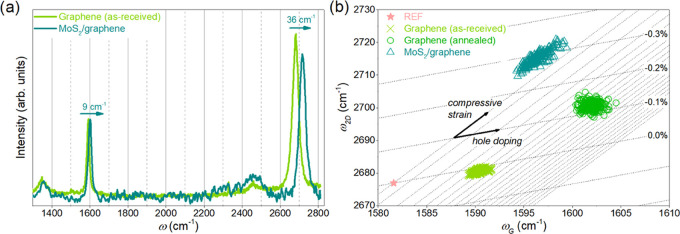
The achievement of a continuous layer enabled the statistically oriented characterization of both MoS2 and graphene. Further analyses were performed on samples with similar morphologies, as presented in Figure 6. First, we investigated changes in the structural properties of graphene induced by MoS2 growth. To confirm that graphene withstood the growth process, we have measured its Raman spectrum prior to and after the process (Figure 7a). Surprisingly, the graphene layer is virtually intact after the growth, with only changes in G and 2D peak positions, that is, approximately 9 and 36 cm–1, respectively, along with a small decrease in 2D peak amplitude. The changes in positions of graphene peaks can be used to determine strain and doping levels in graphene, according to Lee et al.51 However, at this point, it has to be noted that the absolute values of strain and doping cannot be established on a dielectric substrate, and only the relative change can be determined. It is due to dielectric screening, which reduces the electron–phonon coupling, manifested as an upshift of graphene 2D peak.52
Figure 7.
(a) Raman spectra of graphene before and after the growth on MoS2. Raman spectra are normalized to G peak, and the background has been subtracted. (b) Strain doping relation in as-received graphene, annealed graphene, and graphene with MoS2 layer grown on top of it.
The analysis of the graphene Raman peaks position is presented in Figure 7b. When MoS2 is synthesized on graphene, it can be noted that both strain and doping components are significantly changed, with higher compressive strain and lower doping. To determine the reason for these changes, we annealed the as-received graphene sample by placing the substrate in the growth chamber and applying the same growth parameters as in the standard growth run, except that we did not introduce precursors to the growth chamber.
After annealing, the graphene layer is in an intermediate strain state with slightly higher doping. One possible explanation of doping change is that during reactor heating up, moisture and other impurities desorb from graphene, which restores it to the pristine nondoped state.53 This state, however, reverts closely to the doping of the as-received graphene when exposed again to dopants from the ambient atmosphere. On the other hand, when MoS2 is grown on graphene, it acts similarly to hexagonal boron nitride (hBN)54 and encapsulates the nondoped state. As a result, graphene with MoS2 on top is low doped.
Therefore, we can conclude that the graphene layer is well preserved after the growth of the MoS2 layer. The change of the graphene doping determined via shifts of G and 2D peak positions can be explained by both thermal treatment and MoS2 encapsulation.
Raman Characterization of Continuous MoS2 on SiO2 and Graphene
Investigations of the strain level in MoS2 layers are of increasing interest as they provide insight into the tunability of the band gap of the 2D semiconductor.55 There are two main methods to characterize the strain levels in TMDCs, that is, Raman spectroscopy56 and photoluminescence.57 Several factors can impact the shift and separation of Raman peaks. Besides strain, stacking order,48 number of layers, and doping can also influence the position of the peaks. With a higher number of layers, the peak separation is increasing.6 Doping predominantly influences the A1g peak, shifting it toward higher wavenumbers with larger hole doping,58 and increase in compressive strain results mostly in the increase of E2g peak position. However, similar to graphene on a dielectric substrate, it has been shown that it is not possible to determine the absolute values of strain and doping in MoS2, and it has to be stressed that only the relative changes between two samples can be established.59
Still, the peak positions derived from Raman mapping can be used to determine the relative change in these properties. The MoS2 peak positions are presented in Figure 8. The average MoS2 peak separation on graphene is higher, reaching 22.7 cm–1, while on SiO2, this value is equal to 21.3 cm–1. As shown in Figure 6, there is a significant number of adlayers, especially in the case of the graphene sample. The spectra were collected in a statistically oriented manner with a defocused laser beam; hence, the adlayers contributed to the peak separation. Nevertheless, even if we assume a complete bilayer on graphene and a monolayer on SiO2, the contribution of adlayers does not explain the observed shift of the peaks. Therefore, also strain and doping affect the peak positions, suggesting higher tensile strain and electron doping in the SiO2 sample.
Figure 8.
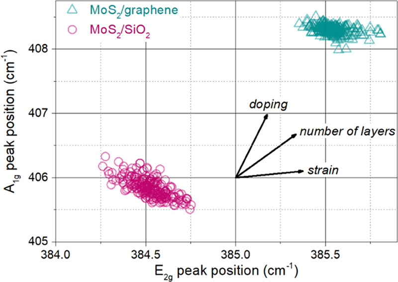
Position of MoS2 Raman peaks on graphene and SiO2.
Interestingly, the higher wavenumber of MoS2 peaks on graphene is also reported by other groups.26 Furthermore, the standard peak separation in monolayer MoS2 on SiO2 is approximately 19 cm–1,57 while the lowest reported separation for MoS2 on graphene is 20.9 cm–1,26 and other groups achieved 21.360 and 21.5 cm–1.24 It suggests that MoS2/graphene heterostructures behave differently from MoS2/SiO2, which is consistent with our hypothesis of the impact of the growth substrate.
Quantitative Determination of Strain Levels in Continuous MoS2 on SiO2 and Graphene via PL
As the Raman analysis cannot be used to arbitrarily determine the structural and electronic properties of MoS2, we measured the photoluminescence spectra of MoS2 on both samples. The PL intensity on graphene is significantly suppressed due to the photoluminescence quenching effect. It is explained by an electronic coupling between MoS2 and graphene, which results in transferring the photogenerated carriers to graphene before they recombine.17 As a result, the PL signal on graphene is much weaker, and to achieve similar intensity to the signal, we exposed the graphene sample to laser light 45 times longer than the SiO2 substrate. Any temperature-related effects have been suppressed by the defocused laser beam.
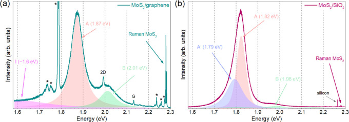
Notably, in our samples, there are multiple PL peaks, and three excitons, namely, A, B, and I, can be distinguished (Figure 9). The A and B excitons originate from the direct transitions between valence and conduction bands at the K point,7 and I is directly associated with an indirect transition from K to Γ in bilayer MoS2.57 Additionally, also a negative trion, A–,61 can be observed.
Figure 9.
Photoluminescence spectra of continuous MoS2 layer on (a) graphene and (b) SiO2. Sapphire peaks were marked with asterisks. To achieve comparable intensity, the MoS2/graphene sample was irradiated 45 times longer.
The presence of I exciton in our graphene sample is caused by a significant number of adlayers. Furthermore, the presence of A– trion in the SiO2 sample might indicate n-doping or a relatively strong MoS2–substrate interaction.18,63 As the trion is not present in the graphene sample, it indicates that the doping is at a low level caused by the lack of dopants in graphene. Simultaneously, we used n-doped SiO2, which induced electron doping of MoS2.
Finally, we observed that the position of exciton A is substantially shifted toward lower energy on SiO2. Contrary to Raman peaks, the position of the main photoluminescence peak is virtually unaffected by the number of layers,62 and the contribution of doping manifests as the presence of trions. Additionally, temperature can shift the PL peak position; however, this change is small compared to strain,64 and the majority of the research groups are measuring PL at room temperature. As a consequence, the only variable substantially influencing the exciton peak position is strain.
Numerous works are showing the impact of strain on the photoluminescence peak position.55,57,63,65,66 Interestingly, in the case of MoS2 on SiO2, the reported A exciton energy of the unstrained MoS2 is varying from 1.855 to 1.9 eV,66 and the theoretical value for the band gap in MoS2 is predicted to be 1.9 eV.62 Nevertheless, in the case of MoS2 on graphene, the reported energy of A exciton is in a much narrower range, between 1.8621 and 1.88 eV.60 Similar values of A exciton position were also measured for freestanding MoS2 monolayers, in which the influence of substrate is negligible.67
Combining all of the literature data and our observations, a clear conclusion is drawn. First of all, the van der Waals epitaxy is by definition a strain-free growth method, and the work of Liu et al.26 confirms that MoS2 grown on graphene has the same lattice constant as bulk MoS2, indicating a strain-free layer. Second, the exceptional stability of A exciton energy in MoS2/graphene systems highlights the unusual structural similarity between samples produced at different groups. Therefore, we conclude that MoS2 grown by van der Waals epitaxy on graphene is, in fact, strain-free, and the band gap energy of monolayer MoS2 is in a narrow range between 1.86 and 1.88 eV.
We also remind that the graphene layer under MoS2 is compressed, and it results directly from the epitaxial growth. Graphene on sapphire is presumably partially covalently bound to sapphire, as it is in the case of epitaxial graphene on SiC and due to similarity of the growth processes.68,69 Therefore, chemical bonds restrict the adaption of graphene to the substrate. MoS2, however, is bound only by the weak van der Waals forces, which enable better accommodation to the underlying layer. Similar observations were made by Verhagen et al.,70 who showed that the top layer of bilayer graphene is more relaxed as it can slip over the bottom graphene layer.
We also suggest that PL can be used to arbitrarily determine the strain level in MoS2. According to the work of Conley et al.,57 the value of A exciton response to strain is 45 meV/%. The thermal expansion coefficient of SiO2 is 0.5 × 10⁻⁶ K–1,71 while that of MoS2 is 17.4 × 10⁻⁶ K–1.72 In our case, the difference between growth and PL measurement temperature is 750 K; therefore, the calculated strain difference between MoS2 on graphene and SiO2 is approximately 1.27%. Simultaneously, the difference resulting from A exciton shift is 1.11%, which is in excellent agreement. The small difference between these values can be explained by the cracks of MoS2 on SiO2, partially releasing strain. It proves that the PL-based determination of strain is a viable and accessible method to establish strain levels in MoS2.
Conclusions
The direct comparison of MoS2 grown by TVD on SiO2, sapphire, and graphene showed that the growth on these substrates is governed by different surface diffusion mechanisms. On 3D substrates, it can be described as hopping between high-energy sites, while on graphene, it is characterized by the gas-molecule-collision-like mechanism. The synthesis on SiO2, as controlled by the low surface diffusion, is sensitive to even slight variations in the growth conditions. This explains the differences between results achieved by different research groups using apparently identical growth conditions. Moreover, the nature of the growth on 3D substrates can even manifest as the formation of circular domains in unfavorable thermodynamic conditions, i.e., low sulfur flux, low temperature, and low carrier gas flow.
At the same time, on graphene, the surface diffusion mechanism results in thermodynamically driven growth, leading to the formation of triangular domains only. The MoS2 growth on graphene is unusually stable and practically unaffected by the change of the growth conditions, which may be favorable for industrial-scale growth. Interestingly, graphene is virtually unchanged by the growth process, further suggesting the industrial capability of graphene as the growth platform. Also, the application of graphene as the growth substrate resulted in the realization of van der Waals epitaxy; therefore, the MoS2 layer is strain-free. The strain-free nature of MoS2 on graphene is confirmed by PL studies and supported by the literature data, and we settle the ongoing discussion of the strain levels in MoS2 on graphene. We also suggest that PL can be used to arbitrarily determine strain levels in MoS2, as we showed for MoS2 on SiO2.
Still, there is some uncertainty in several aspects of the MoS2 growth, including whether MoS2 molecules or clusters are present in the vapor phase or what is the impact of these particular species on the actual surface diffusion mechanism on a CVD graphene. To address these concerns, further theoretical research on the growth of van der Waals heterostructures is necessary.
Acknowledgments
The authors acknowledge the support of the EU Graphene Flagship funding (Grant Graphene Core3 no. 881603). This work was also partially supported by the CHARMING project (EOS 30467715), funded by Research Foundation—Flanders (G0F6218N). The research leading to these results has received funding from the PROM PW project, financed by the European Social Fund under the Operational Program Knowledge Education Development (POWR.03.03.00-00-PN13/18). The research was realized as a part of two PRELUDIUM projects (UMO-2019/33/N/ST5/01414 and UMO-2016/21/N/ST5/03332), funded by the Polish National Science Centre.
The authors declare no competing financial interest.
References
- Han S. W.; Kwon H.; Kim S. K.; Ryu S.; Yun W. S.; Kim D. H.; Hwang J. H.; Kang J. S.; Baik J.; Shin H. J.; Hong S. C. Band-Gap Transition Induced by Interlayer van der Waals Interaction in MoS2. Phys. Rev. B: Condens. Matter Mater. Phys. 2011, 84, 045409 10.1103/PhysRevB.84.045409. [DOI] [Google Scholar]
- Zhang W.; Chuu C.-P.; Huang J.-K.; Chen C.-H.; Tsai M.-L.; Chang Y.-H.; Liang C.-T.; Chen Y.-Z.; Chueh Y.-L.; He J.-H.; Chou M.-Y.; Li L.-J. Ultrahigh-Gain Photodetectors Based on Atomically Thin Graphene-MoS2 Heterostructures. Sci. Rep. 2015, 4, 3826 10.1038/srep03826. [DOI] [PMC free article] [PubMed] [Google Scholar]
- Yu W. J.; Li Z.; Zhou H.; Chen Y.; Wang Y.; Huang Y.; Duan X. Vertically Stacked Multi-Heterostructures of Layered Materials for Logic Transistors and Complementary Inverters. Nat. Mater. 2013, 12, 246–252. 10.1038/nmat3518. [DOI] [PMC free article] [PubMed] [Google Scholar]
- Roy K.; Padmanabhan M.; Goswami S.; Sai T. P.; Ramalingam G.; Raghavan S.; Ghosh A. Graphene-MoS2 Hybrid Structures for Multifunctional Photoresponsive Memory Devices. Nat. Nanotechnol. 2013, 8, 826–830. 10.1038/nnano.2013.206. [DOI] [PubMed] [Google Scholar]
- Withers F.; Del Pozo-Zamudio O.; Mishchenko A.; Rooney A. P.; Gholinia A.; Watanabe K.; Taniguchi T.; Haigh S. J.; Geim A. K.; Tartakovskii A. I.; Novoselov K. S. Light-Emitting Diodes by Band-Structure Engineering in van der Waals Heterostructures. Nat. Mater. 2015, 14, 301–306. 10.1038/nmat4205. [DOI] [PubMed] [Google Scholar]
- Lee C.; Yan H.; Brus L. E.; Heinz T. F.; Hone J.; Ryu S. Anomalous Lattice Vibrations of Single- and Few-Layer MoS2. ACS Nano 2010, 4, 2695–2700. 10.1021/nn1003937. [DOI] [PubMed] [Google Scholar]
- Van Der Zande A. M.; Huang P. Y.; Chenet D. A.; Berkelbach T. C.; You Y.; Lee G. H.; Heinz T. F.; Reichman D. R.; Muller D. A.; Hone J. C. Grains and Grain Boundaries in Highly Crystalline Monolayer Molybdenum Disulphide. Nat. Mater. 2013, 12, 554–561. 10.1038/nmat3633. [DOI] [PubMed] [Google Scholar]
- Kim H.; Ovchinnikov D.; Deiana D.; Unuchek D.; Kis A. Suppressing Nucleation in Metal-Organic Chemical Vapor Deposition of MoS2 Monolayers by Alkali Metal Halides. Nano Lett. 2017, 17, 5056–5063. 10.1021/acs.nanolett.7b02311. [DOI] [PubMed] [Google Scholar]
- Dumcenco D.; Ovchinnikov D.; Marinov K.; Lazić P.; Gibertini M.; Marzari N.; Sanchez O. L.; Kung Y. C.; Krasnozhon D.; Chen M. W.; Bertolazzi S.; Gillet P.; Funtcuberta i Morral A.; Radenovic A.; Kis A. Large-Area Epitaxial Monolayer MoS2. ACS Nano 2015, 9, 4611–4620. 10.1021/acsnano.5b01281. [DOI] [PMC free article] [PubMed] [Google Scholar]
- Nakamura S.; Harada Y.; Seno M. Novel Metalorganic Chemical Vapor Deposition System for GaN Growth. Appl. Phys. Lett. 1991, 58, 2021–2023. 10.1063/1.105239. [DOI] [Google Scholar]
- Mishra N.; Forti S.; Fabbri F.; Martini L.; McAleese C.; Conran B. R.; Whelan P. R.; Shivayogimath A.; Jessen B. S.; Buß L.; Falta J.; Aliaj I.; Roddaro S.; Flege J. I.; Bøggild P.; Teo K. B. K.; Coletti C. Wafer-Scale Synthesis of Graphene on Sapphire: Toward Fab-Compatible Graphene. Small 2019, 1904906 10.1002/smll.201904906. [DOI] [PubMed] [Google Scholar]
- Cun H.; Macha M.; Kim H. K.; Liu K.; Zhao Y.; LaGrange T.; Kis A.; Radenovic A. Wafer-Scale MOCVD Growth of Monolayer MoS2 on Sapphire and SiO2. Nano Res. 2019, 12, 2646–2652. 10.1007/s12274-019-2502-9. [DOI] [Google Scholar]
- Geim A. K.; Grigorieva I. V. Van der Waals Heterostructures. Nature 2013, 499, 419–425. 10.1038/nature12385. [DOI] [PubMed] [Google Scholar]
- Wan W.; Li X.; Li X.; Xu B.; Zhan L.; Zhao Z.; Zhang P.; Wu S. Q.; Zhu Z. Z.; Huang H.; Zhou Y.; Cai W. Interlayer Coupling of a Direct van der Waals Epitaxial MoS2/Graphene Heterostructure. RSC Adv. 2016, 6, 323–330. 10.1039/C5RA22768B. [DOI] [Google Scholar]
- Yue R.; Nie Y.; Walsh L. A.; Addou R.; Liang C.; Lu N.; Barton A. T.; Zhu H.; Che Z.; Barrera D.; Cheng L.; Cha P.-R.; Chabal Y. J.; Hsu J. W. P.; Kim J.; Kim M. J.; Colombo L.; Wallace R. M.; Cho K.; Hinkle C. L. Nucleation and Growth of WSe2: Enabling Large Grain Transition Metal Dichalcogenides. 2D Mater. 2017, 4, 045019 10.1088/2053-1583/aa8ab5. [DOI] [Google Scholar]
- Ago H.; Endo H.; Solís-Fernández P.; Takizawa R.; Ohta Y.; Fujita Y.; Yamamoto K.; Tsuji M. Controlled van der Waals Epitaxy of Monolayer MoS2 Triangular Domains on Graphene. ACS Appl. Mater. Interfaces 2015, 7, 5265–5273. 10.1021/am508569m. [DOI] [PubMed] [Google Scholar]
- Azizi A.; Eichfeld S.; Geschwind G.; Zhang K.; Jiang B.; Mukherjee D.; Hossain L.; Piasecki A. F.; Kabius B.; Robinson J. A.; Alem N. Freestanding van der Waals Heterostructures of Graphene and Transition Metal Dichalcogenides. ACS Nano 2015, 9, 4882–4890. 10.1021/acsnano.5b01677. [DOI] [PubMed] [Google Scholar]
- Chen T.; Zhou Y.; Sheng Y.; Wang X.; Zhou S.; Warner J. H. Hydrogen-Assisted Growth of Large-Area Continuous Films of MoS2 on Monolayer Graphene. ACS Appl. Mater. Interfaces 2018, 10, 7304–7314. 10.1021/acsami.7b14860. [DOI] [PubMed] [Google Scholar]
- Pierucci D.; Henck H.; Naylor C. H.; Sediri H.; Lhuillier E.; Balan A.; Rault J. E.; Dappe Y. J.; Bertran F.; Fèvre P. L.; Johnson A. T. C.; Ouerghi A. Large Area Molybdenum Disulphide-Epitaxial Graphene Vertical van der Waals Heterostructures. Sci. Rep. 2016, 6, 26656 10.1038/srep26656. [DOI] [PMC free article] [PubMed] [Google Scholar]
- Shi Y.; Zhou W.; Lu A.-Y.; Fang W.; Lee Y.-H.; Hsu A. L.; Kim S. M.; Kim K. K.; Yang H. Y.; Li L.-J.; Idrobo J.-C.; Kong J. Van der Waals Epitaxy of MoS2 Layers Using Graphene As Growth Templates. Nano Lett. 2012, 12, 2784–2791. 10.1021/nl204562j. [DOI] [PubMed] [Google Scholar]
- Shi J.; Liu M.; Wen J.; Ren X.; Zhou X.; Ji Q.; Ma D.; Zhang Y.; Jin C.; Chen H.; Deng S.; Xu N.; Liu Z.; Zhang Y. All Chemical Vapor Deposition Synthesis and Intrinsic Bandgap Observation of MoS2/Graphene Heterostructures. Adv. Mater. 2015, 27, 7086–7092. 10.1002/adma.201503342. [DOI] [PubMed] [Google Scholar]
- Wan W.; Chen L.; Zhan L.; Zhu Z.; Zhou Y.; Shih T.; Guo S.; Kang J.; Huang H.; Cai W. Syntheses and Bandgap Alterations of MoS2 Induced by Stresses in Graphene-Platinum Substrates. Carbon 2018, 131, 26–30. 10.1016/j.carbon.2018.01.085. [DOI] [Google Scholar]
- Lin M.-Y.; Chang C.-E.; Wang C.-H.; Su C.-F.; Chen C.; Lee S.-C.; Lin S.-Y. Toward Epitaxially Grown Two-Dimensional Crystal Hetero-Structures: Single and Double MoS2/Graphene Hetero-Structures by Chemical Vapor Depositions. Appl. Phys. Lett. 2014, 105, 073501 10.1063/1.4893448. [DOI] [Google Scholar]
- Chen H. A.; Chen W. C.; Sun H.; Lin C. C.; Lin S. Y. Scalable MoS2/Graphene Hetero-Structures Grown Epitaxially on Sapphire Substrates for Phototransistor Applications. Semicond. Sci. Technol. 2018, 33, 025007 10.1088/1361-6641/aaa3b7. [DOI] [Google Scholar]
- Miwa J. A.; Dendzik M.; Grønborg S. S.; Bianchi M.; Lauritsen J. V.; Hofmann P.; Ulstrup S. Van der Waals Epitaxy of Two-Dimensional MoS2-Graphene Heterostructures in Ultrahigh Vacuum. ACS Nano 2015, 9, 6502–6510. 10.1021/acsnano.5b02345. [DOI] [PubMed] [Google Scholar]
- Liu X.; Balla I.; Bergeron H.; Campbell G. P.; Bedzyk M. J.; Hersam M. C. Rotationally Commensurate Growth of MoS2 on Epitaxial Graphene. ACS Nano 2016, 10, 1067–1075. 10.1021/acsnano.5b06398. [DOI] [PubMed] [Google Scholar]
- Liu X.; Balla I.; Bergeron H.; Hersam M. C. Point Defects and Grain Boundaries in Rotationally Commensurate MoS2 on Epitaxial Graphene. J. Phys. Chem. C 2016, 120, 20798–20805. 10.1021/acs.jpcc.6b02073. [DOI] [Google Scholar]
- Judek J.; Gertych A. P.; Czerniak K.; Zdrojek M. Temperature Dependence of Phonon Properties in CVD MoS2 Nanostructures – a Statistical Approach. Phys. Chem. Chem. Phys. 2018, 20, 15486–15495. 10.1039/C8CP01232F. [DOI] [PubMed] [Google Scholar]
- Ji Q.; Zhang Y.; Gao T.; Zhang Y.; Ma D.; Liu M.; Chen Y.; Qiao X.; Tan P. H.; Kan M.; Feng J.; Sun Q.; Liu Z. Epitaxial Monolayer MoS2 on Mica with Novel Photoluminescence. Nano Lett. 2013, 13, 3870–3877. 10.1021/nl401938t. [DOI] [PubMed] [Google Scholar]
- Steudel R.; Steudel Y.; Wong M. W.. Speciation and Thermodynamics of Sulfur Vapor. Elemental Sulfur and Sulfur-Rich Compounds I; Steudel R., Ed.; Springer: Berlin, Heidelberg, 2003; pp 117–134. [Google Scholar]
- Berkowitz J.; Inghram M. G.; Chupka W. A. Polymeric Gaseous Species in the Sublimation of Molybdenum Trioxide. J. Chem. Phys. 1957, 26, 842–846. 10.1063/1.1743417. [DOI] [Google Scholar]
- Fialko E. F.; Kikhtenko A. V.; Goncharov V. B.; Zamaraev K. I. Molybdenum Oxide Cluster Ions in the Gas Phase: Structure and Reactivity with Small Molecules. J. Phys. Chem. A 1997, 101, 8607–8613. 10.1021/jp971585v. [DOI] [Google Scholar]
- Yu Y.; Li C.; Liu Y.; Su L.; Zhang Y.; Cao L. Controlled Scalable Synthesis of Uniform, High-Quality Monolayer and Few-Layer MoS2 Films. Sci. Rep. 2013, 3, 1866 10.1038/srep01866. [DOI] [PMC free article] [PubMed] [Google Scholar]
- Stull D. R. Inorganic Compounds. Ind. Eng. Chem. 1947, 39, 540–550. 10.1021/ie50448a023. [DOI] [Google Scholar]
- Rau H.; Kutty T. R. N.; Guedes de Carvalho J. R. F. High Temperature Saturated Vapour Pressure of Sulphur and the Estimation of Its Critical Quantities. J. Chem. Thermodyn. 1973, 5, 291–302. 10.1016/S0021-9614(73)80089-8. [DOI] [Google Scholar]
- Bisson E. E.Lubrication and Bearing Problems in the Vacuum of Space; NASA Lewis Research Center Cleveland, 1966. [Google Scholar]
- Walsh L. A.; Hinkle C. L. Van der Waals Epitaxy: 2D Materials and Topological Insulators. Appl. Mater. Today 2017, 9, 504–515. 10.1016/j.apmt.2017.09.010. [DOI] [Google Scholar]
- Koma A. Van der Waals Epitaxy – a New Epitaxial Growth Method for a Highly Lattice-Mismatched System. Thin Solid Films 1992, 216, 72–76. 10.1016/0040-6090(92)90872-9. [DOI] [Google Scholar]
- Ehrlich G.; Stolt K. Surface Diffusion. Annu. Rev. Phys. Chem. 1980, 31, 603–637. 10.1146/annurev.pc.31.100180.003131. [DOI] [Google Scholar]
- Kataria S.; Wagner S.; Cusati T.; Fortunelli A.; Iannaccone G.; Pandey H.; Fiori G.; Lemme M. C. Growth-Induced Strain in Chemical Vapor Deposited Monolayer MoS2: Experimental and Theoretical Investigation. Adv. Mater. Interfaces 2017, 4, 1700031 10.1002/admi.201700031. [DOI] [Google Scholar]
- Dash J. G.; Ruvalds J.. Phase Transitions in Surface Films; Dash J. G., Ruvalds J., Eds.; Springer US: Boston, MA, 1980. [Google Scholar]
- Oura K.; Katayama M.; Zotov A. V.; Lifshits V. G.; Saranin A. A.. Surface Science: An Introduction; Advanced Texts in Physics; Springer: Berlin, Heidelberg, 2003. [Google Scholar]
- Sun C.; Bai B. Gas Diffusion on Graphene Surfaces. Phys. Chem. Chem. Phys. 2017, 19, 3894–3902. 10.1039/C6CP06267A. [DOI] [PubMed] [Google Scholar]
- Persson M.; Andersson S.. Physisorption Dynamics at Metal Surfaces. Handbook of Surface Science; Elsevier, 2008; Vol. 3, pp 95–139. [Google Scholar]
- Suzanne J.; Gay J. M.. The Structure of Physically Adsorbed Phases. Handbook of Surface Science; Elsevier, 1996; Vol. 1, pp 503–575. [Google Scholar]
- Cao D.; Shen T.; Liang P.; Chen X.; Shu H. Role of Chemical Potential in Flake Shape and Edge Properties of Monolayer MoS2. J. Phys. Chem. C 2015, 119, 4294–4301. 10.1021/jp5097713. [DOI] [Google Scholar]
- Wang S.; Rong Y.; Fan Y.; Pacios M.; Bhaskaran H.; He K.; Warner J. H. Shape Evolution of Monolayer MoS2 Crystals Grown by Chemical Vapor Deposition. Chem. Mater. 2014, 26, 6371–6379. 10.1021/cm5025662. [DOI] [Google Scholar]
- Shinde S. M.; Dhakal K. P.; Chen X.; Yun W. S.; Lee J.; Kim H.; Ahn J.-H. Stacking-Controllable Interlayer Coupling and Symmetric Configuration of Multilayered MoS2. NPG Asia Mater. 2018, 10, e468–e468. 10.1038/am.2017.226. [DOI] [Google Scholar]
- Zhang J.; Yu H.; Chen W.; Tian X.; Liu D.; Cheng M.; Xie G.; Yang W.; Yang R.; Bai X.; Shi D.; Zhang G. Scalable Growth of High-Quality Polycrystalline MoS2 Monolayers on SiO2 with Tunable Grain Sizes. ACS Nano 2014, 8, 6024–6030. 10.1021/nn5020819. [DOI] [PubMed] [Google Scholar]
- Wan W.; Zhan L.; Xu B.; Zhao F.; Zhu Z.; Zhou Y.; Yang Z.; Shih T.; Cai W. Temperature-Related Morphological Evolution of MoS2 Domains on Graphene and Electron Transfer within Heterostructures. Small 2017, 13, 1603549 10.1002/smll.201603549. [DOI] [PubMed] [Google Scholar]
- Lee J. E.; Ahn G.; Shim J.; Lee Y. S.; Ryu S. Optical Separation of Mechanical Strain from Charge Doping in Graphene. Nat. Commun. 2012, 3, 1024 10.1038/ncomms2022. [DOI] [PubMed] [Google Scholar]
- Forster F.; Molina-Sanchez A.; Engels S.; Epping A.; Watanabe K.; Taniguchi T.; Wirtz L.; Stampfer C. Dielectric Screening of the Kohn Anomaly of Graphene on Hexagonal Boron Nitride. Phys. Rev. B: Condens. Matter Mater. Phys. 2013, 88, 085419 10.1103/PhysRevB.88.085419. [DOI] [Google Scholar]
- Tsukamoto T.; Yamazaki K.; Komurasaki H.; Ogino T. Effects of Surface Chemistry of Substrates on Raman Spectra in Graphene. J. Phys. Chem. C 2012, 116, 4732–4737. 10.1021/jp2113158. [DOI] [Google Scholar]
- Banszerus L.; Schmitz M.; Engels S.; Dauber J.; Oellers M.; Haupt F.; Watanabe K.; Taniguchi T.; Beschoten B.; Stampfer C. Ultrahigh-Mobility Graphene Devices from Chemical Vapor Deposition on Reusable Copper. Sci. Adv. 2015, 1, e1500222 10.1126/sciadv.1500222. [DOI] [PMC free article] [PubMed] [Google Scholar]
- Hui Y. Y.; Liu X.; Jie W.; Chan N. Y.; Hao J.; Hsu Y.-T.; Li L.-J. J.; Guo W.; Lau S. P. Exceptional Tunability of Band Energy in a Compressively Strained Trilayer MoS2 Sheet. ACS Nano 2013, 7, 7126–7131. 10.1021/nn4024834. [DOI] [PubMed] [Google Scholar]
- Rice C.; Young R. J.; Zan R.; Bangert U.; Wolverson D.; Georgiou T.; Jalil R.; Novoselov K. S. Raman-Scattering Measurements and First-Principles Calculations of Strain-Induced Phonon Shifts in Monolayer MoS2. Phys. Rev. B: Condens. Matter Mater. Phys. 2013, 87, 081307 10.1103/PhysRevB.87.081307. [DOI] [Google Scholar]
- Conley H. J.; Wang B.; Ziegler J. I.; Haglund R. F.; Pantelides S. T.; Bolotin K. I. Bandgap Engineering of Strained Monolayer and Bilayer MoS2. Nano Lett. 2013, 13, 3626–3630. 10.1021/nl4014748. [DOI] [PubMed] [Google Scholar]
- Chakraborty B.; Bera A.; Muthu D. V. S.; Bhowmick S.; Waghmare U. V.; Sood A. K. Symmetry-Dependent Phonon Renormalization in Monolayer MoS2 Transistor. Phys. Rev. B: Condens. Matter Mater. Phys. 2012, 85, 161403 10.1103/PhysRevB.85.161403. [DOI] [Google Scholar]
- Michail A.; Delikoukos N.; Parthenios J.; Galiotis C.; Papagelis K. Optical Detection of Strain and Doping Inhomogeneities in Single Layer MoS2. Appl. Phys. Lett. 2016, 108, 173102 10.1063/1.4948357. [DOI] [Google Scholar]
- McCreary K. M.; Hanbicki A. T.; Robinson J. T.; Cobas E.; Culbertson J. C.; Friedman A. L.; Jernigan G. G.; Jonker B. T. Large-Area Synthesis of Continuous and Uniform MoS2 Monolayer Films on Graphene. Adv. Funct. Mater. 2014, 24, 6449–6454. 10.1002/adfm.201401511. [DOI] [Google Scholar]
- Mak K. F.; He K.; Lee C.; Lee G. H.; Hone J.; Heinz T. F.; Shan J. Tightly Bound Trions in Monolayer MoS2. Nat. Mater. 2013, 12, 207–211. 10.1038/nmat3505. [DOI] [PubMed] [Google Scholar]
- Mak K. F.; Lee C.; Hone J.; Shan J.; Heinz T. F. Atomically Thin MoS2: A New Direct-Gap Semiconductor. Phys. Rev. Lett. 2010, 105, 2–5. 10.1103/PhysRevLett.105.136805. [DOI] [PubMed] [Google Scholar]
- Dubey S.; Lisi S.; Nayak G.; Herziger F.; Nguyen V.; Le Quang T.; Cherkez V.; González C.; Dappe Y. J.; Watanabe K.; Taniguchi T.; Magaud L.; Mallet P.; Veuillen J.-Y.; Arenal R.; Marty L.; Renard J.; Bendiab N.; Coraux J.; Bouchiat V. Weakly Trapped, Charged, and Free Excitons in Single-Layer MoS2 in the Presence of Defects, Strain, and Charged Impurities. ACS Nano 2017, 11, 11206–11216. 10.1021/acsnano.7b05520. [DOI] [PubMed] [Google Scholar]
- Tongay S.; Zhou J.; Ataca C.; Lo K.; Matthews T. S.; Li J.; Grossman J. C.; Wu J. Thermally Driven Crossover from Indirect toward Direct Bandgap in 2D Semiconductors: MoSe2 versus MoS2. Nano Lett. 2012, 12, 5576–5580. 10.1021/nl302584w. [DOI] [PubMed] [Google Scholar]
- Castellanos-Gomez A.; Roldán R.; Cappelluti E.; Buscema M.; Guinea F.; Van Der Zant H. S. J.; Steele G. A. Local Strain Engineering in Atomically Thin MoS2. Nano Lett. 2013, 13, 5361–5366. 10.1021/nl402875m. [DOI] [PubMed] [Google Scholar]
- Niehues I.; Blob A.; Stiehm T.; Schmidt R.; Jadriško V.; Radatović B.; Čapeta D.; Kralj M.; de Vasconcellos S. M.; Bratschitsch R. Strain Transfer across Grain Boundaries in MoS2 Monolayers Grown by Chemical Vapor Deposition. 2D Mater. 2018, 5, 031003 10.1088/2053-1583/aaba9a. [DOI] [Google Scholar]
- Scheuschner N.; Ochedowski O.; Kaulitz A. M.; Gillen R.; Schleberger M.; Maultzsch J. Photoluminescence of Freestanding Single- and Few-Layer MoS2. Phys. Rev. B: Condens. Matter Mater. Phys. 2014, 89, 125406 10.1103/PhysRevB.89.125406. [DOI] [Google Scholar]
- Emtsev K. V.; Speck F.; Seyller T.; Ley L.; Riley J. D. Interaction, Growth, and Ordering of Epitaxial Graphene on SiC{0001} Surfaces: A Comparative Photoelectron Spectroscopy Study. Phys. Rev. B: Condens. Matter Mater. Phys. 2008, 77, 155303 10.1103/PhysRevB.77.155303. [DOI] [Google Scholar]
- Strupinski W.; Grodecki K.; Wysmolek A.; Stepniewski R.; Szkopek T.; Gaskell P. E.; Grüneis A.; Haberer D.; Bozek R.; Krupka J.; Baranowski J. M. Graphene Epitaxy by Chemical Vapor Deposition on SiC. Nano Lett. 2011, 11, 1786–1791. 10.1021/nl200390e. [DOI] [PubMed] [Google Scholar]
- Verhagen T. G. A.; Drogowska K.; Kalbac M.; Vejpravova J. Temperature-Induced Strain and Doping in Monolayer and Bilayer Isotopically Labeled Graphene. Phys. Rev. B: Condens. Matter Mater. Phys. 2015, 92, 1–9. 10.1103/PhysRevB.92.125437. [DOI] [Google Scholar]
- Tada H.; Kumpel A. E.; Lathrop R. E.; Slanina J. B.; Nieva P.; Zavracky P.; Miaoulis I. N.; Wong P. Y. Thermal Expansion Coefficient of Polycrystalline Silicon and Silicon Dioxide Thin Films at High Temperatures. J. Appl. Phys. 2000, 87, 4189–4193. 10.1063/1.373050. [DOI] [Google Scholar]
- Peng B.; Zhang H.; Shao H.; Xu Y.; Zhang X.; Zhu H. Thermal Conductivity of Monolayer MoS2, MoSe2, and WS2: Interplay of Mass Effect, Interatomic Bonding and Anharmonicity. RSC Adv. 2016, 6, 5767–5773. 10.1039/C5RA19747C. [DOI] [Google Scholar]


