

Graphical abstract

Keywords: 3D-printing, Microdroplet cell, Simultaneous anodizing, Porous alumina lines, Layered structure
Abstract
Introduction
Recent advancements in 3D printing technology allow us to design and fabricate customized droplets cells for localized electrochemical patterning.
Objectives
In this study, 3D printed solution-flow type microdroplet cell (Sf-MDC) is proposed for localized anodizing of two different regions on Al surface. The effect of printing orientation on 3D printing parameters is elucidated to minimize the resin consumption, printing time and material wastage. The capability of Sf-MDC to fabricate porous alumina patterns with adjustable pore size and thickness is explored by varying the length of Pt wire inside each capillary.
Methods
The Sf-MDC was optimally fabricated using 3D printer at the highest possible resolution. The Al specimens were electropolished in 13.6 kmolm−3 CH3COOH/2.56 kmolm−3 HClO4 at 278 K and 28 V for 145 s. 0.22 kmolm−3 oxalic acid (COOH)2 solution was prepared for anodizing. The specimen was set on pulse-XYZ stage controller and anodized (at 50 V and 323 K) using the Sf-MDC.
Results
Anodizing with Sf-MDC resulted in the formation of two uniformly sized porous alumina lines on the specimen. Porous alumina lines exhibited similar pore geometry, interpore distance and pores arrangement, suggesting uniform supply of current to both the droplets. Layered-type cross-sectional structure with each layer having a thickness of 2.7 mm was formed for both the porous alumina lines. By varying the length of Pt wire inside each capillary, porous alumina lines with different porous structure and oxide thickness were simultaneously fabricated.
Conclusions
Simultaneous anodizing with Sf-MDC can be applied for fast fabrication of porous alumina filters with different porous structure and for various patterning applications.
Introduction
Development of cost-effective technologies for fast fabrication of micro-sized structures on various substrates is of paramount importance for the production of integrated circuits, microelectromechanical systems (MEMS) and biomedical devices [1], [2], [3], [4], [5], [6]. Traditional lithographic, masking and subtractive manufacturing techniques are well-established for the fabrication of micro-sized structures on desired substrates but involve multiple steps and result in significant material wastage [7], [8], [9]. Recently, localized electrochemical fabrication techniques such as scanning electrochemical microscopy (SECM), atomic force microscope (AFM) and scanning tunneling microscopy (STM) have been applied to selectively characterize and fabricate minute structures on specimen surfaces at desired areas [10], [11], [12], [13]. These techniques are preferable over conventional lithographic and masking methods since the specimen needs no initial preparation, small quantity of electrolyte is required, and precisely defined area is wetted.
Localized anodizing of metal surfaces using electrochemical droplet cell techniques is of prime importance for the fabrication of thin film capacitors, resistors, electronic circuits, interconnects and porous alumina filters [14], [15], [16], [17]. Two types of electrochemical droplet cells, i.e. scanning droplet cells [18], [19], [20] and solution flow type microdroplet cells [21], [22], [23] are commonly used for area-selective anodizing. Recently, Hassel and co-workers have used scanning droplet cell to form anodic oxide lines on Al and Ti specimen for the fabrication of resistors, capacitors, transistors, diodes, rectifiers and memristors [24]. Fabrication of anodic oxide lines with scanning droplet cells having no solution outlet is challenging in terms of synchronizing the rate of electrolyte consumption with droplet movement for each anodizing voltage. To avoid this difficulty, Sakairi et al. developed a dual capillary solution flow type microdroplet cell for the fabrication of localized porous alumina lines and through-hole porous alumina membranes [25]. This type of dual capillary design allowed continuous supply and removal of the solution during anodizing. Nevertheless, multiple steps involved during the cell fabrication, along with slow oxide fabrication speed, limit the use of this technique for practical applications. A high-throughput technique for fast fabrication of anodic oxide lines on metal substrates using electrochemical droplet cells would be needed for their future applications [26], [27], [28].
With significant advancements in 3D printing technology, it is possible to design and fabricate customized electrochemical droplets cells. Polymeric materials having good mechanical and chemical stability, e.g. polycarbonate (PC), polyamides (PA) and acrylonitrile butadiene styrene (ABS) are available for 3D printing [29], [30]. Various computer aided design (CAD) softwares can be used to design complex electrochemical flow cells with precise dimensions. CAD drawing is then converted to stereolithography (.STL) file format for 3D printing [31]. Fabrication of droplet cells using 3D printing is time saving and cost-effective because multiple cells can be printed at once with minimum usage of polymer resin. A few studies are available on the fabrication of 3D printed scanning droplet cells [20], [32], [33] and solution flow type microdroplet cell [34] for area selective anodizing. However, 3D printed scanning droplet cells used gaskets which restricted the movement of droplet during anodizing. The minimum anodizing width of about 1 mm is achieved using solution flow type microdroplet cell. Further reduction in the width of anodized lines by controlling the droplet size would be desirable for a broad range of pattering applications.
In this study, a 3D printed solution-flow type microdroplet cell (Sf-MDC) is proposed for simultaneous anodizing of two different regions on Al surface. The effect of orientation on 3D printing parameters has also been elucidated to minimize the printing time and material wastage. The fabricated Sf-MDC is applied to form two porous alumina lines simultaneously on the specimen. The influence of moving speed on the width of anodized lines is studied in relation with distance between the capillary tip and the specimen. An attempt is made to fabricate porous alumina lines with different porous structure by varying the length of Pt wire inside each capillary.
Experimental
Specimen and solution
Aluminium sheets (99.99 mass% and 110 µm thickness) were used as specimen. The sheets were cut to dimensions of 20 × 30 mm and were ultrasonically cleaned in ethanol and in highly purified water, each for 300 s. The specimens were then electropolished in 13.6 kmol m−3 acetic acid (CH3COOH)/2.56 kmol m−3 perchloric acid (HClO4) at 278 K and 28 V for 145 s. After electropolishing, the specimens were cleaned with highly purified water and acetone. As anodizing electrolyte, 0.22 kmol m−3 oxalic acid (COOH)2 solution was prepared. All chemicals were purchased from Kanto Chemical Co. Ltd, Tokyo, Japan.
Description of Sf-MDC
Double capillary Sf-MDC was designed on Solidworks CAD software and fabricated using a stereolithography type 3D-printer (Formlabs form 2, USA) at the highest possible resolution of 0.1 mm. Fig. 1 shows the scheme for the fabrication of Sf-MDC, cell dimensions and schematic representation of solution flow inside Sf-MDC. 3D-printed parts having two outer capillaries, single solution inlet and a joint counter electrode connector are shown in Fig. 1(a). After trimming the support structure, inner capillaries with Pt wires were inserted inside the outer capillaries and connected with a common counter electrode (Pt wire) to make Sf-MDC. Fig. 1(b) shows the inside view and dimensions of Sf-MDC used in this study. Schematic representation of solution flow inside Sf-MDC is shown in Fig. 1(c). Fresh solution is continuously supplied by a peristaltic pump. The solution flows inside the cell and forms droplets at both the inner capillary tips. The outer capillaries remove the used solution through 1 mm holes at their center with a vacuum pump. Inner and outer capillaries have an inside diameter of 100 µm and 500 µm, respectively.
Fig. 1.

Scheme for the fabrication of Sf-MDC, (a), inside view and dimensions of Sf-MDC, (b), schematic representation of solution flow using Sf-MDC, (c).
This type of cell design allows free movement of droplets throughout the anodizing process and thereby, desired anodic oxide patterns can be fabricated. The dual electrolyte flow channels increase the rate of oxide formation which reduces the time needed for anodizing multiple areas. A common counter electrode, single inlet and outlet supplies for both the capillaries eliminates the need of additional power supplies and pumps and save cost unlike previous designs [32], [34].
Anodizing with Sf-MDC
The schematic of anodizing setup is shown in Fig. 2. An electropolished Al specimen was set on pulse-XYZ stage controlled with computer. The specimen temperature was controlled at 323 K by a Peltier device. The Sf-MDC was filled with 0.22 kmol m−3 (COOH)2 electrolyte at a flow rate of 1.59 × 10⁻⁹ m3 s−1 by a peristaltic pump. Electrolyte droplets were allowed to form at the tip of both inner capillaries and a vacuum pressure of 85 kPa was set for the removal of depleted solution through the outer capillaries. For the operation of cell in free-mode, distance between the inner capillary tips and the specimen surface was adjusted to 30 µm. The specimen was anodized at 50 V at stage moving speed of 2 µm s−1 for the simultaneous formation of oxide lines on the specimen.
Fig. 2.

Schematic drawing of anodizing setup.
Observations
The surfaces of anodized specimens were investigated with an optical microscope (Waymaer Inc., BM-3400T) and a scanning electron microscope (SEM, JOEL Ltd., Tokyo, Japan, JSM-6510LA). Cross-sections of the anodized lines were observed by SEM after carefully curving and breaking the Al specimen. Thin Au layer was sputtered on the specimens prior to SEM observations (Fin coater, JOEL Ltd., Tokyo, Japan).
Results and discussion
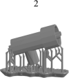
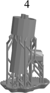
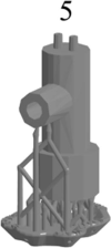
Using the dual capillary head Sf-MDC, fabrication of thin walls with circular holes within the 3D structure is challenging and is related with printing orientation. The orientation is also directly related with printing quality, printing time, printing volume and number of layers required during printing [35]. Here, an orientation study was carried out to improve the printing parameters and to obtain the good quality Sf-MDC, capable of forming porous alumina lines simultaneously. Table 1 shows the printing parameters at different orientations. The marked areas in orientation 1 indicate that part needs more supports at that area and is unable to print. Orientation 2 and orientation 3 also have missing supports at desired areas and are unprintable. More number of supports enhance the possibility of successful printing. Location and number of supports are determined by the printing software and is linked with size, weight and orientation of the part to be printed. Orientation 4 and orientation 5 are both vertically aligned, have uniform distribution of support structure and show good printability. The only difference is the volume of resin required for printing. Fig. 3(a) shows the image of vertically oriented 3D printed parts. The magnified view of capillaries after trimming the support structure is shown in Fig. 3(b). It can be seen that both capillaries in orientation 4 show blockage and cannot be used for simultaneous area selective anodizing. The capillaries in orientation 5 show through-holes, good printability and minimum resin consumption. Therefore, orientation 5 is selected as the most suitable orientation to fabricate the Sf-MDC. It is worth mentioning that the problems faced with failure of the fabrication and functioning of such droplet cells for high-throughput capabilities need extensive experimentation along with CFD simulations. A separate study will be carried out in future to address these problems.
Table 1.
Printing parameters at different orientations for optimizing the print quality.
| Orientation |  |
 |
 |
 |
 |
|---|---|---|---|---|---|
| Printing time | 60 min | 90 min | 90 min | 105 min | 105 min |
| Resin Volume | 3.42 mL | 3.39 mL | 3.67 mL | 3.79 mL | 3.19 mL |
| Number of layers | 220 | 348 | 409 | 441 | 441 |
| Printability | None | None | None | Good | Good |
Fig. 3.

Images of 3D-printed parts with vertical orientation, (a), and magnified view of capillaries after trimming the support structure, (b).
Fig. 4(a) and (b) shows optical microscope images of the simultaneously anodized lines formed with Sf-MDC. The anodized areas are clearly distinguishable from Al specimen due to a difference in refractive index of Al2O3 and Al. The length and width of the anodized lines is about 2085 µm and 470 µm, respectively. The slight increase in anodizing length as compared to scanning distance (2000 µm) is due to spherical shape of the droplets which are being dragged during the anodizing process at scanning speed of 2 µm s−1 (Fig. 4(c)). If the scanning distance of 2000 µm is assumed from the center of initial position of the droplets to their final position and considering the diameter of droplets to be around 470 µm, a total anodized length should be around 2470 µm. However, the direction of the droplets movement during anodizing and solution removal from the outer capillary by the vacuum pump shifts the position of the droplets from the center as shown in Fig. 4(c). This results in anodized lines of length 2085 µm. Because of capillary forces present between the Al surface and tips of inner capillaries, electrolyte droplets and the capillary tips move together during scanning. The width of anodized lines (470 µm) was greater than the diameter of inner capillaries (100 µm), however, smaller than the diameter of outer capillaries (500 µm). Some fuzzy marks are observable outside the anodizing area. This may be caused by droplets movement in a discrete manner instead of continuous wetting mechanism. The capillary and surface tension forces are trying to counterbalance each other during scanning while vacuum pressure is forcing the used solution to flow back from outer capillaries. As a result, some fluid spreads outside the concentrated region. The length of anodized lines can be increased or decreased by changing the scanning distance using XYZ stage controller. The width of anodized lines can be controlled by increasing the scanning speed. Fig. 5 shows the influence of moving speed on the width of anodized line in relation with distance between the capillary tip and the specimen (Ht). For simplicity, only a single porous alumina line was formed on the specimen. It can be seen that width of anodized line decreases by increasing the scanning speed. The average width of anodized line is 810 µm at scanning speed of 1 µm s−1 and Ht = 30 µm. A sudden decrease in the width of anodized line is observed as the scanning speed is increased to 2 µm s−1. This is due to a decrease in the scanning time which allows the droplet to move faster during anodizing. Considering the fact that electrocapillarity plays a key role to reach the surface tension equilibrium [19], a faster movement of Sf-MDC will result in continuous motion of droplet and maintains the surface tension of the electrolyte without allowing the droplet to expand in the lateral direction. Slight change in width was observed at speeds higher than 2 µms−1 until the surface tension reaches a critical value and the width becomes constant. By increasing Ht from 30 µm to 270 µm, the width of anodized line increases due to increase in size of the droplet. Hence, small value of Ht and moderate anodizing speed is required to decrease the width of anodized lines.
Fig. 4.

Optical microscope images of the simultaneously anodized lines, (a) and (b), and schematic representation of droplet movement during scanning with Sf-MDC, (c).
Fig. 5.

Influence of scanning speed on the width of anodized line as a function of Ht.
Surface SEM images of the selectively formed anodized lines is shown in Fig. 6. Both lines have a porous structure with nearly the same pore diameters and pore arrangements (Fig. 6(a)). This suggest both capillary heads of Sf-MDC supply uniform current flow to the droplets during anodizing. The length of Pt wires inserted inside both the inner capillaries was kept constant to avoid any difference of IR drop. Nevertheless, a variation in pore diameters within each oxide line is observed, as shown in Fig. 6(b). This happened because a single-step anodizing procedure is applied in the present case. The porous structure can be easily controlled and modified by controlling the anodizing parameters, i.e. anodizing voltage, temperature, time and electrolyte type and concentration [36]. The pore ordering can be increased by following two-step anodizing method proposed by Masuda et al. [37]. The selectively formed anodized lines can be used for the desired applications, e.g. membrane filters and plastic electronics.
Fig. 6.

Surface SEM images of the anodized lines 1 and 2, (a), and their magnified view, (b).
Fig. 7 shows the cross-sectional SEM images of the anodized specimen. Thickness of both the anodized lines is almost the same (Fig. 7(a)), which justifies the statement that nearly the same current is passing through both droplets during anodizing. The average value of current obtained during anodizing is 112.5 µA (Fig. 7(b)). Based on thickness values, average current through the anodized lines is estimated to be 56.4 µA and 56.1 µA. The current–time graph shows fluctuations throughout the anodizing process due to non-continuous movement of the droplets because pulse-XYZ stage was used in this study. Droplets size is difficult to control during the to and fro movement of Sf-MDC due to the presence of capillary and surface tension forces. The anodized lines formed by the Sf-MDC exhibit a layered-type cross-sectional structure as shown in Fig. 8. This type of layered structure is obtained during the back and forth motion of the specimen during anodizing process. The number of layers is equal to the number of repetitions carried out during anodizing, i.e. 12. Each layer has a length of approximately 2.7 µm (Fig. 8(a)). Interface of each layer is separated from the other by a slight shift in pore arrangement as shown in Fig. 8(b). The thickness of layer is related with anodizing time (moving length/moving speed) and can be controlled. The diameter of cylindrical tubes is the same in both the anodized lines. The capability of Sf-MDC to form a layered structure influences the internal pore geometry. It may create applications in the field of membrane filters manufacturing and template synthesis of nano-tubes and nano-wires with modulated diameters.
Fig. 7.

Cross-sectional SEM images of the specimen, (a), and current variation during anodizing with Sf-MDC, (b).
Fig. 8.

Cross-sectional SEM images of the anodized lines showing layered structure, (a), and their magnified view; (b).
In some applications, porous alumina membranes with different pore sizes and thicknesses are required, e.g. analysis for microplastics in water, synthesis of nano-tubes or nano-wires of various sizes and filtration of aggressive organic solvents. Using the conventional anodizing method, it is not possible to simultaneously form porous alumina membranes with different porous structure. Therefore, an attempt is made to fabricate porous alumina lines with different porous structure by varying the length of Pt wire inside each capillary. The concept of IR drop is well-known and is often considered as a problem while dealing with electrochemical reactions. However, in the present case, the concept is applied for the simultaneous fabrication of porous alumina membranes with different porous structure. Fig. 9(a) shows the schematic of simultaneous anodizing using the Sf-MDC and corresponding optical microscope image of anodized specimen. Pt wires of different lengths are inserted inside each capillary and connected with a common power supply. The distance between counter electrode (Pt wire) and working electrode (Al specimen) is maintained at 30 µm (Pt wire 1) and 10 mm (Pt wire 2), respectively. The optical microscope image of the anodized specimen shows two uniformly sized porous alumina lines fabricated at a scanning speed of 8 µms−1. It is difficult to decide that if same or different current was supplied to each capillary of Sf-MDC. However, the surface SEM images of simultaneously anodized lines (Fig. 9(b)) clearly show a variation in pore diameters suggesting non-uniform supply of current to the droplets. This is due to large IR drop inside the second capillary that occurred due larger interelectrode distance. According to ohm’s law:
where represents the ohmic resistance of the cell, l denotes the interelectrode distance, ρ denotes the specific conductance of solution, and A denotes the working electrode area. Since ρ and A are constant, the resistance of the cell solely depends on l. By changing the interelectrode distance (l) from 30 µm inside the first capillary to 10 mm inside the second capillary, average pore diameter of the anodized lines reduced from around 60 nm (anodized line 1) to around 35 nm (anodized line 2). Similarly, the thickness of anodized lines is around 38 µm and 20 µm as shown in Fig. 9(c). Around 45% reduction in pore diameter and thickness is observed indicating significant IR drop inside the second capillary. Therefore, porous structure of the simultaneously anodized lines can be controlled by varying the value of l inside each capillary. Simultaneous anodizing with 3D printed Sf-MDC can be used for combinatorial fabrication of thin films for high-throughput applications and may be applied by industries for fast fabrication of porous alumina filters, thin film resistors and capacitors.
Fig. 9.

Schematic of simultaneous anodizing using the Sf-MDC and corresponding optical microscope image of anodized specimen, (a), surface SEM images of the anodized lines with different pore diameter, (b), and cross-sectional SEM images of the anodized lines with different thickness, (c).
Conclusions
A solution flow-type electrochemical microdroplets cell for high-throughput area selective anodizing was successfully fabricated using 3D-printer. Orientation was directly related with printing quality, time, resin consumption and number of layers required for printing. Vertically oriented parts showed good printability and uniform distribution of support structure. Using a common counter electrode and only single inlet and outlet supply channels, the double capillary Sf-MDC simultaneously formed two uniformly sized anodic oxide lines on the Al specimen. Length, width and thickness of the selectively anodized lines was same, suggesting uniform supply of current to both the droplets. Porous alumina lines exhibited similar pore geometry, interpore distance and pores arrangement. Layered-type cross-sectional structure with each layer having a thickness of 2.7 µm was formed for both the porous alumina lines. By varying the length of Pt wire inside each capillary, porous alumina lines with different porous structure and oxide thickness were simultaneously fabricated. This method allows fast fabrication of uniform porous alumina lines locally on the specimen.
Conflict of interest
The authors have declared no conflict of interest.
Compliance with ethics requirements
This article does not contain any studies with human or animal subjects.
Acknowledgments
Acknowledgements
This study was supported by the Program of the Ministry of Education, Culture, Sports, Science and Technology (MEXT), Japan. SEM observation of this work was conducted at the Laboratory of XPS analysis, Joint-use facilities, Hokkaido University, supported by Material Analysis and Structure Analysis Open Unit (MASAOU).
Footnotes
Peer review under responsibility of Cairo University.
References
- 1.Geissler M., Xia Y. Patterning: principles and some new developments. Adv Mater. 2004;16:1249–1269. doi: 10.1002/adma.200400835. [DOI] [Google Scholar]
- 2.Zhan D., Han L., Zhang J., He Q., Tian Z.W., Tian Z.Q. Electrochemical micro/nano-machining: principles and practices. Chem Soc Rev. 2017;46:1526–1544. doi: 10.1039/c6cs00735j. [DOI] [PubMed] [Google Scholar]
- 3.Kikuchi T., Sakairi M., Takahashi H. Three-dimensional microstructure fabrication with aluminum anodizing, laser irradiation, and electrodeposition. J Electrochem Soc. 2003;150:567–572. doi: 10.1149/1.1593043. [DOI] [Google Scholar]
- 4.Hu J, Yu MF. Meniscus-confined three-dimensional electrodeposition for direct writing of wire bonds. Science (80-) 2010;329:313–6. https://doi.org/10.1126/science.1190496. [DOI] [PubMed]
- 5.Jha H., Kikuchi T., Sakairi M., Takahashi H. Aluminum microstructures on anodic alumina for aluminum wiring boards. ACS Appl Mater Interfaces. 2010;2:774–777. doi: 10.1021/am100135z. [DOI] [PubMed] [Google Scholar]
- 6.Skylar-Scott M.A., Gunasekaran S., Lewis J.A. Laser-assisted direct ink writing of planar and 3D metal architectures. Proc Natl Acad Sci U S A. 2016;113:6137–6142. doi: 10.1073/pnas.1525131113. [DOI] [PMC free article] [PubMed] [Google Scholar]
- 7.Ito T., Okazaki S. Pushing the limits of lithography. Nature. 2000;406:1027–1031. doi: 10.1038/35023233. [DOI] [PubMed] [Google Scholar]
- 8.Park J., Fattaccioli J., Fujita H., Kim B. Fabrication of aluminum/alumina patterns using localized anodization of aluminum. Int J Precis Eng Manuf. 2012;13:765–770. doi: 10.1007/s12541-012-0100-9. [DOI] [Google Scholar]
- 9.Newman S.T., Zhu Z., Dhokia V., Shokrani A. Process planning for additive and subtractive manufacturing technologies. CIRP Ann - Manuf Technol. 2015;64:467–470. doi: 10.1016/j.cirp.2015.04.109. [DOI] [Google Scholar]
- 10.Badets V., Loget G., Garrigue P., Sojic N., Zigah D. Combined local anodization of titanium and scanning photoelectrochemical mapping of TiO 2 spot arrays. Electrochim Acta. 2016;222:84–91. doi: 10.1016/j.electacta.2016.10.151. [DOI] [Google Scholar]
- 11.Kai T., Zoski C.G., Bard A.J. Scanning electrochemical microscopy at the nanometer level. Chem Commun. 2018;54:1934–1947. doi: 10.1039/c7cc09777h. [DOI] [PubMed] [Google Scholar]
- 12.Helfricht N., Mark A., Behr M., Bernet A., Schmidt H.W., Papastavrou G. Writing with fluid: structuring hydrogels with micrometer precision by AFM in combination with nanofluidics. Small. 2017;13:1–7. doi: 10.1002/smll.201700962. [DOI] [PubMed] [Google Scholar]
- 13.Carstens T., Ispas A., Borisenko N., Atkin R., Bund A., Endres F. In situ scanning tunneling microscopy (STM), atomic force microscopy (AFM) and quartz crystal microbalance (EQCM) studies of the electrochemical deposition of tantalum in two different ionic liquids with the 1-butyl-1-methylpyrrolidinium cation. Electrochim Acta. 2016;197:374–387. doi: 10.1016/j.electacta.2015.07.178. [DOI] [Google Scholar]
- 14.Fukuda K., Someya T. Recent progress in the development of printed thin-film transistors and circuits with high-resolution printing technology. Adv Mater. 2017;29 doi: 10.1002/adma.201602736. [DOI] [PubMed] [Google Scholar]
- 15.Vorob’eva A.I., Sokol V.A., Parkun V.M. Selective anodizing for making multilevel interconnections. Russ Microelectron. 2003;32:136–144. doi: 10.1023/A:1023957619256. [DOI] [Google Scholar]
- 16.Kumar A., Mohanta K., Kumar D., Parkash O. Low cost porous alumina with tailored gas permeability and mechanical properties prepared using rice husk and sucrose for filter applications. Microporous Mesoporous Mater. 2015;213:48–58. doi: 10.1016/j.micromeso.2015.04.004. [DOI] [Google Scholar]
- 17.Md Jani A.M., Losic D., Voelcker N.H. Nanoporous anodic aluminium oxide: advances in surface engineering and emerging applications. Prog Mater Sci. 2013;58:636–704. doi: 10.1016/j.pmatsci.2013.01.002. [DOI] [Google Scholar]
- 18.Mardare A.I., Wieck A.D., Hassel A.W. Microelectrochemical lithography: a method for direct writing of surface oxides. Electrochim Acta. 2007;52:7865–7869. doi: 10.1016/j.electacta.2007.06.048. [DOI] [Google Scholar]
- 19.Siket C.M., Mardare A.I., Kaltenbrunner M., Bauer S., Hassel A.W. Surface patterned dielectrics by direct writing of anodic oxides using scanning droplet cell microscopy. Electrochim Acta. 2013;113:755–761. doi: 10.1016/j.electacta.2013.07.114. [DOI] [PMC free article] [PubMed] [Google Scholar]
- 20.Kollender J.P., Voith M., Schneiderbauer S., Mardare A.I., Hassel A.W. Highly customisable scanning droplet cell microscopes using 3D-printing. J Electroanal Chem. 2015;740:53–60. doi: 10.1016/j.jelechem.2014.12.043. [DOI] [Google Scholar]
- 21.Sakairi M., Nishino F., Itzinger R. Formation of layered structure porous-type anodic alumina films locally with a solution flow-type micro-droplet cell. Surf Interface Anal. 2016;48:921–925. doi: 10.1002/sia.5893. [DOI] [Google Scholar]
- 22.Sakairi M., Murata T., Kikuchi T., Fushimi K. Development of a low solution resistance type solution flow droplet cell and investigation of its electrochemical performance. ISIJ Int. 2010;50:1466–1470. doi: 10.2355/isijinternational.50.1466. [DOI] [Google Scholar]
- 23.Sakairi M., Sato F., Gotou Y., Fushimi K., Kikuchi T., Takahashi H. Development of a novel microstructure fabrication method with co-axial dual capillary solution flow type droplet cells and electrochemical deposition. Electrochim Acta. 2008;54:616–622. doi: 10.1016/J.ELECTACTA.2008.07.017. [DOI] [Google Scholar]
- 24.Siket C.M., Tillner N., Mardare A.I., Reuveny A., Grill C.D., Hartmann F. Direct writing of anodic oxides for plastic electronics. Npj Flex Electron. 2018;2:1–10. doi: 10.1038/s41528-018-0036-y. [DOI] [Google Scholar]
- 25.Matsumoto T., Sakairi M. Local anodizing of aluminum with a solution flow-type micro-droplet cell and fabrication of through-hole-type porous alumina. Keikinzoku/Journal Japan Inst Light Met. 2018;68:401–405. doi: 10.2464/jilm.68.401. [DOI] [Google Scholar]
- 26.Wain A.J. Scanning electrochemical microscopy for combinatorial screening applications: a mini-review. Electrochem Commun. 2014;46:9–12. doi: 10.1016/j.elecom.2014.05.028. [DOI] [Google Scholar]
- 27.Alizadehgiashi M., Gevorkian A., Tebbe M., Seo M., Prince E., Kumacheva E. 3D-printed microfluidic devices for materials science. Adv Mater Technol. 2018;3:1–8. doi: 10.1002/admt.201800068. [DOI] [Google Scholar]
- 28.Grill C.D., Kollender J.P., Hassel A.W. Combinatorial electrodeposition of cobalt-copper material libraries. J Electrochem Soc. 2016;163:D3069–D3075. doi: 10.1149/2.0101612jes. [DOI] [Google Scholar]
- 29.Ligon S.C., Liska R., Stampfl J., Gurr M., Mülhaupt R. Polymers for 3D printing and customized additive manufacturing. Chem Rev. 2017;117:10212–10290. doi: 10.1021/acs.chemrev.7b00074. [DOI] [PMC free article] [PubMed] [Google Scholar]
- 30.Zhang J., Xiao P. 3D printing of photopolymers. Polym Chem. 2018;9:1530–1540. doi: 10.1039/c8py00157j. [DOI] [Google Scholar]
- 31.Ambrosi A., Pumera M. 3D-printing technologies for electrochemical applications. Chem Soc Rev. 2016;45:2740–2755. doi: 10.1039/c5cs00714c. [DOI] [PubMed] [Google Scholar]
- 32.Kollender J.P., Mardare A.I., Hassel A.W. Multi-Scanning Droplet Cell Microscopy (multi-SDCM) for truly parallel high throughput electrochemical experimentation. Electrochim Acta. 2015;179:32–37. doi: 10.1016/j.electacta.2015.04.103. [DOI] [Google Scholar]
- 33.Schimo G., Hassel A.W. 3D printed double flow cell for local through-thickness anodisation in aluminium. Electrochem Commun. 2016;69:84–88. doi: 10.1016/j.elecom.2016.06.005. [DOI] [Google Scholar]
- 34.Bilal M., Sakairi M. Fast fabrication of localized porous alumina patterns with 3D printed microdroplet cell. J Electrochem Soc. 2020 doi: 10.1149/1945-7111/ab8877. [DOI] [Google Scholar]
- 35.Bin Hamzah H.H., Keattch O., Covill D., Patel B.A. The effects of printing orientation on the electrochemical behaviour of 3D printed acrylonitrile butadiene styrene (ABS)/carbon black electrodes. Sci Rep. 2018;8:1–8. doi: 10.1038/s41598-018-27188-5. [DOI] [PMC free article] [PubMed] [Google Scholar]
- 36.Lee W., Park S.J. Porous anodic aluminum oxide: anodization and templated synthesis of functional nanostructures. Chem Rev. 2014;114:7487–7556. doi: 10.1021/cr500002z. [DOI] [PubMed] [Google Scholar]
- 37.Masuda H, Masuda H, Fukuda K, Fukuda K. Ordered metal nanohole arrays made. Science (80-) 1995;268:1466–8. https://doi.org/10.3233/JAD-180005. [DOI] [PubMed]