

Abstract
Electronic skin made of thin, soft, stretchable devices that can mimic the human skin and reconstruct the tactile sensation and perception offers great opportunities for prosthesis sensing, robotics controlling, and human-machine interfaces. Advanced materials and mechanics engineering of thin film devices has proven to be an efficient route to enable and enhance flexibility and stretchability of various electronic skins; however, the density of devices is still low owing to the limitation in existing fabrication techniques. Here, we report a high-throughput one-step process to fabricate large tactile sensing arrays with a sensor density of 25 sensors/cm2 for electronic skin, where the sensors are based on intrinsically stretchable piezoelectric lead zirconate titanate (PZT) elastomer. The PZT elastomer sensor arrays with great uniformity and passive-driven manner enable high-resolution tactile sensing, simplify the data acquisition process, and lower the manufacturing cost. The high-throughput fabrication process provides a general platform for integrating intrinsically stretchable materials into large area, high device density soft electronics for the next-generation electronic skin.
1. Introduction
Wearable electronics have attracted great attention around the world in the past decades due to their promising application in health monitoring and human-machine interfaces [1–10]. Skin-like wearable electronics, also known as epidermal electronics that involves advanced material science and structural designs [11–18], exhibits excellent stretchability and multifunctionality and therefore allows creating electronic skin (e-skin) for the sensation of pressure [19–23], humidity [24–27], and temperature [28–32]. Among various sensing capabilities of e-skin, tactile sensing is always the most important part, as which can mimic the basic sensation of skin. To date, many kinds of flexible tactile sensors have been developed based on different working principles, including piezoelectricity, triboelectricity, piezoresistivity, and capacitance; however, challenges remain [19, 21, 33–37]. For instance, piezoresistivity and capacitance-type tactile sensors require external power sources, which complicate the integration and may also increase the device size and weight [38]. Self-powered tactile sensors based on triboelectric devices have been a growing interest for wearables and implantable electronics [39–43]. However, due to the contact-separation working principle in triboelectric electronics, the thickness and stretchability of triboelectric-based flexible tactile sensors are still difficult to meet the requirements for e-skin [44]. Meanwhile, signal crosstalk is also a challenge for triboelectric-based large-scale tactile sensor arrays [45]. Another type of self-powered tactile sensor, piezoelectric-based ones, has been widely reported by using chemical/physical stable inorganic materials, lead zirconate titanate (PZT), which involves a large amount work of structural designs, fabrication, and unconventional processing methods, such as strong acid etching and transfer printing [2, 46, 47]. The multiple step fabrication and unconventional processing methods cause a cost increase, thereby limiting future applications in large-area e-skin. Therefore, developing intrinsically stretchable tactile sensors with a self-powering nature is the key point for a large-area, low-cost, and high-performance e-skin.
Here, we present material design and integration scheme as a simple and efficient approach for tactile e-skin with high density of sensing pixels. The reported e-skin exploits intrinsically stretchable piezoelectric elastomer as sensing pixels by blending PZT nanoparticles with PDMS. One-step screen printing of the piezoelectric elastomer on the preformed in plane electrode-coated soft substrate forms e-skin with high-density sensing pixels. Compared to the conventional sandwich-structured PZT sensors, the in-plane PZT sensors allow the e-skin exhibit thinner thickness, simpler fabrication process, and greater stretchability (Table S1) [19, 48–52]. Experimental studies and numerical simulations of both electrical characteristics and mechanical properties of the e-skin prove the sensitive tactile sensing behaviors and excellent durability. The materials and devices presented in this work provide insights into the materials science of intrinsically stretchable functional materials, processing routes of stretchable devices and integration strategies of soft sensing arrays, and offer an efficient route for low-cost, large-area, high sensor density e-skin.
2. Result and Discussion
Figure 1(a) presents the schematic illustrations of the fabrication process for the e-skin. The fabrication begins on a precleaned glass substrate, where a thin poly(methyl methacrylate) (PMMA, thickness, 200 nm) film spin-casted on the class serves as a sacrificial layer and a polyimide (PI; 2 μm) layer formed by spin-casting supports the circuits and electronics on top. Then, in-plane gold/chromium (Au/Cr; 200 nm/40 nm) electrodes and structural designed interconnects developed by sputtering and photolithography on the PI supporting layer serve as electrodes and circuit interconnects. Another PI layer on top of the metallic traces patterned with selective area dry etching forms an encapsulation layer for the circuit. Dissolving the PMMA sacrificial layer enables lifting off the PI supported soft circuit and then transferring printed onto a soft, thin elastomer polydimethylsiloxane (PDMS) substrate. PZT powders blending with PDMS at a concentration of 85.8 wt.% serve as piezoelectric elastomer-sensing components (charge constant, 20 pC/N) and forms desired patterns on the flexible circuit via screen printing (Figure S1). The 85.8 wt.% PZT/PDMS composite has exhibited excellent mechanical characteristics (Figure S2). Another PDMS layer with the same thickness of the substrate coated on top encapsulates the electronics and greatly enhances the mechanical flexibility and durability [3]. The detailed fabrication process can be found in the Materials and Methods Section. The area of the intrinsically stretchable sensor is scalable according to different applications and different integration strategies. Figures 1(b) and 1(c) show the optical images of two representative single-unit sensors mounted on the forearm and the enlarged pictures of different working areas. The overall demission of these two sensors are 20 mm × 8.5 mm × 0.52 mm and 24.8 mm × 9.7 mm × 0.52 mm, where the tactile sensing areas are 25 mm2 and 64 mm2, respectively (Figure S3). The intrinsically stretchable nature of the sensors allows the e-skin to exhibit very robust mechanical properties that can undertake various deformations like human skin (Figure 1(b) and 1(c)). To further demonstrate its excellent mechanical compliance during deformation, the e-skin with a working area of 25 mm2 is subjected to typical deformations including twisting, stretching, and bending, as shown in Figure 1(d). Finite element analysis (FEA) guided the design of the serpentine interconnect layout where the thin Au/Cr layer is located in the neutral plane of the serpentine interconnects to decrease its strain level caused by the out-of-plane deformations, as shown in Figure 1(e). The elastic stretchability of the serpentine interconnects can achieves ~20%, i.e., the strain in the metal layer is less than its yield strains (0.3%) for 20% stretching. In the working area, the deformation is very small due to the PZT/PDMS composite being significantly stiffer (~1 MPa) than the PDMS encapsulation (~70 kPa) and the dense interdigitated electrodes. Further, the ends of the phantom skin are twisted by 100° and bent by 200° (~8 mm bending radius) in the FEA simulation to verify that the strain level in the metal layer does not exceed the yield strain, therefore highlighting the robust design of the device while operating under realistic physiological loads. Figure S4 shows the effects of surface roughness and thickness of the PZT/PDMS elastomer thin layer on the electrical performance of the 64 mm2 device, where we can find that either the smoother surface or thinner thickness yields greater voltage outputs.
Figure 1.
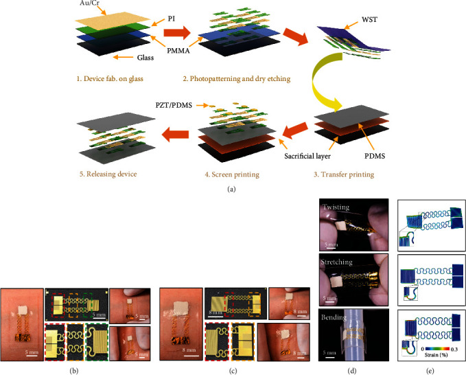
(a) Fabrication process flow of the intrinsically stretchable piezoelectric sensor for e-skin. (b, c) Photographs of two representative piezoelectric sensors with 5 × 5 mm2 (b) and 8 × 8 mm2 (c) sensing areas mounted onto a forearm; the enlarged images show the details of the electrode designs. (d, e) Images (d) and finite element modeling (e) of the device in bended, stretched, and twisted configurations.
Figure 2(a) shows the computered results of deformations in the sensor (top) and the Au layer (bottom) when pressure P = 30 kPa is applied to the working area. The maximum spacing among the electrodes increases by ~2.6% due to the stretched phantom skin induced by the applied pressure. Evaluation of the relationship between the voltage output of the sensor and the values of a set of stress that span those of tactile forces confirmed the linear response behavior of the senor to the external stress, as shown in Figure 2(b) and S5(a). Figure 2(b) and S5(a) present the peak voltage in 64 mm2 and 25 mm2 sensors as a function of various applied touched forces from 0.1 kPa to 110.4 kPa. The sensitivity of the sensors can be calculated from the fitted curve as 0.067 V/kPa for 64 mm2 devices and 0.01 V/kPa for 25 mm2 devices, respectively. Figure 2(c) shows the voltage versus time of the sensor with the applied stress of 87.5 kPa, where the device yields a peak voltage output of 5.2 V with great signal-to-noise ratio, indicating its high sensitivity and effective responsivity to external stimuli (Figure 2(c)). Figure 2(d), S6 and S7 show the electrical signal versus time with three different frequencies (1 Hz, 5 Hz, and 10 Hz) at a constant stress of 64 kPa. It is interesting that the voltage output increases with frequency, because the same load amplitude increases the amount of work performed by the external force [53]. Similar to the tendency observed in Figure S6, the open-circuit voltage output yielded by the 25 mm2 device reaches to the highest value as the frequency approaches to 10 Hz at a constant stress of 110.4 kPa, as shown in Figure S5(b). By analyzing its electrical response at a constant stress of 87.5 kPa with three different frequencies, the response time ranges from 0.45 ms to 0.72 ms, as shown in Figure S8. Figure 2(e) shows the output voltage peak of the device under multiple cycles (>4500) of pressing at 32.4 kPa and 10 Hz, where the voltage amplitude after thousands of cycles of pressing still maintain its initial values, proving the great stability and durability. Figure 2(f) shows the details of the electrical signal marked in Figure 2(e).
Figure 2.
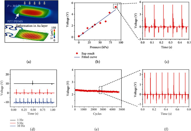
(a) The finite element analysis of a 5 × 5 mm2 device under a constant stress of 30 kPa onto its working area. (b) The electrical signal of the device versus applied stress at a constant frequency of 10 Hz. (c) Voltage output of the device as a function of time under stress of 87.5 kPa. (d) The electrical signal of the device versus time at a constant stress of 64 kPa under three different frequencies. (e) Peak values of each electrical output generated by the 64 mm2 device with over 4500 continuous working cycles under the load and frequency of 32.4 kPa and 10 Hz. (f) The details of the electrical signal in the marked region of (e).
Demonstration of e-skin testing involved in mounting the single-sensor device (64 mm2) on a volunteer's forearm and measuring the voltage responses to three types of typical tactile forces including touching, tapping, and hard pressing by a finger are shown in Figure 3(a). Due to the thin and soft features of the e-skin sensor, conformal contact without delamination from the skin was maintained during the entire measuring cycles of touching, tapping and hard pressing (Figure S9). Analysis of voltage outputs from the e-skin sensor stimulated by touching, tapping, and hard pressing is shown in Figure 3(b), where the device can accurately distinguish various tactile forces, with the pressure detection as low as 0.5 kPa (gentle touching). Intense force, i.e., finger hard pressing (10 kPa to 27.2 kPa) at a constant frequency of 2 Hz yields voltage outputs ranging from 0.63 V to 1.47 V, providing the sensor's self-powering capabilities (Figure 3(c)). To further investigate its electrical characteristics, a constant external trigger (hard finger pressing) was applied onto the device at four different stretching levels, including 0%, 2.8%, 8.3%, and 16.7%, as shown in Figure S10, and it is found that stretching the device has a negligible effect on its pressure sensing output. As shown in Figure S11, the uniform signal outputs, stimulated by hard finger pressing at three different locations of the 64 mm2 device, demonstrate its electrical anisotropy at the working area. Next, 10 small singe-unit sensors devices (working area, 25 mm2) were integrated onto different locations of latex gloves through van der Waals forces by a simple transfer method, which can provide information of voltage outputs for analyzing force distributions while grabbing an objective (Figures 3(d) and 3(e)). As shown in Figure 3(f), the voltage outputs of 10 sensors range from 14.1 mV to 113.8 mV when grabbing an empty cup. The sensor on the thumb (A1) yields the highest voltage output of ~113.8 mV on average and other sensors yield smaller voltage outputs of tens of mV. Such result clearly reveals the force distribution thereby proving the excellent performance and potentials for e-skin. Using the voltage outputs generated from finger motions, this enables the e-skin to act as an interface for human-machine integration. Various gestures of a robotic hand (uHand2.0, Shenzhen Hiwonder Co., Ltd.) with precise amplitudes and motions can be duplicated with a human hand while wearing the sensors in the latex gloves. As shown in Figures 3(g) and S12, the sensing voltage generated by the five individual sensors C1 to C5 are used to control the corresponding robotic fingers, including the thumb, forefinger, middle finger, ring finger, and little finger, through the Arduino board. Figure 3(g) shows a set of gestures, representing “Good,” “Okay,” and “Like you,” that translate to the hand by specific finger gestures and the corresponding voltage signals of these sensors are shown in Figure 3(h). With real-time data communication and algorithmic analysis, the robotic hand can identify and imitate the gestures of the human hand without time delay (Movie. S1).
Figure 3.
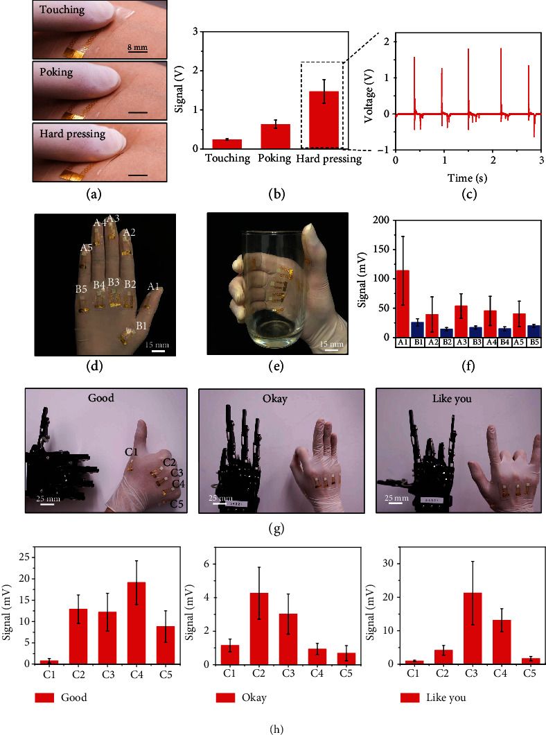
(a) Optical images illustrating three different external loads of touching (~0.5 kPa), poking (~13.4 kPa), and hard pressing (~27.2 kPa) on a piezoelectric elastomer sensor. (b, c) Electrical responses in the piezoelectric elastomer sensors to the three kinds of touching loads. (d) Optical image of a glove with 10 sensors mounted on different locations. (e) Photo of the sensors mounted on the glove grabbing a glass. (f) Electrical signals outputs of the 10 devices mounted on the glove when holding the glass. (g) Optical images of three gestures with 5 devices attached to the glove. (h) Voltage outputs of the 5 sensors mounted on the glove under gestures of “Good”, “Okay,” and “Like you”.
The first demonstration of the e-skin sensing array was investigated by using a stretchable sheet (70 mm × 45 mm) with 16 sensors arranged at 4 × 4, where the working area of each sensor is 64 mm2 (Figure 4(a)). This e-skin sensing array adopted the same device layout as the single-unit sensor (Figure S13). The ultrathin, soft PDMS substrate of the e-skin allows the device to conformally laminate onto the human skin through van der Waals forces without any irritation (Figure S14). The intrinsically stretchable nature of the piezoelectric sensors and advanced serpentine design of the metallic interconnects offer great flexibility and stretchability for skin integration. The device can still survive and maintain normal functions even after extreme mechanical force loadings, such as continuous stretching (~8%), twisting (~90°), and bending (180° at a radius of 3 mm) (Figure 4(b)). Figure S15 presents the electrical outputs of a 4 × 4 sensor array under the original state, bending for 100 and 200 cycles, and twisting for 100 and 200 cycles at a constant pressure and frequency of 10 kPa and 4 Hz. The unchanged signal outputs further prove the stability of the 4 × 4 sensor array. Figures 4(c)–4(e)show voltage responses in the sensing array for a representative touching pattern “CITYU” by a finger. It is clear that the e-skin is very sensitive to finger touching with obvious voltage output, affording the skin-like platform with capabilities to rebuild the tactile information.
Figure 4.

(a) Schematic illustration of an e-skin device with a 4 × 4 tactile sensor array. (b) Optical images of the device under three mechanical deformations, including stretching, twisting, and bending. (c–e) Characterizations of the e-skin device under a touching pattern of “CITYU” (c) and the voltage output distributions of 16 sensors (d, e).
Multiplexed device designs allow high-resolution and high-channel count e-skin interfaces by simplifying device geometry for tactile information acquisition (self-developed software, Figure S16). Here, the piezoelectric elastomer not only provides a great choice for sensors but also offers a scalable pathway towards large-area fabrication. A high sensing resolution embodiment with 100 channel sensors in a 2 cm × 2 cm area appears in Figure 5(a). This embodiment includes a 10 × 10 sensor array, contributing to a high density of 25 devices per square centimeter. A slightly difference from the layout of the aforementioned 16-channel device, an additional thin PI layer separates the conducting electrode and the interconnects for more compact integration. Selective area dry etching of this PI layer forms holes for connecting in-plane electrodes of the piezoelectric sensors and acquiring sensing data (Figure 5(b), S17). It is worth to mention the lot and functional piezoelectric sensor yields are both 100%, respectively, which can be attributed to the simple processing route used in this work. Figure 5(c) presents the optical images of a device mounted on the back hand and wrist of an examiner. More than a thousand bending and twisting cycles of the device did not affect the sensing performance, showing its robust mechanical properties (Figure 5(d)). Figure S18 summarizes the electrical signal outputs in the 10 × 10 sensor array tested under five mechanical deformations, including original state, bending for 100 and 200 cycles, and twisting for 100 and 200 cycles, at a constant pressure and frequency of 92.5 kPa and 4 Hz. Figure S19 presents the peak voltage by a unit of the 10 × 10 sensor array as a function of various applied touched forces from 12.9 kPa to 120 kPa with a sensitivity of 0.00018 V/kPa. The low sensitivity of the unit may mainly result from the middle PI layer, greatly impeding the strain level of the working area. Figure S20 shows the sensitivity of each unit of the 10 × 10 sensor array, ranging from 0.00016 V/kPa to 0.00019 V/kPa. Figure 5(e) summarizes the electrical responses of the device to various external triggers, including sliding in vertical and diagonal ways by a plastic rod (12.9 kPa), pressing by a metal bar (17.3 kPa), and a fingertip (~27.2 kPa). The spatial distribution of the amplitude of the evoked voltages measured by the e-skin sensing array is consistent with the tactile information, including the contact area and shape of the pressing objects as described with the color map (Figure 5(e)). Benefited from this platform, e-skin with the same materials and device architectures was also adapted to realize a larger area (4.2 cm × 4 cm) and 256 channel counts (16 × 16 sensor array) with a potential for applications that required large tactile sensing (Figure S21). To fabricate higher density of sensor arrays, decreasing the electrode width with resolution as high as several micrometer can be considered in the future.
Figure 5.

(a) Schematic illustration of the explosive view of an e-skin with a 10 × 10 tactile sensor array. (b) Optical images of the e-skin device and the enlarged photo of the electrode area. (c) Optical images of the device mounted onto the human skin. (d) Optical images of the device under two mechanical deformations of twisting and bending. (e) Voltage output distributions of the 10 × 10 sensors touched by different objects and different ways, including a plastic rod sliding along straight line and diagonal, a metal bar pressing, and finger touching.
3. Conclusion
In summary, we introduce a concept of increased channel counts e-skin with simple processing that build a foundation of the capabilities in skin-integrated device for accurate and high-resolution tactile sensing demonstrated by multiple hand motions/deformations and pressure sensing scenarios. By combining the advances in materials engineering, mechanic design and device integration, a high-throughput sensor with a large area and scalable e-skin was realized. The use of intrinsically stretchable piezoelectric elastomer sensors aligns with flexible electronics technology and offers potential applications in wearable technologies, health monitoring, and human-machine interfaces.
4. Materials and Methods
4.1. Fabrication of Piezoelectric Elastomer Composite
The piezoelectric elastomer sensors consist of PZT powders and PDMS, where the PZT powder (diameter of 0.9 μm on average) and PDMS (Sylgard 184) were purchased from Xi'an Yisheng electronics Co. Ltd., China, and Dow Corning Corporation. PZT (10 g), and PDMS (1.5 g, crosslink ratio of 10 : 1) was poured into a speed mixer and stirred at a speed of 500 rpm for 1 h to form elastomer precursors. Then, this mixture was transferred into an agate mortar and subsequently grinded for 1 h at room temperature. After full dispersion, the PZT/PDMS composite was poured into marked beakers for film casting.
4.2. Assembly of the Single and 4 × 4 Array Devices
The fabrication started on a quartz glass, which was first cleaned by acetone, alcohol, and deionized water (DI water) sequentially. A PMMA thin film was spin coated onto the glass at 2000 rpm (20 mg/ml) for 30 s and then baked on a hotplate at 200°C for 20 min, which served as the sacrificial layer. A thin layer of PI was spin coated on the PMMA (poly, amic acid solution 12.0 wt. % ±0.5 wt. %, 2 μm) at 3000 rpm for 30 s, baked at 250°C for 30 min. Next, Au/Cr (thickness, 200/40 nm; width, 50 μm) was sputtered onto the PI film and then patterned by photolithography and etching, yielding metal traces in the desired geometries. Here, a positive photoresist (PR, AZ 5214, AZ Electronic Materials) was spin coated at 3000 rpm for 30 s, soft bake on a hot plate at 110°C for 4 min, then exposed to ultraviolet light for 5 s, and finally developed for 15 s in a developer (AZ 300MIF). After developing, the PR was removed by acetone and rinsed with DI water. Then, we spin casted another layer of PI (2 μm, 3000 rpm for 30 s, annealed at 250°C for 30 min) and then selectively etched by Oxford Plasma-Therm 790 RIE system (patterns defined by photolithography similar as previous step) at the power of 200 W for 10 min, forming encapsulation layers for all interconnect areas besides the electrodes areas. Immersing the sample in acetone for 12 h dissolved the PMMA layer. Next, water-soluble tapes (WSTs) were used to pick up the patterns. We exposed the receiving PDMS substrates (PDMS: crosslink =30 : 1) and the WSTs to UV-induced ozone to create chemical groups between the electrodes and PDMS substrates to enhance the bonding strength. Attaching the WSTs on the PDMS and then heated in an oven at 70°C for 10 min formed strong bonding. Immersing the sample in water to remove the WSTs and realized soft stretchable electrodes. Next, piezoelectric elastomer precursors were screen-printed onto the stretchable electrodes via screen printing through a laser cut steel mask forming 0.3 mm thick sensors. After scree -printing the piezoelectric elastomer precursor, the sample was heated at 120°C for 30 min until the PZT elastomer was completely cured. Finally, the top PDMS (PDMS: crosslink =30 : 1) encapsulation layer with a thickness of 0.11 mm was spin coated and cured.
4.3. Assembly of the High-Channel Count Device
The fabrication started on a precleaned quartz glass. We attach a thin film of PI (thickness, 18 μm) on the glass supporting the substrate by a double-sided tape, then cleaned by ethanol. Next, Au/Cr (thickness, 200/40 nm; width, 500 μm) was sputtered onto the PI film and then patterned by photolithography and etching, yielding metal traces in the desired geometries (the same process and parameters as mentioned above). Then, we spin casted another layer of PI (2 μm) and then selective dry etching formed an encapsulation layer with small holes for connecting electrodes. We sputter another layer of Au/Cr (200 nm/40 nm) on the PI layer and then patterned by photolithography and etching, yielding an in-plane electrode. After releasing the sample from the glass sheet directly, we attach the sample onto a PDMS substrate. Next, the piezoelectric elastomer precursor was screen printed onto the electrodes via screen printing through a laser cut steel mask (thickness, 0.3 mm), followed by 120°C heating for 30 min until the piezoelectric elastomer was completely cured. Finally, the top PDMS encapsulation layer with a thickness of 0.11 mm was spin coated and cured.
4.4. Characterization
The piezoelectric charge constant (d33) of the PZT/PDMS elastomer was measured by YE2730A d33 meter. The voltage outputs of the single and 4 × 4 array devices were collected by a PL3516/P Powerlab 16/35 with a constant sampling frequency of 2 × 10⁴ Hz. The voltage output data of the high-channel count devices was collected by a NI PCI-6255 Data Acquisition Card. The elastic modulus of the PZT/PDMS composite was measured using a material testing machine (Lloyd LS1, AMETEK, USA) with an elongation speed of 50 mm/min at room temperature. The dimension of the composite is 50 × 10 mm. The external pressure was measured by a force sensor (NTJL-1, Nanjing Tianguang Electric Technology Co. Ltd.). The pressure by touching, tapping, and hard pressing are 0.5 kPa, 10 kPa, and 27.2 kPa, respectively.
4.5. Mechanical Simulations of the Stretchable Device
Finite element analysis (FEA) was implemented in ABAQUS (Analysis User's Manual 2016) to optimize the design layout to decrease the strain level in the Au/Cr layer for stretching, twisting, and bending skin deformations. The PDMS, PZT/PDMS composite, and phantom skin were modelled by hexahedron elements (C3D8R) while the thin Au/Cr layer (240 nm thick) and PI layers (2 μm) were modelled by shell elements (S4R). The minimal element size was 1/4 of the width of the Au/Gr wires (200 nm), which ensured the convergence and the accuracy of the simulation results. The d33 of the PZT/PDMS elastomer used in the analysis is 25 pC/N (measured d33 meter). The elastic modulus (E) and Poisson's ratio (ν) used in the analysis were EPDMS = 70 kPa, νPDMS = 0.5, EPI = 2.5 GPa, νPI = 0.34, EAu = 79 GPa, νAu = 0.4, ECr = 270 GPa, νCr = 0.21, EPZT/PDMS = 1 MPa, νPZT/PDMS = 0.46, ESkin = 130 kPa, and νSkin = 0.5.
Acknowledgments
This work was supported by the City University of Hong Kong (Grant Nos. 9610423, 9667199), Research Grants Council of the Hong Kong Special Administrative Region (Grant No. 21210820), and Department of Science and Technology of Sichuan Province (Grant No. 2020YFH0181). Z.X. acknowledges the support from the National Natural Science Foundation of China (Grant No. 12072057) and Fundamental Research Funds for the Central Universities (Grant No. DUT20RC(3)032).
Contributor Information
Lingqian Chang, Email: changlingqian1986@buaa.edu.cn.
Zuankai Wang, Email: zuanwang@cityu.edu.hk.
Xian Huang, Email: huangxian@tju.edu.cn.
Zhaoqian Xie, Email: zxie@dlut.edu.cn.
Zhengbao Yang, Email: zb.yang@cityu.edu.hk.
Xinge Yu, Email: xingeyu@cityu.edu.hk.
Conflicts of Interest
The authors declare that there is no conflict of interest regarding the publication of this article.
Authors' Contributions
X.G. Yu conceived the idea. Y. M. Liu designed, carried out the experiment, and wrote the paper. H. X. Zheng, S. Y. Liu, C. K. Yiu, and S. H. Gao assisted with experiment operations. L. Zhao analyzed the data. Z. Q. Xie and R. Avila conducted theoretical analysis of the device. Z. B. Yang, X. Huang, L. Q. Chang, and D. F. Li assisted with the scientific discussion of the article.
Supplementary Materials
Table S1: the summary of flexible piezoelectric pressure sensor based on sandwich and in-plane electrode design. Figure S1: the schematic diagram of the screen printing technology. Figure S2: the exploded-view schematic illustration of the single device with 25 mm2 working area. Figure S3: the electrical signals of the device (25 mm2 working area) versus (a) stress at a constant frequency of 10 Hz and (b) frequency at a constant stress of 110.4 kPa. Figure S4: the electrical signals of the 64 mm2 device versus frequency at a constant stress of 64 kPa. Figure S5: the electrical response of the 64 mm2 device under the constant stress of 64 kPa with three different frequencies. Figure S6: the enlarged electrical response of the 64 mm2 device at the constant stress of 87.5 kPa with three different frequencies. Figure S7: the optical images of the 64 mm2 device mounted onto the human skin under finger hitting. Figure S8: the electrical signal of the 64 mm2 device mounted onto the human skin with four different stretching levels under a constant stress and frequency of 27.2 kPa and 2 Hz. Figure S9: the electrical response of the 64 mm2 device mounted onto the human skin under a constant stress and frequency of 27.2 kPa and 2 Hz with the three different locations. Figure S10: (a) the schematic diagram of the testing circuit for controlling robotic hand. (b) The self-developed software interface for controlling the robotic hand. Figure S11: the exploded-view schematic diagram of the 4 × 4 array device. Figure S12: the optical images of the 4 × 4 array device mounted onto the forearm of an examiner. Figure S13: (a) the schematic diagram of the testing circuit for measuring the electrical signal of the multiplexed device. (b) The presence of the self-developed software interface as a finger is tapping on the multiplexed device. Figure S14: the enlarged optical image of the connection area between the 10 × 10 array device and ACF cables. Figure S15: the optical images of the 1616 array device.
Movie S1: Robotic hand controlling performed by the flexible e-skin.
References
- 1.Yu X., Xie Z., Yu Y., et al. Skin-integrated wireless haptic interfaces for virtual and augmented reality. Nature. 2019;575(7783):473–479. doi: 10.1038/s41586-019-1687-0. [DOI] [PubMed] [Google Scholar]
- 2.Yu X., Wang H., Ning X., et al. Needle-shaped ultrathin piezoelectric microsystem for guided tissue targeting via mechanical sensing. Nature Biomedical Engineering. 2018;2(3):165–172. doi: 10.1038/s41551-018-0201-6. [DOI] [PubMed] [Google Scholar]
- 3.Liu Y., Zhao L., Avila R., et al. Epidermal electronics for respiration monitoring via thermo-sensitive measuring. Materials Today Physics. 2020.
- 4.Tian L., Zimmerman B., Akhtar A., et al. Large-area MRI-compatible epidermal electronic interfaces for prosthetic control and cognitive monitoring. Nature Biomedical Engineering. 2019;3(3):194–205. doi: 10.1038/s41551-019-0347-x. [DOI] [PubMed] [Google Scholar]
- 5.Madhvapathy S. R., Ma Y., Patel M., et al. Epidermal electronic systems for measuring the thermal properties of human skin at depths of up to several millimeters. Advanced Functional Materials. 2018;28(34, article 1802083) doi: 10.1002/adfm.201802083. [DOI] [Google Scholar]
- 6.Wang S., Xu J., Wang W., et al. Skin electronics from scalable fabrication of an intrinsically stretchable transistor array. Nature. 2018;555(7694):83–88. doi: 10.1038/nature25494. [DOI] [PubMed] [Google Scholar]
- 7.Zhu C., Chortos A., Wang Y., et al. Stretchable temperature-sensing circuits with strain suppression based on carbon nanotube transistors. Nature Electronics. 2018;1(3):183–190. doi: 10.1038/s41928-018-0041-0. [DOI] [Google Scholar]
- 8.Jang K. I., Jung H. N., Lee J. W., et al. Ferromagnetic, folded electrode composite as a soft interface to the skin for long-term electrophysiological recording. Advanced Functional Materials. 2016;26(40):7281–7290. doi: 10.1002/adfm.201603146. [DOI] [PMC free article] [PubMed] [Google Scholar]
- 9.Yang Z., Zhou S., Zu J., Inman D. High-performance piezoelectric energy harvesters and their applications. Joule. 2018;2(4):642–697. doi: 10.1016/j.joule.2018.03.011. [DOI] [Google Scholar]
- 10.Ma Y., Choi J., Hourlier-Fargette A., et al. Relation between blood pressure and pulse wave velocity for human arteries. Proceedings of the National Academy of Sciences. 2018;115(44):11144–11149. doi: 10.1073/pnas.1814392115. [DOI] [PMC free article] [PubMed] [Google Scholar]
- 11.Kim B. H., Liu F., Yu Y., et al. Mechanically guided post-assembly of 3D electronic systems. Advanced Functional Materials. 2018;28(48, article 1803149) doi: 10.1002/adfm.201803149. [DOI] [Google Scholar]
- 12.Guo C. F., Ren Z. Flexible transparent conductors based on metal nanowire networks. Materials Today. 2015;18(3):143–154. doi: 10.1016/j.mattod.2014.08.018. [DOI] [Google Scholar]
- 13.Yi F., Wang X., Niu S., et al. A highly shape-adaptive, stretchable design based on conductive liquid for energy harvesting and self-powered biomechanical monitoring. Science advances. 2016;2(6, article e1501624) doi: 10.1126/sciadv.1501624. [DOI] [PMC free article] [PubMed] [Google Scholar]
- 14.Jang K. I., Li K., Chung H. U., et al. Self-assembled three dimensional network designs for soft electronics. Nature Communications. 2017;8(1):1–10. doi: 10.1038/ncomms15894. [DOI] [PMC free article] [PubMed] [Google Scholar]
- 15.Qiang Y., Seo K. J., Zhao X., et al. Bilayer nanomesh structures for transparent recording and stimulating microelectrodes. Advanced Functional Materials. 2017;27(48, article 1704117) doi: 10.1002/adfm.201704117. [DOI] [Google Scholar]
- 16.Ma Q., Cheng H., Jang K. I., et al. A nonlinear mechanics model of bio-inspired hierarchical lattice materials consisting of horseshoe microstructures. Journal of the Mechanics and Physics of Solids. 2016;90:179–202. doi: 10.1016/j.jmps.2016.02.012. [DOI] [PMC free article] [PubMed] [Google Scholar]
- 17.Ma Q., Zhang Y. Mechanics of fractal-inspired horseshoe microstructures for applications in stretchable electronics. Journal of Applied Mechanics. 2016;83(11) doi: 10.1115/1.4034458. [DOI] [Google Scholar]
- 18.Wang H., Ning X., Li H., et al. Vibration of mechanically-assembled 3D microstructures formed by compressive buckling. Journal of the Mechanics and Physics of Solids. 2018;112:187–208. doi: 10.1016/j.jmps.2017.12.002. [DOI] [PMC free article] [PubMed] [Google Scholar]
- 19.Liu Y., Zhao L., Wang L., et al. Skin-integrated graphene-embedded lead zirconate titanate rubber for energy harvesting and mechanical sensing. Advanced Materials Technologies. 2019;4(12, article 1900744) doi: 10.1002/admt.201900744. [DOI] [Google Scholar]
- 20.Liu Y., Wang L., Zhao L., et al. Thin, skin-integrated, stretchable triboelectric nanogenerators for tactile sensing. Advanced Electronic Materials. 2020;6(1, article 1901174) doi: 10.1002/aelm.201901174. [DOI] [Google Scholar]
- 21.Huang Y., Wang Y., Sun X., et al. Superelastic and large-range pressure sensor with hollow-sphere architectures for wearable electronic skin. Smart Materials and Structures. 2020;29(4, article 045014) doi: 10.1088/1361-665X/ab73e1. [DOI] [Google Scholar]
- 22.Yu J., Hou X., He J., et al. Ultra-flexible and high-sensitive triboelectric nanogenerator as electronic skin for self-powered human physiological signal monitoring. Nano Energy. 2020;69:p. 104437. doi: 10.1016/j.nanoen.2019.104437. [DOI] [Google Scholar]
- 23.Asghar W., Li F., Zhou Y., et al. Piezocapacitive flexible e-skin pressure sensors having magnetically grown microstructures. Advanced Materials Technologies. 2019;5(2, article 1900934) [Google Scholar]
- 24.Ren Z., Ding Y., Nie J., et al. Environmental energy harvesting adapting to different weather conditions and self-powered vapor sensor based on humidity-responsive triboelectric nanogenerators. ACS Applied Materials & Interfaces. 2019;11(6):6143–6153. doi: 10.1021/acsami.8b21477. [DOI] [PubMed] [Google Scholar]
- 25.Guo H., Lan C., Zhou Z., Sun P., Wei D., Li C. Transparent, flexible, and stretchable WS2based humidity sensors for electronic skin. Nanoscale. 2017;9(19):6246–6253. doi: 10.1039/C7NR01016H. [DOI] [PubMed] [Google Scholar]
- 26.Miao L., Wan J., Song Y., et al. Skin-inspired humidity and pressure sensor with a wrinkle-on-sponge structure. ACS Applied Materials & Interfaces. 2019;11(42):39219–39227. doi: 10.1021/acsami.9b13383. [DOI] [PubMed] [Google Scholar]
- 27.Jeong W., Song J., Bae J., Nandanapalli K. R., Lee S. Breathable nanomesh humidity sensor for real-time skin humidity monitoring. ACS Applied Materials & Interfaces. 2019;11(47):44758–44763. doi: 10.1021/acsami.9b17584. [DOI] [PubMed] [Google Scholar]
- 28.Ding Y., Shi Y., Nie J., et al. Thermochromic triboelectric nanogenerator enabling direct visualization of temperature change during operation. Chemical Engineering Journal. 2020;388:p. 124369. doi: 10.1016/j.cej.2020.124369. [DOI] [Google Scholar]
- 29.Lu C. X., Han C. B., Gu G. Q., et al. Temperature effect on performance of triboelectric nanogenerator. Advanced Engineering Materials. 2017;19(12):p. 1700275. doi: 10.1002/adem.201700275. [DOI] [Google Scholar]
- 30.Huang J., Xu Z., Qiu W., et al. Stretchable and heat-resistant protein-based electronic skin for human thermoregulation. Advanced Functional Materials. 2020;30(13):p. 1910547. doi: 10.1002/adfm.201910547. [DOI] [Google Scholar]
- 31.Cao Z., Yang Y., Zheng Y., et al. Highly flexible and sensitive temperature sensors based on Ti3C2Tx(MXene) for electronic skin. Journal of Materials Chemistry A. 2019;7(44):25314–25323. doi: 10.1039/C9TA09225K. [DOI] [Google Scholar]
- 32.Shin J., Jeong B., Kim J., et al. Sensitive wearable temperature sensor with seamless monolithic integration. Advanced Materials. 2019;32(2, article 1905527) doi: 10.1002/adma.201905527. [DOI] [PubMed] [Google Scholar]
- 33.Jiang Y., Liu M., Yan X., et al. Electrical breakdown-induced tunable piezoresistivity in graphene/polyimide nanocomposites for flexible force sensor applications. Advanced Materials Technologies. 2018;3(8, article 1800113) doi: 10.1002/admt.201800113. [DOI] [Google Scholar]
- 34.Lao S., Edher H., Saini U., Sixt J., Salehian A. A novel capacitance-based in-situ pressure sensor for wearable compression garments. Micromachines. 2019;10(11, article 743) doi: 10.3390/mi10110743. [DOI] [PMC free article] [PubMed] [Google Scholar]
- 35.Dai S., Wang S., Yan H., et al. Stretchable and self-healable hydrogel-based capacitance pressure and strain sensor for electronic skin systems. Materials Research Express. 2019;6(8, article 0850b9) doi: 10.1088/2053-1591/ab2320. [DOI] [Google Scholar]
- 36.Chen H., Miao L., Su Z., et al. Fingertip-inspired electronic skin based on triboelectric sliding sensing and porous piezoresistive pressure detection. Nano Energy. 2017;40:65–72. doi: 10.1016/j.nanoen.2017.08.001. [DOI] [Google Scholar]
- 37.Cheng X., Xue X., Ma Y., et al. Implantable and self-powered blood pressure monitoring based on a piezoelectric thinfilm: simulated, in vitro and in vivo studies. Nano Energy. 2016;22:453–460. doi: 10.1016/j.nanoen.2016.02.037. [DOI] [Google Scholar]
- 38.Li Q., Luo S., Wang Q.-M. Piezoresistive thin film pressure sensor based on carbon nanotube-polyimide nanocomposites. Sensors and Actuators A: Physical. 2019;295:336–342. doi: 10.1016/j.sna.2019.06.017. [DOI] [Google Scholar]
- 39.Yang Y., Zhang H., Lin Z. H., et al. Human skin based triboelectric nanogenerators for harvesting biomechanical energy and as self-powered active tactile sensor system. ACS Nano. 2013;7(10):9213–9222. doi: 10.1021/nn403838y. [DOI] [PubMed] [Google Scholar]
- 40.Pu X., Liu M., Chen X., et al. Ultrastretchable, transparent triboelectric nanogenerator as electronic skin for biomechanical energy harvesting and tactile sensing. Science advances. 2017;3(5, article e1700015) doi: 10.1126/sciadv.1700015. [DOI] [PMC free article] [PubMed] [Google Scholar]
- 41.Dagdeviren C., Joe P., Tuzman O. L., et al. Recent progress in flexible and stretchable piezoelectric devices for mechanical energy harvesting, sensing and actuation. Extreme Mechanics Letters. 2016;9:269–281. doi: 10.1016/j.eml.2016.05.015. [DOI] [Google Scholar]
- 42.Mahanty B., Maity K., Sarkar S., Mandal D. Human skin interactive self-powered piezoelectric e-skin based on PVDF/MWCNT electrospun nanofibers for non-invasive health care monitoring. Materials Today: Proceedings. 2020;21:1964–1968. [Google Scholar]
- 43.Gong S., Zhang B., Zhang J., Wang Z. L., Ren K. Biocompatible poly (lactic acid)-based hybrid piezoelectric and electret nanogenerator for electronic skin applications. Advanced Functional Materials. 2020;30(14, article 1908724) doi: 10.1002/adfm.201908724. [DOI] [Google Scholar]
- 44.Wu C., Kim T. W., Park J. H., et al. Self-powered tactile sensor with learning and memory. ACS nano. 2020;14(2):1390–1398. doi: 10.1021/acsnano.9b07165. [DOI] [PubMed] [Google Scholar]
- 45.Zhu X. X., Meng X. S., Kuang S. Y., et al. Triboelectrification-enabled touch sensing for self-powered position mapping and dynamic tracking by a flexible and area-scalable sensor array. Nano Energy. 2017;41:387–393. doi: 10.1016/j.nanoen.2017.09.025. [DOI] [Google Scholar]
- 46.Dagdeviren C., Shi Y., Joe P., et al. Conformal piezoelectric systems for clinical and experimental characterization of soft tissue biomechanics. Nature Materials. 2015;14(7):728–736. doi: 10.1038/nmat4289. [DOI] [PubMed] [Google Scholar]
- 47.Ning X., Yu X., Wang H., et al. Mechanically active materials in three-dimensional mesostructures. Science advances. 2018;4(9, article eaat8313) doi: 10.1126/sciadv.aat8313. [DOI] [PMC free article] [PubMed] [Google Scholar]
- 48.He J., Guo X., Yu J., et al. A high-resolution flexible sensor array based on PZT nanofibers. Nanotechnology. 2020;31(15, article 155503) doi: 10.1088/1361-6528/ab667a. [DOI] [PubMed] [Google Scholar]
- 49.Hosseini E. S., Manjakkal L., Shakthivel D., Dahiya R. Glycine–chitosan-based flexible biodegradable piezoelectric pressure sensor. ACS Applied Materials & Interfaces. 2020;12(8):9008–9016. doi: 10.1021/acsami.9b21052. [DOI] [PMC free article] [PubMed] [Google Scholar]
- 50.Jeong S.-I., Lee E. J., Hong G. R., et al. Three-dimensional multistack-printed, self-powered flexible pressure sensor arrays: piezoelectric composites with chemically anchored heterogeneous interfaces. ACS Omega. 2020;5(4):1956–1965. doi: 10.1021/acsomega.9b03753. [DOI] [PMC free article] [PubMed] [Google Scholar]
- 51.Yang Y., Pan H., Xie G., et al. Flexible piezoelectric pressure sensor based on polydopamine-modified BaTiO3/PVDF composite film for human motion monitoring. Sensors and Actuators A: Physical. 2020;301:p. 111789. doi: 10.1016/j.sna.2019.111789. [DOI] [Google Scholar]
- 52.Chen J., Liu H., Wang W., et al. High durable, biocompatible, and flexible piezoelectric pulse sensor using single-crystalline III-N thin film. Advanced Functional Materials. 2019;29(37, article 1903162) doi: 10.1002/adfm.201903162. [DOI] [Google Scholar]
- 53.Dagdeviren C., Yang B. D., Su Y., et al. Conformal piezoelectric energy harvesting and storage from motions of the heart, lung, and diaphragm. Proceedings of the National Academy of Sciences. 2014;111(5):1927–1932. doi: 10.1073/pnas.1317233111. [DOI] [PMC free article] [PubMed] [Google Scholar]
Associated Data
This section collects any data citations, data availability statements, or supplementary materials included in this article.
Supplementary Materials
Table S1: the summary of flexible piezoelectric pressure sensor based on sandwich and in-plane electrode design. Figure S1: the schematic diagram of the screen printing technology. Figure S2: the exploded-view schematic illustration of the single device with 25 mm2 working area. Figure S3: the electrical signals of the device (25 mm2 working area) versus (a) stress at a constant frequency of 10 Hz and (b) frequency at a constant stress of 110.4 kPa. Figure S4: the electrical signals of the 64 mm2 device versus frequency at a constant stress of 64 kPa. Figure S5: the electrical response of the 64 mm2 device under the constant stress of 64 kPa with three different frequencies. Figure S6: the enlarged electrical response of the 64 mm2 device at the constant stress of 87.5 kPa with three different frequencies. Figure S7: the optical images of the 64 mm2 device mounted onto the human skin under finger hitting. Figure S8: the electrical signal of the 64 mm2 device mounted onto the human skin with four different stretching levels under a constant stress and frequency of 27.2 kPa and 2 Hz. Figure S9: the electrical response of the 64 mm2 device mounted onto the human skin under a constant stress and frequency of 27.2 kPa and 2 Hz with the three different locations. Figure S10: (a) the schematic diagram of the testing circuit for controlling robotic hand. (b) The self-developed software interface for controlling the robotic hand. Figure S11: the exploded-view schematic diagram of the 4 × 4 array device. Figure S12: the optical images of the 4 × 4 array device mounted onto the forearm of an examiner. Figure S13: (a) the schematic diagram of the testing circuit for measuring the electrical signal of the multiplexed device. (b) The presence of the self-developed software interface as a finger is tapping on the multiplexed device. Figure S14: the enlarged optical image of the connection area between the 10 × 10 array device and ACF cables. Figure S15: the optical images of the 1616 array device.
Movie S1: Robotic hand controlling performed by the flexible e-skin.