Abstract
Over the past six years, researchers have investigated the use of spray coating to fabricate perovskite solar cells (PSCs), with the aim of demonstrating its viability as an industrial manufacturing process. This spotlight on applications outlines the key benefits of this coating technology and summarizes progress made to date, with attention focused on varied efforts to control the crystallization and uniformity of the perovskite layer. The emerging understanding of processes required to create smooth, dense spray-cast perovskite films has recently led to the demonstration of fully spray-cast PSCs with a power conversion efficiency of 19.4%.
Keywords: perovskite solar cells, spray coating, scalable fabrication, antisolvent, vacuum-assisted solution processing
Introduction
Perovskite solar cells are a relatively new class of photovoltaic device that utilizes ionic crystals having the perovskite structure ABX3 as their light-absorbing layer. When incorporated into devices, lead halide perovskites have demonstrated single-junction power conversion efficiencies (PCEs) as high as 25.2%.1 This excellent performance is attributed to their intrinsic semiconducting character, allowing for long electron and hole charge-carrier diffusion lengths,2,3 as well as efficient light absorption and low nonradiative recombination rates due to electronically benign bulk defects.4 Unlike other high efficiency photovoltaic materials such as silicon, perovskite films can be easily crystallized from solution at low temperature. This is a particularly attractive feature, as it enables devices to be fabricated quickly and at low cost, reducing the energy payback time by using common printing techniques.5 Furthermore, as the semiconductor band gap of a perovskite can be modified by adjusting the composition of the material,6 many believe that they will find near-term practical application in silicon-perovskite tandem devices that have efficiencies surpassing those of current single-junction silicon-based devices.7
Currently, most research developing perovskite materials uses spin coating, which involves the perovskite precursor solution being spread across a substrate via shear forces. This technique is simple and widely accessible, so it has been used to fabricate most high-efficiency devices reported in the literature. However, spin coating can suffer from poor process reproducibility between research laboratories. It is also poorly suited to coating large areas because of wasted solution lost from the substrate during coating and thickness nonuniformities generally introduced when scaling the coated area beyond a few square centimeters.8 As a result, a growing community of researchers are investigating alternative scalable deposition techniques to deposit perovskite PV devices from solution, including blade-coating,9 slot-die coating,10 inkjet printing,11 and spray coating.12
In this spotlight on applications, we discuss the use of spray coating to fabricate perovskite solar cells (PSCs). Rather than being a full review of the literature, attention is focused on the development of so-called “one-step” spray processes; however, we briefly introduce progress in the development of PSCs spray cast using a “two-step” methodology. As appropriate for a spotlight on applications, our discussion includes a particular focus on the progress and learning made within our research team at the University of Sheffield (U.K.).
Basic Principles of Perovskite Spray-Coating
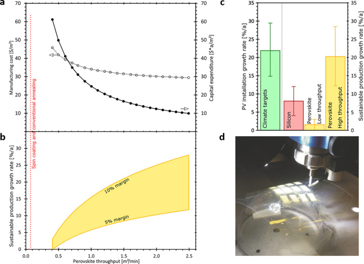
Spray-coating is a technique that we have investigated extensively to fabricate both organic13−16 and perovskite12,17−21 photovoltaic devices. In comparison with other scalable techniques, spray deposition has two advantages. First, spray coating is often significantly faster than other techniques as a spray head can move across a substrate at more than 5 m per minute, more than twice as fast as the typically reported speeds for slot-die coating.22 A cost model by Bruening et al.23 has shown the benefit for the significantly lower capital expenditure costs associated with a high-throughput perovskite photovoltaic module factory compared to an equivalent capacity silicon or cadmium telluride factory. As shown in Figure 1a, the effective annual cost per unit fabricated module area (expressed in units of $*a/m2, where “$*a” denotes annual costs) is critically dependent on the throughput speed of the continuous manufacturing process. Intuitively, the cost of a factory represents a fixed cost, with the production capacity largely dictating the operating margin (Figure 1b). A higher operating margin would therefore increase the funds available for reinvestment in growing production, which is critical to ensure sustainable growth of solar energy required to meet global energy demands, while concomitantly decarbonising energy production (Figure 1c). Perovskites have the potential for such low capital expenditure, high-throughput manufacture and with spray coating already achieving speeds of 5–10 m/min in literature,12 a 1 m wide coating width would already be far below the lowest cost estimates in this model.
Figure 1.
Unique advantages for spray coating. (a) Open circles, manufacturing cost for perovskite modules, and filled circles, capital expenditure on the perovskite module level. The red dashed line indicates throughput levels attainable by spin coating and conventional (nonrapid) thermal annealing. (b) Sustainable growth rate for the production of perovskite modules as a function of throughput, derived from part a, shown for operating margins of 5 and 10%. (c) Comparison of targeted annual PV installation growth rate to reach climate goals with sustainable production growth rates for silicon and perovskite PV. (d) Photograph of direct printing process of perovskite on a hemispherical surface during aerosol-jet operation. Parts a–c reproduced with permission from ref (23). Copyright Elsevier 2018. Part d reproduced with permission from ref (24). Copyright Wiley 2017.
An additional benefit is the unique applications made possible by spray deposition. For instance, because a spray head is not in close contact with the surface during deposition, spray coating allows for nonplanar surfaces to be coated, as depicted in Figure 1d.24−26 We believe that this advantage could potentially enable PSCs to be directly coated over a range of “structural” materials and surfaces. However, the use of spray coating is not without its challenges; indeed, without careful control over solution chemistry and spray conditions, it is easy to create poor-quality films.22
We classify an idealized single pass spray process into four distinct stages.17,22 (1) A solution is sheared into a mist of micrometer-sized droplets as the spray head moves over a surface. Traditionally, this is achieved by forcing a solution through a narrow aperture or nozzle. However, many groups now use more sophisticated ultrasonic coaters equipped with piezoelectric transducers to break up the solution to be spray cast into a uniform mist.27 There has also been success with electrospray coating for this atomization process, where an applied voltage creates an electrostatic force at an aperture to produce a jet of droplets.28−31 (2) The spray mist is then guided to a surface with the assistance of a shaping gas. (3) Once the droplets reach a surface, they undergo a process of coalescence, forming a uniform wet film.32 (4) The wet film dries as solvent evaporates, leaving behind a solid thin film. Control over the film drying process is crucial; if a solution dries too quickly, the solution droplets may not have time to coalesce and level to form a uniform layer. Conversely, if the drying time is too long, the wet film can easily undergo dewetting, leading to films with poor coverage or morphology.33 To create high-quality films, a complex parameter space must be optimized that includes surface temperature, solution flow rate, solvent choice, and spray-head height/speed.34
Perovskite spray deposition is further complicated by the necessity of controlling the crystallization of the perovskite film as the precursor solution dries.35 Indeed, if nucleation and crystal growth are not carefully managed during the crystalline intermediate and perovskite film formation processes, the perovskite is often characterized by a rough surface composed of large (≈ 100 μm) crystallites,17−20,36−38 which are detrimental to both PSC device performance and stability. When fabricating PSCs by spin coating, it is common practice to drip an antisolvent onto the wet perovskite film to rapidly displace the primary perovskite solvent (often DMF), creating a supersaturated film without the necessity for heat. This in turn results in homogeneous nucleation when the film is thermally annealed, precipitating the growth of a uniform, smooth perovskite layer.39
Early Developments
Spray coating was used as early as 2004 to fabricate hybrid organic–inorganic perovskite-like materials;40 however, the first use of spray-coated perovskites in solar cells was reported by our group (Barrows et al.) in 2014.17 The process developed was relatively simple; a solution comprising a 3:1 ratio of methylammonium iodide to lead chloride (dissolved in DMF) was spray cast in air using an ultrasonic spray coater to create p-type/intrinsic/n-type (p-i-n) (or “inverted architecture”) devices having the structure ITO/PEDOT:PSS/perovskite/PCBM/Ca/Al. Here, it was necessary to control the spray-head height above the substrate together with its relative lateral velocity to control the film thickness. Notably, rather little was done (apart from control of substrate temperature during deposition) to manage the crystallization of the perovskite film. As a result, although high surface coverage was achieved, the efficiency of the PSC devices was relatively low, with a champion cell having 11% PCE reported. Figure 2 shows the champion PCE for sprayed PSCs cited in this article over time. Here we categorize results by (i) perovskite composition and (ii) whether the perovskite was deposited in a so-called “one-step” or “two-step” process.
Figure 2.
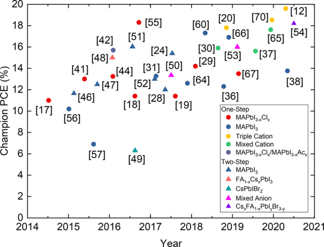
Progress in the champion power conversion efficiency of spray-coated perovskite solar cells over time. Circular data points are papers where the perovskite was deposited from a single solution (one-step). Triangular data points represent papers where the lead component and organic component were deposited separately, corresponding to a two-step process.
This work was then repeated and improved upon in 2015 by Das et al., who deposited the same perovskite in a similar manner to create n-i-p (or “normal architecture”) devices having the layer structure FTO/compact TiO2/perovskite/spiro-OMeTAD/Au.41 As a result of such a modification, the peak device PCE increased to 13%. The following, year Tait et al. further increased device efficiency by spray coating a blend of two perovskite solutions that were mixed in a spray head (3:1 MAI:PbCl2 and 3:1 MAI:PbAc).42 By varying the rate at which the solutions were delivered to the spray head, the final composition of the sprayed film could be varied. This method allowed a rapid compositional screening of the perovskite solutions, an approach that has been more recently applied to mixtures containing guanidinium, formamidinium, and cesium.43 By using a 3:1 blend of MAPbI3–xAcx to MAPbI3–xClx, Tait et al. were able to demonstrate PSC devices having a PCE of 15.7%.42 Another notable approach to improve film morphology using MAPbI3–xClx solutions was developed by Nejand et al., in which the authors used a cold-roll compressing technique to fabricate continuous perovskite films with densely packed grains.44 This novel approach to scalability using two DMF solvent-vapor recrystallization steps enabled devices with 13.2% PCE, although concerns remain regarding the stability of such solvent–vapor recrystallized films.45
Between 2015 and 2017, a series of papers were published using a two-step spray-assisted perovskite deposition process where the inorganic lead iodide layer was typically first spin coated before an organic solution was then sprayed onto the surface, with a reaction between the two components forming the perovskite.46−50 Although efficiencies as high as 15% have been demonstrated using this technique, the use of spin coating would still limit the overall scalability of the process.48 This issue was addressed in 2016 when Huang et al. sprayed both the PbI2 and MAI in a sequential two-step process, demonstrating a device with a PCE of 16.03%.51 Here, PbI2 was first spray cast from a DMSO solution, before a solution of MAI in IPA was sprayed onto the PbI2, with the formation of the perovskite facilitated by heating the substrate.
Although the use of one-step deposition techniques have been more often reported in the literature, recent years have demonstrated some impressive studies using a two-step deposition technique.52−54 Notably, Jiang et al. (2019) demonstrated the creation of solar mini-modules in which the lead iodide layer was first deposited by raster scanned ultrasonic spray coating (RUS), with the organic components (formamidinium iodide, formamidinium bromide, methylammonium chloride) being incorporated via chemical vapor deposition (CVD) to create a FAPbIxBr3–x perovskite.53 Here 12 cm2 modules were demonstrated with a PCE of 14.7%, an impressive efficiency for this device area. This process is shown schematically in Figure 3. A two-step process has also been adapted to deposit PbI2 nanocrystals suspended in IPA which were then reacted with spray-cast MAI in ethanol. This method has significant potential in the fabrication of perovskite layers in tandem devices and has the advantage that the solvents used are nontoxic.26
Figure 3.
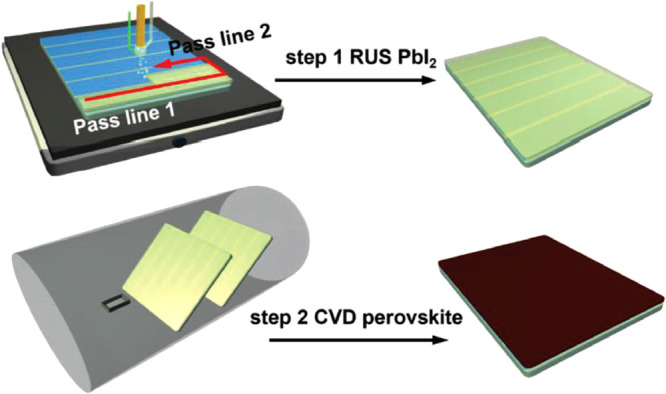
Perovskite film deposition using raster ultrasonic spray coating (RUS) combined with chemical vapor deposition (CVD) of the organic component. Schematic drawing of the RUS–CVD perovskite film deposition technology. PbI2 films are RUS coated on the FTO/c-TiO2 substrates, and converted to FAPbIxBr3–x via a CVD process. Reproduced with permission from ref (53). Copyright Wiley 2019.
In 2016, a new approach to the fabrication of spray-coated PSCs was outlined by Heo et al. Here CH3NH3PbI3 dissolved in DMF and GBL was continuously sprayed onto a substrate held at 120 °C.55 This unusual method of continuously soaking a surface, building on earlier layer-by-layer growth approaches,56,57 combined with the use of a novel solvent blend allowed perovskite grains to be partially redissolved and then regrown, with such grains reaching micrometer length scales. This allowed devices to be fabricated with a peak PCE of 18.3%, a record value that stood for several years, as well as 40 cm2 modules with 15.5% PCE. The interested reader is directed to our research perspective that discussed work on spray-coated PSCs published between 2014 and 2018.22
Following our first report on incorporating a spray-cast perovskite active layer in a PSC,17 we developed protocols to fabricate PSC devices in which all solution-processable layers in the device stack were spray cast. This was designed to demonstrate that spray casting could genuinely offer a route to the high-volume manufacturing of PSCs. In 2016, we reported a “fully spray-cast” PSC containing spray-cast PEDOT:PSS, MAPbI3-XClx and PCBM films, with champion devices reported having a PCE of 9.9%.18 The following year, we explored a different device architecture, based on spray-cast compact TiO2, mesoporous TiO2, MAPbI3–xClx, and spiro-OMeTAD, with devices created having a peak PCE of 10.2%.19
Although this work demonstrated the versatility of the ultrasonic spray-coating technique, it quickly became apparent that the morphology of the perovskite films that we were depositing was much rougher than those produced using conventional spin-coating processes that included an antisolvent quench. Indeed, the films that we had spray cast were often characterized by flower-shaped crystallites having a lateral size of hundreds of micrometers. In comparison, for the highest efficiency devices commonly reported in the literature, the perovskite layer comprised densely packed crystal grains that form highly specular films.58 Clearly, developing processes to more carefully control the crystallization of the perovskite from spray-coated layers was needed.
Antisolvent Bath Treatment
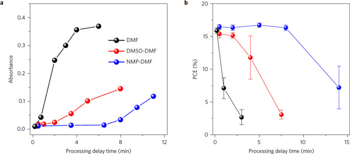
In 2017, Yang et al. published a study in which blade coating was used to deposit a MAPbI3 perovskite from a novel ink formulation comprising a 9:8 DMF:NMP solvent blend, producing devices having a PCE of 18.55%.59 Here, the lower volatility of NMP suppressed film drying, allowing the time window for antisolvent exposure to be extended. This allowed a wet film deposited via blade-coating to be dipped in a bath of diethyl ether to initiate controlled crystallization. Figure 4 shows the effect of the addition of the NMP solvent additive on crystallization rate. Figure 4a shows that the absorbance of the perovskite increased rapidly in the space of 2 min when the more-volatile DMF alone was used as the casting solvent. However, the crystallization was significantly retarded when the NMP was introduced, allowing an extended time window over which the antisolvent exposure could be used. Indeed, Figure 4b demonstrates that by using NMP in the solvent mixture, it is possible to delay the use of the antisolvent step by almost 10 min without compromising eventual device performance. In the same paper, Yang et al. also showed that the addition of MACl to the perovskite formulation enhanced both the size of the perovskite grains and their growth rate.
Figure 4.
(a) Average absorbance from 450 to 700 nm of perovskite precursor films as a function of the processing delay time between the precursor film being blade-coated and the antisolvent bath-exposure step. Three types of solvents were used: pure N,N-dimethylformamide (DMF), a mixture of dimethyl sulfoxide (DMSO) and DMF (9:8 v:v), and a mixture of N-methyl-2-pyrrolidinone (NMP) and DMF (9:8 v:v). (b) Impact of processing delay time on the power conversion efficiency (PCE) of devices fabricated using different solvents as indicated in part a. The device stack used was glass/fluorine-doped tin oxide (FTO)/compact TiO2 (c-TiO2)/perovskite/spiro-OMeTAD/Ag. Error bars represent standard deviations of 8–12 individual cells for each processing delay time. Reproduced with permission from ref (59). Copyright Springer Nature 2017.
In 2018, Uličná et al. adapted this approach and used an ultrasonic spray-based technique to deposit the same perovskite ink under ambient lab conditions.60 Here, the spray-cast wet film was dipped in diethyl ether for around 45 s until it changed color from yellow to brown. The coated substrate was then removed from the dipping bath and allowed to dry at ambient temperature, before being annealed at 150 °C for 90 s. Such films were incorporated into a standard architecture device having the structure FTO/SnO2/perovskite/spiro-OMeTAD/Au, with devices demonstrating a PCE of up to 17.3%. Crucially, when compared to a spin-coated control device, no significant change in efficiency was observed. In addition to such antisolvent baths, we also note work by Kim et al. in which an antisolvent was successfully spray coated during spin coating to create uniform films that were then fabricated into large-area devices.61 In more recent work, the same laboratory identified that a mixture of solvents is desirable for a more optimal sprayed antisolvent process,62 although this approach has not yet been combined with spray coating of the perovskite solution.
Vacuum-Assisted Solution Processing
Rather than use antisolvent exposure to initiate nucleation, previous work on spin-coated devices has shown brief exposure to a low vacuum63 is also able to rapidly extract DMF from a precursor film creating a supersaturated layer at room temperature, with thermal annealing being able to create a dense film of tightly packed crystallites. In 2018, we adopted this process (termed VASP, vacuum-assisted solution processing) as a post-treatment step for perovskite films deposited by spray coating under a N2 atmosphere.20
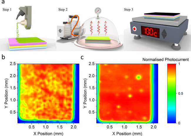
The VASP process is shown schematically in Figure 5a. First, a triple-cation (Cs0.05FA0.81MA0.14PbI2.55Br0.45) perovskite precursor was spray cast from an ultrasonic spray coater. Here, the spray-coating process occurred in a single pass of the spray head, with the spray pattern being wide enough to coat the whole substrate. By choosing a single-pass technique over multiple passes, we avoided creating additional parameters to optimize while keeping the deposition quick and simple. By holding the substrate at moderate temperature (40 °C), it was possible to enhance the wetting of the ink while not initiating crystallization of the wet film. In the next step, the substrate was transferred to a vacuum box for 5 min that was evacuated to 80 Pa using a rotary pump. This process initiated the crystallization of the perovskite film, creating a film that was brown in color. This film was then transferred to a hot plate and annealed under N2 to remove all remaining solvent and form the black perovskite phase. Using this method, devices were produced having a peak PCE of 17.8% (stabilized PCE of 17%), with such devices being the first example of a spray-coated triple-cation PSC.20
Figure 5.
(a) Schematic illustration of the spray deposition and VASP treatment process used to fabricate high-quality perovskite films. In step 1, the spray head moved across the surface depositing the precursor ink, which then created a wet film. In step 2, the wet film was exposed to a partial vacuum for 5 min to expel DMF from the film, forming a partially crystallized layer. In step 3, the crystallized intermediate film was annealed at 100 °C to form the perovskite phase. (b, c) Laser-beam-induced current (LBIC) maps of spray-cast perovskite devices. The perovskite film in part b was not exposed to vacuum, whereas that in part c was exposed to a low vacuum immediately after deposition. Reproduced with permission from ref (20). Copyright America Chemical Society 2018.
To understand the effect of the VASP step on the perovskite film morphology, we performed a series of characterization measurements to compare films to controls that were annealed immediately after the deposition of the wet film (i.e., without the VASP exposure step). Optically, it appeared that VASP-treated films were black and shiny (with a roughness (Ra) of ∼20 nm), whereas non-VASP films were rougher (Ra ≈ 100 nm) and appeared gray because of significant optical scattering.20 When imaged under a microscope, the non-VASP films were characterized by micrometer-sized flower-like crystallites similar to those observed in CH3NH3PbI3–xClx perovskite films spray cast in air.17−19 Unsurprisingly, when such films were incorporated into devices, the PCE of the devices fabricated without the VASP step had limited performance (PCE of ∼12% at best). This reduction in performance was characterized using laser-beam-induced current (LBIC) mapping. In this technique, a tightly focused laser spot is scanned across the device while the current is measured, allowing the photovoltaic response of the device to be imaged at micrometer length scales. This is shown in Figure 5b, where we plot an LBIC map of a non-VASP device, which shows the inhomogeneous photocurrent generation over the device area. In contrast, the device shown in Figure 5c in which the perovskite layer was VASP treated has significantly improved photocurrent uniformity.
Recent Developments
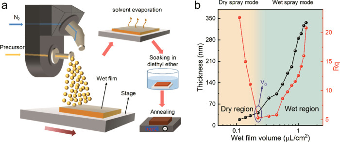
Between 2016 and 2020, a number of other groups published papers on spray-cast devices prepared using a variety of methods,64 including electrospray deposition,31,65 multiple spray passes,36 mixed-cation precursors,37 megasonic spray coating,66 hot air blowing,67 and colloidal quantum dots.68,69 Although none of these exceeded the record efficiency demonstrated by Heo et al. in 2016,55 the variety of deposition approaches demonstrated strengthened the case for the use of spray coating as a commercially viable technique. The next efficiency breakthrough came in late 2019, when Su et al. reported devices with a PCE of 18.53% by optimizing the work of Uličná.70 Here, the same solvent composition of NMP and DMF was used to spray cast devices, with the perovskite film subsequently dipped in a bath of diethyl ether antisolvent. This process is illustrated schematically in Figure 6a; here, the film was deposited in a single spray pass before being submerged in an antisolvent bath and then subsequently annealed. The principle innovation here was the use of a cesium containing triple-cation perovskite instead of MAPbI3, with MACl also added to the precursor solution to enhance grain growth. Using this process, devices were scaled up to an active area of 1 cm2, with devices fabricated on both rigid glass and flexible PET substrates. Such large devices demonstrated reverse scan PCE values of 15.07 and 13.21%, respectively, which are some of the highest values reported in the literature.70
Figure 6.
Sprayed film deposition mode. (a) Schematic illustration of single-pass spray-coated perovskite film in wet spray mode. (b) Thickness and roughness of perovskite films as a function of the volume of the sprayed precursor on the substrate. Here, V0 is the threshold between wet and dry spray modes. Reproduced with permission from ref (70). Copyright American Chemical Society 2019.
It has been shown that the successful use of an antisolvent exposure (or VASP) process requires the volume of the wet film deposited before treatment to be large enough to prevent uneven drying and crystallization.20,70 Wet film volume during spray coating can be effectively controlled by varying flow rate, head speed, and head height. Figure 6b shows the effect of varying the wet film volume on both film thickness and roughness of the resultant perovskite layer as reported by Su et al. Empirically, it was found that if the volume of the wet film was below a critical threshold (V0), then the solution would dry before exposure to the antisolvent, forming a thin but relatively rough film. However, by increasing the wet film volume above V0, the solution drying rate was reduced, allowing time for the wet film to level and the antisolvent treatment to be applied effectively. Here, the roughness of the treated film increases as a function thickness; however, it remains sufficiently low (20 nm Rq) for smooth perovskite layers to be created that are suitable for efficient light harvesting.
Recently, we used the VASP spray-deposition method to create fully sprayed devices. Our objective was to bring together the improved understanding of techniques used to create smooth, high-density perovskite films and develop a process in which all layers in a PSC could be deposited using a spray-based process. Here, the device architecture developed consisted of ITO/nanoparticle SnO2 (np-SnO2)/triple-cation perovskite/spiro-OMeTAD/gold. Preliminary experiments demonstrated that a np-SnO2 film can be spray coated from an aqueous np-SnO2 solution using an air-based spray coater in a single pass.21 The VASP TC perovskite deposition process was also further optimized for scalability with a significantly shorter vacuum exposure time used (1 min rather than 5 min), which resulted in a slight improvement in device performance.12 In addition, further efficiency gains were achieved by reducing the thickness of the spray-cast spiro-OMeTAD layer.
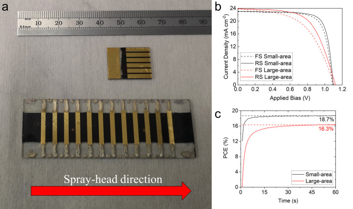
As a result of such optimization studies, we were able to fabricate fully spray-coated PSC devices having a PCE of 19.4%.12 We emphasize that these PCE values were obtained from small cells having an active area of 2.5 mm2. We also therefore performed a limited scale up of device area and fabricated a series of devices on 25 × 75 mm2 substrates. These ITO-coated substrates were patterned into 12 15.4 mm2 active area devices as shown in Figure 7a. The same figure shows a small area fully spray-cast device for comparison. Here champion all-spray “large-area” devices having an active area of 15.4 mm2 had a reverse scan PCE of 16.3%. It was also shown that by connecting seven devices in parallel on a single large-area substrate, it was possible to create a device having an effective active area of 1.08 cm2 with a PCE of 12.7%.12 For completeness, we plot JV data and stabilized power measurements for the champion fully sprayed devices on both the small and large-area substrates in Figure 7b, c, respectively.
Figure 7.
(a) Fully spray-cast perovskite solar cells on small and large-area substrates. (b) JV data from the champion fully sprayed small and large-area devices that had a reverse scan PCE of 19.4% and 16.3% respectively. (c) Output power of the champion devices when held (for 60 s) at a fixed voltage close to the maximum power point, indicating a stabilized PCE of 18.7 and 16.3% for small- and large-area cells, respectively. This image is adapted from ref (12) and licensed under CC BY-ND 2.0.
Although this work is an important step in the efficiency for fully spray-coated PSCs, we found that it was difficult to fully eliminate morphological defects in the film. Here, the main issue encountered was the formation of voids in the perovskite layer, which significantly reduced device performance.12 We believe that such voids result from the wet film undergoing partial dewetting around surface contaminants in the SnO2 layer during the VASP process. We expect that by further improving the SnO2 spray-coating process and developing the perovskite solvent chemistry, it will be possible to minimize these effects. This result, and the necessity for coating our highest efficiency devices in a N2 glovebox, strongly suggests that any industrial spray-coating technique must be performed under well-controlled clean-room conditions.
Conclusion
In summary, spray coating of perovskite photovoltaics is a research area that continues to grow, with continued efficiency gains expected in the coming years with both one- and two-step processes showing great promise. The scope for future experimentation and process development is significant, with areas set for investigation including new low volatility perovskite solution formulations, transport materials, and perovskite compositions with improved stability, together with improved post-treatment steps, interface passivation, and rapid crystallization methods. We note that a particularly promising alternative post-treatment step is the use of air blading, where a high-pressure gas jet is directed over a surface to accelerate solvent evaporation and supersaturation of the precursor film as required to create highly uniform thin films.71
Acknowledgments
This work was funded by the UK Engineering and Physical Sciences Research Council (EPSRC) via grant EP/S009213/1 “The integration of photovoltaic devices with carbon-fibre composites”. We also thank the EPSRC for funding PhD studentships via the Centre for Doctoral Training in New and Sustainable PV, EP/L01551X/1 (J.A.S.).
The authors declare the following competing financial interest(s): D.G.L. is co-director of the company Ossila Ltd. that sells materials and equipment for perovskite photovoltaic device research and development.
References
- NREL. Best Research-Cell Efficiency Chart. https://www.nrel.gov/pv/cell-efficiency.html (accessed July 2020).
- Stranks S. D.; Eperon G. E.; Grancini G.; Menelaou C.; Alcocer M. J. P.; Leijtens T.; Herz L. M.; Petrozza A.; Snaith H. J. Electron-Hole Diffusion Lengths Exceeding 1 Micrometer in an Organometal Trihalide Perovskite Absorber. Science 2013, 342, 341. 10.1126/science.1243982. [DOI] [PubMed] [Google Scholar]
- Herz L. M. Charge-Carrier Mobilities in Metal Halide Perovskites: Fundamental Mechanisms and Limits. ACS Energy Lett. 2017, 2 (7), 1539–1548. 10.1021/acsenergylett.7b00276. [DOI] [Google Scholar]
- Steirer K. X.; Schulz P.; Teeter G.; Stevanovic V.; Yang M.; Zhu K.; Berry J. J. Defect Tolerance in Methylammonium Lead Triiodide Perovskite. ACS Energy Lett. 2016, 1 (2), 360–366. 10.1021/acsenergylett.6b00196. [DOI] [Google Scholar]
- Gong J.; Darling S. B.; You F. Perovskite Photovoltaics: Life-Cycle Assessment of Energy and Environmental Impacts. Energy Environ. Sci. 2015, 8, 1953–1968. 10.1039/C5EE00615E. [DOI] [Google Scholar]
- Jesper Jacobsson T.; Correa-Baena J.-P.; Pazoki M.; Saliba M.; Schenk K.; Gratzel M.; Hagfeldt A. An Exploration of the Compositional Space for Mixed Lead Halogen Perovskites for High Efficiency Devices - SI. Energy Environ. Sci. 2016, 9 (5), 1706–1724. 10.1039/C6EE00030D. [DOI] [Google Scholar]
- Jošt M.; Kegelmann L.; Korte L.; Albrecht S. Monolithic Perovskite Tandem Solar Cells: A Review of the Present Status and Advanced Characterization Methods Toward 30% Efficiency. Adv. Energy Mater. 2020, 10 (26), 1904102. 10.1002/aenm.201904102. [DOI] [Google Scholar]
- Howard I. A.; Abzieher T.; Hossain I. M.; Eggers H.; Schackmar F.; Ternes S.; Richards B. S.; Lemmer U.; Paetzold U. W. Coated and Printed Perovskites for Photovoltaic Applications. Adv. Mater. 2019, 31 (26), 1806702. 10.1002/adma.201806702. [DOI] [PubMed] [Google Scholar]
- Wu W.-Q.; Wang Q.; Fang Y.; Shao Y.; Tang S.; Deng Y.; Lu H.; Liu Y.; Li T.; Yang Z.; Gruverman A.; Huang J. Molecular Doping Enabled Scalable Blading of Efficient Hole-Transport-Layer-Free Perovskite Solar Cells. Nat. Commun. 2018, 9 (1), 1625. 10.1038/s41467-018-04028-8. [DOI] [PMC free article] [PubMed] [Google Scholar]
- Whitaker J. B.; Kim D. H.; Larson B. W.; Zhang F.; Berry J. J.; Van Hest M. F. A. M.; Zhu K. Scalable Slot-Die Coating of High Performance Perovskite Solar Cells. Sustain. Energy Fuels 2018, 2 (11), 2442–2449. 10.1039/C8SE00368H. [DOI] [Google Scholar]
- Li P.; Liang C.; Bao B.; Li Y.; Hu X.; Wang Y.; Zhang Y.; Li F.; Shao G.; Song Y. Inkjet Manipulated Homogeneous Large Size Perovskite Grains for Efficient and Large-Area Perovskite Solar Cells. Nano Energy 2018, 46 (February), 203–211. 10.1016/j.nanoen.2018.01.049. [DOI] [Google Scholar]
- Bishop J. E.; Read C. D.; Smith J. A.; Routledge T. J.; Lidzey D. G. Fully Spray-Coated Triple-Cation Perovskite Solar Cells. Sci. Rep. 2020, 10 (1), 6610. 10.1038/s41598-020-63674-5. [DOI] [PMC free article] [PubMed] [Google Scholar]
- Wang T.; Scarratt N. W.; Yi H.; Dunbar A. D. F.; Pearson A. J.; Watters D. C.; Glen T. S.; Brook A. C.; Kingsley J.; Buckley A. R.; Skoda M. W. A.; Donald A. M.; Jones R. A. L.; Iraqi A.; Lidzey D. G. Fabricating High Performance, Donor-Acceptor Copolymer Solar Cells by Spray-Coating in Air. Adv. Energy Mater. 2013, 3 (4), 505–512. 10.1002/aenm.201200713. [DOI] [Google Scholar]
- Griffin J.; Pearson A. J.; Scarratt N. W.; Wang T.; Lidzey D. G.; Buckley A. R. Organic Photovoltaic Devices Incorporating a Molybdenum Oxide Hole-Extraction Layer Deposited by Spray-Coating from an Ammonium Molybdate Tetrahydrate Precursor. Org. Electron. 2014, 15 (3), 692–700. 10.1016/j.orgel.2013.12.028. [DOI] [Google Scholar]
- Zhang Y.; Griffin J.; Scarratt N. W.; Wang T.; Lidzey D. G. High Efficiency Arrays of Polymer Solar Cells Fabricated by Spray-coating in Air. Prog. Photovoltaics 2016, 24 (3), 275–282. 10.1002/pip.2665. [DOI] [Google Scholar]
- Griffin J.; Ryan A. J.; Lidzey D. G. Solution Modification of PEDOT:PSS Inks for Ultrasonic Spray Coating. Org. Electron. 2017, 41, 245–250. 10.1016/j.orgel.2016.11.011. [DOI] [Google Scholar]
- Barrows A.; Pearson A.; Kwak C.; Dunbar A.; Buckley A.; Lidzey D. Efficient Planar Heterojunction Mixed-Halide Perovskite Solar Cells Deposited via Spray-Deposition. Energy Environ. Sci. 2014, 7, 2944. 10.1039/C4EE01546K. [DOI] [Google Scholar]
- Mohamad D. K.; Griffin J.; Bracher C.; Barrows A. T.; Lidzey D. G. Spray-Cast Multilayer Organometal Perovskite Solar Cells Fabricated in Air. Adv. Energy Mater. 2016, 6, 1600994. 10.1002/aenm.201600994. [DOI] [Google Scholar]
- Bishop J. E.; Mohamad D. K.; Wong-Stringer M.; Smith A.; Lidzey D. G. Spray-Cast Multilayer Perovskite Solar Cells with an Active-Area of 1.5 Cm2. Sci. Rep. 2017, 7 (1), 7962. 10.1038/s41598-017-08642-2. [DOI] [PMC free article] [PubMed] [Google Scholar]
- Bishop J. E.; Smith J. A.; Greenland C.; Kumar V.; Vaenas N.; Game O. S.; Routledge T. J.; Wong-Stringer M.; Rodenburg C.; Lidzey D. G. High-Efficiency Spray-Coated Perovskite Solar Cells Utilizing Vacuum-Assisted Solution Processing. ACS Appl. Mater. Interfaces 2018, 10 (46), 39428–39434. 10.1021/acsami.8b14859. [DOI] [PubMed] [Google Scholar]
- Smith J. A.; Game O. S.; Bishop J. E.; Spooner E. L. K.; Kilbride R. C.; Greenland C.; Jayaprakash R.; Alanazi T. I.; Cassella E. J.; Tejada A.; Chistiakova G.; Wong-Stringer M.; Routledge T. J.; Parnell A. J.; Hammond D. B.; Lidzey D. G. Rapid Scalable Processing of Tin Oxide Transport Layers for Perovskite Solar Cells. ACS Appl. Energy Mater. 2020, 3, 5552. 10.1021/acsaem.0c00525. [DOI] [PMC free article] [PubMed] [Google Scholar]
- Bishop J. E.; Routledge T. J.; Lidzey D. G. Advances in Spray-Cast Perovskite Solar Cells. J. Phys. Chem. Lett. 2018, 9 (8), 1977–1984. 10.1021/acs.jpclett.8b00311. [DOI] [PubMed] [Google Scholar]
- Bruening K.; Dou B.; Simonaitis J.; Lin Y.-Y.; van Hest M. F. A. M.; Tassone C. J. Scalable Fabrication of Perovskite Solar Cells to Meet Climate Targets. Joule 2018, 2 (11), 2464–2476. 10.1016/j.joule.2018.09.014. [DOI] [Google Scholar]
- Bag S.; Deneault J. R.; Durstock M. F. Aerosol-Jet-Assisted Thin-Film Growth of CH 3 NH 3 PbI 3 Perovskites-A Means to Achieve High Quality, Defect-Free Films for Efficient Solar Cells. Adv. Energy Mater. 2017, 7 (20), 1701151. 10.1002/aenm.201701151. [DOI] [Google Scholar]
- Carey T.; Jones C.; Le Moal F.; Deganello D.; Torrisi F. Spray-Coating Thin Films on Three-Dimensional Surfaces for a Semitransparent Capacitive-Touch Device. ACS Appl. Mater. Interfaces 2018, 10 (23), 19948–19956. 10.1021/acsami.8b02784. [DOI] [PMC free article] [PubMed] [Google Scholar]
- Sansoni S.; De Bastiani M.; Aydin E.; Ugur E.; Isikgor F. H.; Al-Zahrani A.; Lamberti F.; Laquai F.; Meneghetti M.; De Wolf S. Eco-Friendly Spray Deposition of Perovskite Films on Macroscale Textured Surfaces. Adv. Mater. Technol. 2020, 5 (2), 1901009. 10.1002/admt.201901009. [DOI] [Google Scholar]
- Majumder M.; Rendall C.; Li M.; Behabtu N.; Eukel J. A.; Hauge R. H.; Schmidt H. K.; Pasquali M. Insights into the Physics of Spray Coating of SWNT Films. Chem. Eng. Sci. 2010, 65 (6), 2000–2008. 10.1016/j.ces.2009.11.042. [DOI] [Google Scholar]
- Kavadiya S.; Niedzwiedzki D. M.; Huang S.; Biswas P. Electrospray-Assisted Fabrication of Moisture-Resistant and Highly Stable Perovskite Solar Cells at Ambient Conditions. Adv. Energy Mater. 2017, 7 (18), 1700210. 10.1002/aenm.201700210. [DOI] [Google Scholar]
- Han S.; Kim H.; Lee S.; Kim C. Efficient Planar-Heterojunction Perovskite Solar Cells Fabricated by High-Throughput Sheath-Gas-Assisted Electrospray. ACS Appl. Mater. Interfaces 2018, 10 (8), 7281–7288. 10.1021/acsami.7b18643. [DOI] [PubMed] [Google Scholar]
- Jiang Y.; Wu C.; Li L.; Wang K.; Tao Z.; Gao F.; Cheng W.; Cheng J.; Zhao X.-Y.; Priya S.; Deng W. All Electrospray Printed Perovskite Solar Cells. Nano Energy 2018, 53 (A), 440–448. 10.1016/j.nanoen.2018.08.062. [DOI] [Google Scholar]
- Hong S. C.; Lee G.; Ha K.; Yoon J.; Ahn N.; Cho W.; Park M.; Choi M. Precise Morphology Control and Continuous Fabrication of Perovskite Solar Cells Using Droplet-Controllable Electrospray Coating System. ACS Appl. Mater. Interfaces 2017, 9 (9), 7879–7884. 10.1021/acsami.6b15095. [DOI] [PubMed] [Google Scholar]
- Brian D.; Ahmadian-Yazdi M.-R.; Barratt C.; Eslamian M. Impact Dynamics and Deposition of Perovskite Droplets on PEDOT:PSS and TiO2 Coated Glass Substrates. Exp. Therm. Fluid Sci. 2019, 105, 181–190. 10.1016/j.expthermflusci.2019.03.021. [DOI] [Google Scholar]
- Deegan R. D.; Bakajin O.; Dupont T. F.; Huber G.; Nagel S. R.; Witten T. A. Contact Line Deposits in an Evaporating Drop. Phys. Rev. E: Stat. Phys., Plasmas, Fluids, Relat. Interdiscip. Top. 2000, 62 (1), 756–765. 10.1103/PhysRevE.62.756. [DOI] [PubMed] [Google Scholar]
- Eslamian M. Spray-on Thin Film PV Solar Cells: Advances, Potentials and Challenges. Coatings 2014, 4 (1), 60–84. 10.3390/coatings4010060. [DOI] [Google Scholar]
- Lilliu S.; Griffin J.; Barrows A. T.; Alsari M.; Curzadd B.; Dane T. G.; Bikondoa O.; Macdonald J. E.; Lidzey D. G. Grain Rotation and Lattice Deformation during Perovskite Spray Coating and Annealing Probed in Situ by GI-WAXS. CrystEngComm 2016, 18, 5448–5455. 10.1039/C6CE00965D. [DOI] [Google Scholar]
- Chou L. H.; Wang X. F.; Osaka I.; Wu C. G.; Liu C. L. Scalable Ultrasonic Spray-Processing Technique for Manufacturing Large-Area CH 3 NH 3 PbI 3 Perovskite Solar Cells. ACS Appl. Mater. Interfaces 2018, 10 (44), 38042–38050. 10.1021/acsami.8b12463. [DOI] [PubMed] [Google Scholar]
- Chou Y.-S.; Chou L.-H.; Guo A.-Z.; Wang X.-F.; Osaka I.; Wu C.-G.; Liu C.-L. Ultrasonic Spray-Coated Mixed Cation Perovskite Films and Solar Cells. ACS Sustainable Chem. Eng. 2019, 7 (16), 14217–14224. 10.1021/acssuschemeng.9b03058. [DOI] [Google Scholar]
- Chou L.-H.; Yu Y.-T.; Wang X.-F.; Osaka I.; Wu C.-G.; Liu C.-L. Sequential Ultrasonic Spray-Coating Planar Three Layers for 1 Cm 2 Active Area Inverted Perovskite Solar Cells. Energy Technol. 2020, 8, 2000216. 10.1002/ente.202000216. [DOI] [Google Scholar]
- Paek S.; Schouwink P.; Athanasopoulou E. N.; Cho K. T.; Grancini G.; Lee Y.; Zhang Y.; Stellacci F.; Nazeeruddin M. K.; Gao P. From Nano- to Micrometer Scale: The Role of Antisolvent Treatment on High Performance Perovskite Solar Cells. Chem. Mater. 2017, 29 (8), 3490–3498. 10.1021/acs.chemmater.6b05353. [DOI] [Google Scholar]
- Cheng Z. Y.; Wang H. F.; Quan Z. W.; Lin C. K.; Lin J.; Han Y. C. Layered Organic–Inorganic Perovskite-Type Hybrid Materials Fabricated by Spray Pyrolysis Route. J. Cryst. Growth 2005, 285 (3), 352–357. 10.1016/j.jcrysgro.2005.08.031. [DOI] [Google Scholar]
- Das S.; Yang B.; Gu G.; Joshi P. C.; Ivanov I. N.; Rouleau C. M.; Aytug T.; Geohegan D. B.; Xiao K. High-Performance Flexible Perovskite Solar Cells by Using a Combination of Ultrasonic Spray-Coating and Low Thermal Budget Photonic Curing. ACS Photonics 2015, 2 (6), 680–686. 10.1021/acsphotonics.5b00119. [DOI] [Google Scholar]
- Tait J. G.; Manghooli S.; Qiu W.; Rakocevic L.; Kootstra L.; Jaysankar M.; Masse de la Huerta C. A.; Paetzold U. W.; Gehlhaar R.; Cheyns D.; Heremans P.; Poortmans J. Rapid Composition Screening for Perovskite Photovoltaics via Concurrently Pumped Ultrasonic Spray Coating. J. Mater. Chem. A 2016, 4 (10), 3792–3797. 10.1039/C6TA00739B. [DOI] [Google Scholar]
- Stoddard R. J.; Rajagopal A.; Palmer R. L.; Braly I. L.; Jen A. K. Y.; Hillhouse H. W. Enhancing Defect Tolerance and Phase Stability of High-Bandgap Perovskites via Guanidinium Alloying. ACS Energy Lett. 2018, 3 (6), 1261–1268. 10.1021/acsenergylett.8b00576. [DOI] [Google Scholar]
- Abdollahi Nejand B.; Gharibzadeh S.; Ahmadi V.; Shahverdi H. R. New Scalable Cold-Roll Pressing for Post-Treatment of Perovskite Microstructure in Perovskite Solar Cells. J. Phys. Chem. C 2016, 120 (5), 2520–2528. 10.1021/acs.jpcc.5b11596. [DOI] [Google Scholar]
- Game O. S.; Smith J. A.; Alanazi T. I.; Wong-Stringer M.; Kumar V.; Rodenburg C.; Terrill N. J.; Lidzey D. G. Solvent Vapour Annealing of Methylammonium Lead Halide Perovskite: What’s the Catch?. J. Mater. Chem. A 2020, 8 (21), 10943–10956. 10.1039/D0TA03023F. [DOI] [Google Scholar]
- Boopathi K. M.; Ramesh M.; Perumal P.; Huang Y. C.; Tsao C. S.; Chen Y. F.; Lee C. H.; Chu C. W. Preparation of Metal Halide Perovskite Solar Cells through a Liquid Droplet Assisted Method. J. Mater. Chem. A 2015, 3 (17), 9257–9263. 10.1039/C4TA06392A. [DOI] [Google Scholar]
- Li F.; Bao C.; Gao H.; Zhu W.; Yu T.; Yang J.; Fu G.; Zhou X.; Zou Z. A Facile Spray-Assisted Fabrication of Homogenous Flat CH3NH3PbI3 Films for High Performance Mesostructure Perovskite Solar Cells. Mater. Lett. 2015, 157, 38–41. 10.1016/j.matlet.2015.05.106. [DOI] [Google Scholar]
- Xia X.; Wu W.; Li H.; Zheng B.; Xue Y.; Xu J.; Zhang D.; Gao C.; Liu X. Spray Reaction Prepared FA 1–x Cs x PbI 3 Solid Solution as a Light Harvester for Perovskite Solar Cells with Improved Humidity Stability. RSC Adv. 2016, 6 (18), 14792–14798. 10.1039/C5RA23359C. [DOI] [Google Scholar]
- Lau C. F. J.; Deng X.; Ma Q.; Zheng J.; Yun J. S.; Green M. A.; Huang S.; Ho-Baillie A. W. Y. CsPbIBr 2 Perovskite Solar Cell by Spray-Assisted Deposition. ACS Energy Lett. 2016, 1 (3), 573–577. 10.1021/acsenergylett.6b00341. [DOI] [Google Scholar]
- Chai G.; Luo S.; Zhou H.; Daoud W. A. CH 3 NH 3 PbI 3–x Br x Perovskite Solar Cells via Spray Assisted Two-Step Deposition: Impact of Bromide on Stability and Cell Performance. Mater. Des. 2017, 125, 222–229. 10.1016/j.matdes.2017.04.010. [DOI] [Google Scholar]
- Huang H.; Shi J.; Zhu L.; Li D.; Luo Y.; Meng Q. Two-Step Ultrasonic Spray Deposition of CH3NH3PbI3 for Efficient and Large-Area Perovskite Solar Cell. Nano Energy 2016, 27, 352–358. 10.1016/j.nanoen.2016.07.026. [DOI] [Google Scholar]
- Remeika M.; Raga S. R.; Zhang S.; Qi Y. Transferrable Optimization of Spray-Coated PbI 2 Films for Perovskite Solar Cell Fabrication. J. Mater. Chem. A 2017, 5 (12), 5709–5718. 10.1039/C6TA09922J. [DOI] [Google Scholar]
- Jiang Y.; Remeika M.; Hu Z.; Juarez-Perez E. J.; Qiu L.; Liu Z.; Kim T.; Ono L. K.; Son D.; Hawash Z.; Leyden M. R.; Wu Z.; Meng L.; Hu J.; Qi Y. Negligible-Pb-Waste and Upscalable Perovskite Deposition Technology for High-Operational-Stability Perovskite Solar Modules. Adv. Energy Mater. 2019, 9 (13), 1803047. 10.1002/aenm.201803047. [DOI] [Google Scholar]
- Yu X.; Yan X.; Xiao J.; Ku Z.; Zhong J.; Li W.; Huang F.; Peng Y.; Cheng Y.-B. Interface Modification Effect on the Performance of Cs x FA 1–x PbI y Br 3–y Perovskite Solar Cells Fabricated by Evaporation/Spray-Coating Method. J. Chem. Phys. 2020, 153 (1), 014706 10.1063/5.0012803. [DOI] [PubMed] [Google Scholar]
- Heo J. H.; Lee M.; Jang M. H.; Im S. H. Highly Efficient CH3NH3PbI3-XClx Mixed Halide Perovskite Solar Cells Prepared by Re-Dissolution and Crystal Grain Growth via Spray Coating. J. Mater. Chem. A 2016, 4, 17636. 10.1039/C6TA06718B. [DOI] [Google Scholar]
- Ramesh M.; Boopathi K. M.; Huang T.; Huang Y.; Tsao C.; Chu C. Using an Airbrush Pen for Layer-by-Layer Growth of Continuous Perovskite Thin Films for Hybrid Solar Cells. ACS Appl. Mater. Interfaces 2015, 7 (4), 2359–2366. 10.1021/am506886d. [DOI] [PubMed] [Google Scholar]
- Gamliel S.; Dymshits A.; Aharon S.; Terkieltaub E.; Etgar L. Micrometer Sized Perovskite Crystals in Planar Hole Conductor Free Solar Cells. J. Phys. Chem. C 2015, 119 (34), 19722–19728. 10.1021/acs.jpcc.5b07554. [DOI] [Google Scholar]
- Noel N. K.; Habisreutinger S. N.; Wenger B.; Klug M. T.; Hörantner M. T.; Johnston M. B.; Nicholas R. J.; Moore D. T.; Snaith H. A Low Viscosity, Low Boiling Point, Clean Solvent System for the Rapid Crystallisation of Highly Specular Perovskite Films. Energy Environ. Sci. 2017, 10, 145. 10.1039/C6EE02373H. [DOI] [Google Scholar]
- Yang M.; Li Z.; Reese M. O.; Reid O. G.; Kim D. H.; Siol S.; Klein T. R.; Yan Y.; Berry J. J.; van Hest M. F. A. M.; Zhu K. Perovskite Ink with Wide Processing Window for Scalable High-Efficiency Solar Cells. Nat. Energy 2017, 2 (5), 17038. 10.1038/nenergy.2017.38. [DOI] [Google Scholar]
- Uličná S.; Dou B.; Kim D. H.; Zhu K.; Walls J. M.; Bowers J. W.; van Hest M. F. A. M. Scalable Deposition of High-Efficiency Perovskite Solar Cells by Spray-Coating. ACS Appl. Energy Mater. 2018, 1 (5), 1853–1857. 10.1021/acsaem.8b00328. [DOI] [Google Scholar]
- Kim J.; Yun J. S.; Cho Y.; Lee D. S.; Wilkinson B.; Soufiani A. M.; Deng X.; Zheng J.; Shi A.; Lim S.; Chen S.; Hameiri Z.; Zhang M.; Lau C. F. J.; Huang S.; Green M. A.; Ho-Baillie A. W. Y. Overcoming the Challenges of Large-Area High-Efficiency Perovskite Solar Cells. ACS Energy Lett. 2017, 2 (9), 1978–1984. 10.1021/acsenergylett.7b00573. [DOI] [Google Scholar]
- Lee D. S.; Bing J.; Kim J.; Green M. A.; Huang S.; Ho-Baillie A. W. Y. Grain Quality Engineering for Organic Metal Halide Perovskites Using Mixed Antisolvent Spraying Treatment. Sol. RRL 2020, 4 (1), 1900397. 10.1002/solr.201900397. [DOI] [Google Scholar]
- Li X.; Bi D.; Yi C.; Decoppet J.-D.; Luo J.; Zakeeruddin S. M.; Hagfeldt A.; Gratzel M. A Vacuum Flash-Assisted Solution Process for High-Efficiency Large-Area Perovskite Solar Cells. Science 2016, 353 (6294), 58–62. 10.1126/science.aaf8060. [DOI] [PubMed] [Google Scholar]
- Yao J.; Yang L.; Cai F.; Yan Y.; Gurney R. S.; Liu D.; Wang T. The Impacts of PbI 2 Purity on the Morphology and Device Performance of One-Step Spray-Coated Planar Heterojunction Perovskite Solar Cells. Sustain. Energy Fuels 2018, 2 (2), 436–443. 10.1039/C7SE00536A. [DOI] [Google Scholar]
- Heo J. H.; Im K.; Kim J.; Im S. H. Efficient Metal Halide Perovskite Solar Cells Prepared by Reproducible Electrospray Coating on Vertically Aligned TiO 2 Nanorod Electrodes. ACS Appl. Mater. Interfaces 2020, 12 (1), 886–892. 10.1021/acsami.9b19121. [DOI] [PubMed] [Google Scholar]
- Park M.; Cho W.; Lee G.; Hong S. C.; Kim M.-c.; Yoon J.; Ahn N.; Choi M. Highly Reproducible Large-Area Perovskite Solar Cell Fabrication via Continuous Megasonic Spray Coating of CH3NH3PbI3. Small 2019, 15 (1), 1804005. 10.1002/smll.201804005. [DOI] [PubMed] [Google Scholar]
- Su J.; Cai H.; Ye X.; Zhou X.; Yang J.; Wang D.; Ni J.; Li J.; Zhang J. Efficient Perovskite Solar Cells Prepared by Hot Air Blowing to Ultrasonic Spraying in Ambient Air. ACS Appl. Mater. Interfaces 2019, 11 (11), 10689–10696. 10.1021/acsami.9b01843. [DOI] [PubMed] [Google Scholar]
- Yuan J.; Bi C.; Wang S.; Guo R.; Shen T.; Zhang L.; Tian J. Spray-Coated Colloidal Perovskite Quantum Dot Films for Highly Efficient Solar Cells. Adv. Funct. Mater. 2019, 29 (49), 1906615. 10.1002/adfm.201906615. [DOI] [Google Scholar]
- Yang Z.; Wang M.; Li J.; Dou J.; Qiu H.; Shao J. Spray-Coated CsPbBr3Quantum Dot Films for Perovskite Photodiodes. ACS Appl. Mater. Interfaces 2018, 10 (31), 26387–26395. 10.1021/acsami.8b07334. [DOI] [PubMed] [Google Scholar]
- Su J.; Cai H.; Yang J.; Ye X.; Han R.; Ni J.; Li J.; Zhang J. Perovskite Ink with an Ultrawide Processing Window for Efficient and Scalable Perovskite Solar Cells in Ambient Air. ACS Appl. Mater. Interfaces 2020, 12 (3), 3531–3538. 10.1021/acsami.9b17141. [DOI] [PubMed] [Google Scholar]
- Ding J.; Han Q.; Ge Q. Q.; Xue D. J.; Ma J. Y.; Zhao B. Y.; Chen Y. X.; Liu J.; Mitzi D. B.; Hu J. S. Fully Air-Bladed High-Efficiency Perovskite Photovoltaics. Joule 2019, 3 (2), 402–416. 10.1016/j.joule.2018.10.025. [DOI] [Google Scholar]


