

A layer-engineered exfoliation approach allows us to obtain millimeter-size graphene and control the number of layers.
Abstract
The competition between quality and productivity has been a major issue for large-scale applications of two-dimensional materials (2DMs). Until now, the top-down mechanical cleavage method has guaranteed pure perfect 2DMs, but it has been considered a poor option in terms of manufacturing. Here, we present a layer-engineered exfoliation technique for graphene that not only allows us to obtain large-size graphene, up to a millimeter size, but also allows selective thickness control. A thin metal film evaporated on graphite induces tensile stress such that spalling occurs, resulting in exfoliation of graphene, where the number of exfoliated layers is adjusted by using different metal films. Detailed spectroscopy and electron transport measurement analysis greatly support our proposed spalling mechanism and fine quality of exfoliated graphene. Our layer-engineered exfoliation technique can pave the way for the development of a manufacturing-scale process for graphene and other 2DMs in electronics and optoelectronics.
INTRODUCTION
Since monolayer graphene was first successfully separated from three-dimensional (3D) natural graphite by top-down mechanical exfoliation (1), graphene with its unique physical and chemical properties has attracted great attention as an appealing platform for diverse applications in the fields of electronics, optoelectronics, and other fields (2–4). Nevertheless, mechanically exfoliated graphene still has limitations in terms of size, yield, and thickness control, which is not suitable for industrialization, resulting in a strong demand for alternative synthetic approaches. As an alternative method for preparing graphene, the vapor-deposition method has been considered to be one of the representative bottom-up methods for overcoming the aforementioned limitations of top-down mechanical exfoliation (5–7). However, because the inherent properties of graphene change substantially with the number of layers and stacking order (8, 9), the development of growth methods related to their control has been attempted (10, 11), but no outstanding results have yet been reported. Above all, the preexisting physical and chemical results obtained with exfoliated graphene are still far from being reproduced by as-grown graphene. Therefore, if a technique can overcome the issues of conventional mechanical exfoliation, then it will be the most attractive synthetic approach for preparing graphene.
Meanwhile, recent studies have revealed that exfoliation of 2D materials (2DMs) with the help of thin metal films can be key to obtaining scalable thin 2DM layers. To date, large-area monolayers of transition metal dichalcogenides (TMDCs) have been obtained by different exfoliation approaches, e.g., direct exfoliation on Au substrates (12, 13), the layer-resolved splitting technique by controlled crack propagation (14), and layer-by-layer exfoliation (15). Those studies were successful in obtaining large-area TMDCs but were limited to obtaining only monolayer TMDCs. Why only the topmost layer is peeled off is not yet sufficiently understood, hence limiting the application of the large-area exfoliation technique for various 2DMs, such as graphene, and the thickness control of exfoliated crystals.
In this study, we introduce the technique layer-engineered exfoliation (LEE) that not only guarantees large-area graphene but also provides control of the selective number of graphene layers owing to the difference in the interfacial binding energy between the used metal and graphene. A thin Au film is deposited on precleaved fresh graphite to selectively peel off the topmost graphene monolayer, as its interfacial toughness with graphene is similar to the interlayer binding energy of graphite. By adjusting the interfacial toughness through the deposition of different metal films (Pd, Ni, and Co) that have higher interfacial toughness than the Au film, large-area graphene with a controlled number of layers is also obtained. The exfoliated graphene does not exhibit any intrinsic defects or chemical contamination, as confirmed by spectroscopy and electron transport studies. We believe that our exfoliation method can be a promising approach for building large-area 2D heterostructures, revisiting the conventional exfoliation method that has been considered far from commercialization.
RESULTS AND DISCUSSION
LEE of graphene
As depicted in the schematic in Fig. 1A, to exfoliate large-area graphene with a selective number of layers, we directly evaporated a selective metal film onto a bulk graphite flake precleaved on the blue tape. The metal film was thermally evaporated up to 60 nm as a stressor on the graphite flake, where the tensile stress is given by the difference in the lattice constants of the graphite and metal films (16). By exfoliating the graphite flake with spin-coated poly(methyl methacrylate) (PMMA) and thermal release tape (TRT) as a handling layer, the external bending moment creates a crack at domain boundaries within the graphite flake initiated by tensile stress, and then, the crack propagates parallel to the metal-graphene interface, resulting in large-area exfoliation due to the residual tension (14). Such spalling of the top graphene layers occurs along the out-of-plane direction up to the spalling depth, which depends on the difference between the binding energy (γmetal-Gr) and interlayer binding energy of graphite (γGr-Gr), as shown in the inset of Fig. 1A (14, 17, 18). The higher the difference is, the deeper the spalling depth (experimental details will be discussed later, in relation to Fig. 2). After the transfer of exfoliated flakes onto a 300-nm SiO2/Si substrate, the TRT is removed, and the PMMA and metal film are subsequently chemically etched (see Materials and Methods for the detailed LEE process).
Fig. 1. LEE of millimeter-size monolayer graphene.
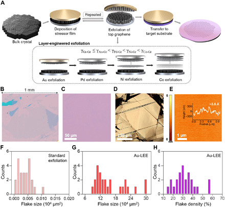
(A) Schematic illustration of our layer-engineered large-area graphene exfoliation technique. The inset shows the change in the number of layers of exfoliated graphene according to the relative binding energy between graphite and a metal stressor film. (B and C) Low- and high-magnification OM images of millimeter-size monolayer graphene obtained by the LEE method. (D and E) OM and AFM images of the cleaved natural graphite surface. The inset is a single trace of the AFM image showing the roughness of LEE-graphene, where the root mean square value is approximately 3.5 Å. (F to H) Histograms of the size and density of monolayer graphene obtained by the standard exfoliation and LEE methods for 25 samples each.
Fig. 2. Spalling depth control by adjusting the interfacial toughness.
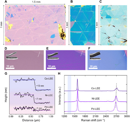
(A to C) Low-magnification and (D to F) high-magnification OM images of layer-engineered millimeter-size graphene prepared using Pd, Ni, and Co, respectively, on 300-nm SiO2/Si substrates. (G) AFM line profiles corresponding to the white dashed lines in (D) to (F). (H) Raman spectra of layer-engineered multilayer graphene obtained using Pd, Ni, and Co. a.u., arbitrary units.
Figure 1B shows a typical example of exfoliated monolayer graphene obtained by following the described LEE procedure, where a Au film was used as a stressor. The small difference in binding energy between Au-graphene (γAu-Gr = 30 meV/atom) (19) and graphene-graphene (γGr-Gr = 21–25 meV/atom) (20, 21) enables separation of a monolayer. The monolayer graphene we exfoliated typically shows a lateral size of a millimeter without physical defects inside it (Fig. 1, B and C), which is believed to be the largest exfoliated monolayer graphene ever reported (22). Here, the size of the exfoliated graphene is determined by that of the atomically flat domains of the mother graphite. Figure 1D illustrates the lateral size of individual domains of natural graphite with atomic-level flatness. This size is approximately a few hundred micrometers, similar to the size of the obtained monolayer graphene (Fig. 1, D and E, and figs. S1 and S2). However, there are still extra areas where empty layers or multilayers are present because not only the small binding energy difference tends to peel off solely the Au film without graphene (23) but also natural graphite is still bumpy at the millimeter scale, respectively (fig. S3). Our complementary experiment on highly oriented pyrolytic graphite (HOPG) confirms that the flat domain size matters, as the surface of HOPG exhibits many atomic steps that naturally occur during mechanical cleavage, leading to the large-scale and nonuniform monolayer graphene flake (fig. S4).
First, we quantitatively analyze the typical size and density of exfoliated monolayer graphene to verify the reliability of our LEE method for 25 samples (figs. S1 and S5). The average area of monolayer graphene obtained by the LEE method reaches 163,238 (±12,515) μm2, which is an increase of ~4200 times that of monolayer graphene exfoliated by the standard method, which yields 39 (±4.8) μm2 (Fig. 1, F and G). Our LEE method also shows better results than standard mechanical exfoliation in terms of the density of the monolayer. When calculating the area occupied by monolayer graphene in an arbitrary region (1 mm2 area) on the substrate, the density of the monolayer is measured to be only 0.0096% for the standard exfoliation method (fig. S6). However, as noted in Fig. 1H, the LEE method leads to a monolayer coverage of 34% (± 2.5) and up to 58% at some points. The reproducibility of the size and density of monolayer graphene ensures that this approach is a reliable method of exfoliating monolayer graphene in a controlled manner.
Then, to verify how robust our method is in obtaining large-area layer-engineered graphene by adjusting the spalling depth, we deposited various metal films as a selective stressor on graphite flakes. Each Pd, Ni, and Co film was evaporated on prepeeled graphite due to the higher binding energy with graphite than that of the Au film, where γPd-Gr = 84 meV/atom, γNi-Gr = 125 meV/atom, and γCo-Gr = 160 meV/atom (19). When natural graphite is exfoliated using the Pd film, bilayer graphene is observed in a 1.5 mm by 1 mm region of the 300-nm SiO2/Si substrate (Fig. 2A). Exfoliation with the Ni and Co films also results in uniform multilayer graphene with a lateral size of several hundred micrometers (Fig. 2, B and C). The high-resolution optical microscopy (OM) images shown in Fig. 2 (D to F) clearly indicate that the optical contrast of multilayer graphene changes from light purple to blue with increasing γmetal-Gr, as expected for thicker graphene layers. Atomic force microscopy (AFM) analysis along the dashed lines in Fig. 2 (D to F) confirms that exfoliation with the Pd, Ni, and Co film reproducibly results in bilayer, 8-nm-thick multilayer, and 20-nm-thick multilayer graphene (Fig. 2G). Raman spectroscopy analysis of the frequency and shape of the 2D peaks also supports the robustness of our LEE method, as shown in Fig. 2H. Exfoliated graphene obtained with the help of the Pd film shows the standard behavior of the 2D mode of bilayer graphene. Upon increasing the number of layers, multiple peaks appear in the 2D mode, and the center frequency is shifted to higher values, as indicated by the dashed line in Fig. 2H (24). All these data indicate that the number of exfoliated graphene layers increases with the use of Au to Co films as a stressor on graphite (fig. S7).
Spectroscopy analysis of LEE of graphene
Raman spectroscopy measurements on LEE of graphene (LEE-graphene) support our proposed spalling mechanism, as this technique is sensitive to the stress introduced during the spalling of graphene layers. Figure 3A shows the Raman spectra of LEE monolayer graphene, where G and 2D peaks are clearly observed. The G and 2D peaks in the Raman spectrum provide information on the applied strain in graphene. However, in the case of G peak analysis, extracting meaningful information by using the full width at half maximum (FWHM) of the G peak (ΓG) in the absence of a magnetic field is difficult because the FWHM strongly depends on the external environment, such as charge carrier doping, screening, or electronic broadening (25, 26). As expected, the FWHM of the 2D peak (Γ2D) does not depend on that of the G peak (ΓG), as shown in Fig. 3B. However, we can extract the important information as follows. Compared with the Γ2D of monolayer graphene exfoliated by the standard mechanical method and encapsulated by two hexagonal boron nitrides (hBNs; for details, see Materials and Methods; fig. S8), the Γ2D of LEE monolayer graphene is larger. According to Γ2D broadening, we assume that an amount of inhomogeneous strain is introduced during the Au-assisted LEE (Au-LEE) process. The value of Γ2D, however, is likely affected by charge doping, so we focused on the correlation between the frequencies of the G and 2D peak positions (ωG and ω2D, respectively) by using a simple vector model as represented in the inset of Fig. 3C and fig. S9 (27). This model consists of two vectors: OP = aeT + beH, where a and b are constants and eT and eH are unit vector components for tensile strain and hole doping effects, respectively. Here, the initial slope values of eT = 2.2 and eH = 0.7 were used (for details, see note S1). In addition, we set the origin, O (1582 and 2677 cm−1), as the intrinsic property of pristine graphene, where the intrinsic frequencies of the G and 2D peaks are not affected by extra charge and strain (27). As the strain and charge doping vary, ωG and ω2D move from O along eT and eH, respectively. In contrast, Q4 (Q1) is contributed by tensile (compressive) strain combined with the charge doping effect (Q2 and Q3 are not allowed because charge doping should result in an increase in ωG). On the basis of the relationship between the frequencies of the G (ωG) and 2D (ω2D) peaks, LEE-graphene shows a clear linear relationship with a slope of 2.2 (±0.1). This value is in good agreement with previous experimental and theoretical results under uniaxial (2.02 to 2.44) or biaxial (2.25 to 2.8) stress (27–29). Although our experimental results are in better agreement with the uniaxial-strain situation, the presence of biaxial strain or a mix of both cannot be excluded. All Raman points are located in Q4, which indicates that tensile strain is applied to LEE-graphene. When graphene is encapsulated by hBN crystals, Γ2D is decreased to ~23 (±2) cm−1 and (ωG and ω2D) moves to near the origin O (ω0G and ω02D), as shown in Fig. 3C. The results specify that tensile strain during the LEE process is released when graphene is lifted (detached) using hBN crystals, recovering the pristine property of normally exfoliated graphene.
Fig. 3. Characterization of monolayer graphene obtained by LEE.
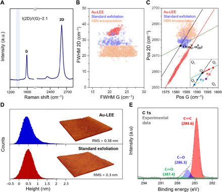
(A) Raman spectra of LEE-graphene under 532-nm excitation. (B and C) Γ2D versus ΓG and ω2D versus ωG recorded on three different samples: prepared by Au-LEE (red circles), standard exfoliation (blue circles), and hBN encapsulation (orange circles). (D) Surface roughness of monolayer graphene obtained by LEE and standard exfoliation scanned over 9 μm2. The insets show the corresponding 3D AFM images. Brown-to-yellow scale, 0 to 5 nm. (E) X-ray photoemission spectroscopy (XPS) patterns (C 1s) obtained from LEE-graphene. RMS, root mean square roughness.
Further microscopy and spectroscopy analysis also confirm the quality of our LEE-graphene. The absence of the disorder-related D peak near 1350 cm−1 (box colored in blue in Fig. 3A) and the symmetric Lorentzian line shape of the 2D peak in Fig. 3A indicate that the monolayer graphene obtained by Au-LEE is of high quality (fig. S10). The AFM measurements indicate that there are no notable physical defects, such as cracks, folding, and tearing, on the graphene surface (Fig. 3D). The root mean square roughness of LEE monolayer graphene is almost similar to that of normally exfoliated graphene on a silicon substrate (~0.8 Å difference), which is mostly due to the nonflat surface of the SiO2/Si substrate (30). In addition, considering that monolayer graphene acquired by Au-LEE is exposed to a chemical-based process to remove the TRT, including Au/PMMA layers, we confirmed that no critical chemical contaminants, such as PMMA and metal etchant residues, remain via x-ray photoelectron spectroscopy (XPS; Fig. 3E and fig. S11). The XPS spectrum shows a sharp C 1s peak and is fitted by three dominant Lorentzian modes that originate from typical sp2-hybridized carbon: C═C (284.6 eV), C─O (286.3 eV), and C═O (287.4 eV). Once a long chemical chain of PMMA is exposed to graphene, it is easily adsorbed on its surface, leading to indelible polymer residues (31). We verified that the intensity of amorphous carbon is negligible and that the intensity of its related peaks is very weak. Thus, we believe that the metal film effectively protects the surface of graphene from organic residues during the whole LEE process (16, 32).
Electron transport properties in LEE-graphene
To cross-check the quality of the LEE-graphene evidenced by the Raman spectroscopy and XPS results, we carried out electron transport measurements on the monolayer graphene device. Our graphene was encapsulated between defect-free hBN crystals (33), and then, the mesa was prepared by a sequential e-beam process, as shown in the inset of Fig. 4A (see Materials and Methods for the detailed hBN encapsulation and device fabrication process). Here, the encapsulation of graphene enables us to investigate the quality of the electron transport characteristics in the monolayer graphene that we prepared. hBN provides a flat and clean substrate for graphene, screens the charge fluctuations in the silicon substrate, and protects against contamination after exfoliation (33, 34). Figure 4A shows the back gate–dependent longitudinal resistivity ρ at temperature T = 2 K, measured by using a four-terminal configuration with the standard lock-in technique; a schematic of the wiring is shown in Fig. 4A. Here, the position of the charge-neutral point (CNP) is at the back-gate voltage Vbg = 1.5 V (corresponding to carrier density n = 9.0 × 1010 cm−2), which suggests that only negligible charged impurities and strain exist that can result in the shift of the CNP position (35). Next, to extract the level of the potential fluctuation n*, we plot the longitudinal conductivity σ as a function of n on a log scale (36). As shown in Fig. 4B, log(σ) remains constant when the electron transport is dominated by the potential fluctuation arising from charged impurities, whereas it shows a linear dependence on log(n) at high n. The crossing point of each extrapolated log(σ) dashed line in Fig. 4B provides the n* of our graphene device, which is essentially the same as that from an adequate exfoliated graphene device (34, 37) encapsulated between hBN. This again demonstrates the acceptable quality of our graphene device, although the graphene was in contact with the metal film during the transfer. We also determined the mobility μ (= σn−1e−1) of the device at T = 2 and 300 K to evaluate the quality of the device, where e is the electron charge (Fig. 4C). The mobility at 300 K is higher than 20,000 cm2 V−1 s−1, which is higher than the reported mobility of exfoliated graphene (38) on a silicon substrate but the same order of magnitude as that of the reported decent-quality graphene device (33) where the graphene was exfoliated by the standard method. The mobility at 2 K is approximately double that at 300 K due to the decreased momentum relaxation rate at low temperature. We also found a well-developed quantum Hall effect (Fig. 4D) in which the Landau levels start to split from ~1 T at low n and the degeneracy of the Landau levels is lifted at high magnetic fields, showing filling factors of −1, −2, −4, and −6, which we expect for high-quality graphene devices (39). The observations here therefore let us conclude that our LEE technique essentially does not degrade the quality of the graphene.
Fig. 4. Transport characteristics of hBN-encapsulated LEE-graphene.
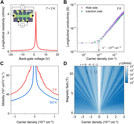
(A) Longitudinal resistivity as a function of back-gate voltage at 2 K (the CNP is at 1.5 V). The left inset shows an optical micrograph of the device with a wiring schematic for current and voltage measurements. Scale bar, 5 μm. (B) Density dependence of the longitudinal conductivity on a log scale at 2 K. The value of n* extracted from our graphene device is ~1010 cm−2. (C) Electron mobility as a function of carrier density at 2 K (red line) and 300 K (blue line). The mobility is approximately 20,000 cm2V−1 s−1 at 300 K. (D) Map of the longitudinal resistivity as a function of the applied magnetic field and carrier density at 2 K. The well-developed Landau levels indicate that the graphene device is of high quality (black dashed lines indicate filling factors of −1, −2, −4, and −6).
Conclusions
In summary, the LEE approach demonstrated here provides extraordinarily large-size and high-density graphene from natural graphite. In particular, by using different metal depositions that simply control the spalling depth, layer-engineered graphene can be obtained on a large scale. Unlike the standard exfoliation method that only allows a single peeling process, large-area graphene has been obtained several times from the same graphite flake by repeating the deposition and tearing process of the metal film (see Materials and Methods for the detailed repeated exfoliation process; fig. S12). Moreover, we applied the LEE approach to hBN, confirming that the number of layers of exfoliated hBN was also controlled by the selection of stressor films (fig. S13). We believe our results demonstrate that layer-engineered graphene can be exfoliated in a large area, paving the way for the development of a manufacturing-scale process for future applications based on 2D heterostructure.
MATERIALS AND METHODS
LEE process
First, bulk natural graphite (NGS Trading & Consulting, Gra-bluck) were stuck and cleaved on adhesive blue tape (ELP BT-150E-KL). Subsequently, the selected metal thin films were deposited on the graphite crystals by using an E-beam evaporation system. To avoid physical damage of graphene, we reduced the deposition rate to as low as 0.1 Å/s for 5 nm. The internal stress of metal film (σmetal) is estimated by using the Stoney formula, and the equation is given by , where R is the measured curvature of metal, R0 is the measured curvature of the substrate wafer, Ys is the Young’s modulus of the substrate, νs is the Poisson’s ratio of the substrate, ts is the thickness of the substrate, and t is the thickness of metal (16). The measured stress levels of each metal (Au, Pd, Ni, and Co) ranged from 300 to 450 MPa. Then, PMMA was spin-coated at 1500 rpm for 1 min. One hundred–micrometer-thick TRT (Revalpha 3196, Nitto Denko, TRT) is attached to the top of PMMA/metal/graphite as a handling layer. At this time, the PMMA layer is used to enhance conformal contact between the thin metal film and TRT. By applying gentle force, TRT/PMMA/metal/graphene was delaminated from bulk graphite and transferred onto 300-nm SiO2/Si substrates. The TRT lost its adhesion at 110°C. PMMA and metal film is completely removed by dipping it into acetone and appropriate metal etchant (Au etchant: product no. 651818, Sigma-Aldrich; Pd, Ni, and Co etchant: product no. 034256, Transene). To clean up the residues of the meal etchant on the graphene, we soaked the LEE-graphene in a flowing deionized water bath over 20 min (fig. S14).
hBN encapsulation and device fabrication
To measure the intrinsic properties of LEE-graphene, hBN-encapsulated graphene samples were prepared. Monolayer graphene was exfoliated by our LEE method as described above, and hBN flakes were obtained by the standard exfoliation method. We selected flat and clean hBN flakes. To pick up and drop our samples, we used the polydimethylsiloxane (PDMS)/poly(propylene) carbonate (PPC) template described in (40). First, the PDMS/PPC template was put in contact with the top hBN flake on 300-nm SiO2/Si and lifted up at 60°C. Subsequently, we attached the PDMS/PPC/hBN to LEE-graphene and raised the substrate temperature to above 130°C to improve the adhesion between graphene and hBN. After a few minutes, only the PDMS was lifted, and the top hBN remained on the LEE-graphene. In the same manner, after that, we picked up the top hBN/graphene at 60°C and dropped it onto the bottom hBN at 130°C using the PDMS/PPC template, assembling an hBN-encapsulated graphene structure. The Hall bar structure was patterned by standard e-beam lithography (width: 2.0 μm; length: 3.0 μm). Reactive ion etching in SF6/Ar plasma [40 standard cubic centimeters per minute (sccm)/40 sccm, 100 W, 1 min] was applied to expose the graphene edge (33). Subsequently, Cr/Au metal films (5 nm/45 nm) were deposited by thermal evaporation and lifted off in acetone, resulting in a 1D-edge metal contact.
Calculation of the density and area of exfoliated monolayer graphene
To calculate the size and density of exfoliated monolayer graphene on 300-nm SiO2/Si substrates, we used the open-source image processing program ImageJ (https://imagej.net) (41). After obtaining OM images of arbitrary regions (1 mm by 1 mm) where graphene flakes were exfoliated, whole pixels of images were extracted. Subsequently, the contrast value (C) of each pixel was calculated by the following equation: C = (CR + CG + CB)/3, where CR, CG, and CB are the R, G, and B values per pixel in the color image, respectively. Using the above equation, we obtained the optical contrast of monolayer graphene (CML) and the substrate (CS) from the optical image in fig. S5. The contrast difference (CD; same as CS − CML) between monolayer graphene and the 300-nm SiO2/Si substrate was calculated to be −4.7 (fig. S5D). Then, regions with the same CD values were selected from the original image, and the number of selected pixels was calculated (fig. S5, A to C). The density of monolayer graphene was calculated by dividing the number of pixels of the selected monolayer graphene by the total number of pixels. The area was calculated by selecting individual graphene domains in the form of a simple closed curve selected by the ImageJ program (fig. S5E).
Repeated exfoliation process
Unlike the typical exfoliation method in which only a single peeling process is feasible, large-area monolayers have been obtained several times from the same graphite flake by repeating the deposition and tearing process of the Au film. Three repeated exfoliations were carried out for the same domain, and each process result is shown in fig. S12. Monolayer graphene with a lateral size of ~300 μm was obtained during the first, second, and third repeated exfoliations. The area of the obtained monolayer was calculated to be ~80,000 μm2 for the first graphene monolayer. For the same flake position, the areas of the second and third graphene monolayers were ~74,000 and ~78,000 μm2. The quality of the repeatedly exfoliated monolayer graphene was confirmed by Raman analysis. The intensity ratios of the 2D peak and G peak, I2D/IG, of the first, second, and third exfoliated graphene were approximately 1.9, 2.0, and 2.1, respectively. In addition, no D peak was observed in each spectrum, indicating that the physical and chemical defect levels of the monolayer graphene are low and that the crystallinity is high.
Characterization
Surface morphology and thickness analysis was conducted by OM (Nikkon) and NX10 AFM (Park Systems Corp.) under tapping mode at a slow scanning rate (~0.3 Hz). Raman measurements were performed using a WITec Raman system [excitation wavelength of 2.33 eV (532 nm)] with a piezo stage, which was used to obtain large-area mapping data. The laser power was less than 1 mW to avoid laser-induced heating of the 2D materials. The Si peak at 520 cm−1 was used as a reference for wave number calibration. All the peaks of the acquired Raman spectra were fitted by Lorentzian. XPS analysis was performed to characterize the surface chemical state of graphene. It was carried out using an ESCA2000 spectrometer with monochromatic Al Kα radiation (1468.6 eV). The peak energies were calibrated using the C 1s peak at 284.6 eV.
Supplementary Material
Acknowledgments
Funding: This work was supported by the National Research Foundation of Korea (grant nos. 2020R1A4A4079397 and 2019R1G1A1100363), POSCO Science Fellowship of POSCO TJ Park Foundation, and Samsung Display Co. Ltd. K.W. and T.T. acknowledge support from the Elemental Strategy Initiative conducted by the MEXT, Japan, grant no. JPMXP0112101001, JSPS KAKENHI grant no. JP20H00354, and the CREST (JPMJCR15F3), JST. Author contributions: J.-Y.M., D.W., S.-K.S., and J.-H.L. conceived the idea for this research project. J.-Y.M. and S.-I.K. performed the LEE of graphene, conducted characterizations, and data analyses. M.K., S.X., and S.-K.S. made graphene devices and conducted transport measurements. M.K., J.-H.C., and S.-K.S. carried out the Raman analysis. D.S.P., J.S., and S.H.C. participated in graphene and hBN exfoliation and data analyses. K.W. and T.T. grew high-quality hBN single crystals. J.-Y.M., M.K., S.-K.S., and J.-H.L. wrote the manuscript. S.-K.S. and J.-H.L. supervised the research. All authors discussed the results and commented on the manuscript. Competing interests: The authors declare that they have no competing interests. Data and materials availability: All data needed to evaluate the conclusions in the paper are present in the paper and/or the Supplementary Materials. Additional data related to this paper may be requested from the authors.
SUPPLEMENTARY MATERIALS
Supplementary material for this article is available at http://advances.sciencemag.org/cgi/content/full/6/44/eabc6601/DC1
REFERENCES AND NOTES
- 1.Novoselov K. S., Geim A. K., Morozov S. V., Jiang D., Zhang Y., Dubonos S. V., Grigorieva I. V., Firsov A. A., Electric field effect in atomically thin carbon films. Science 306, 666–669 (2004). [DOI] [PubMed] [Google Scholar]
- 2.Zhang Y., Tan Y.-W., Stormer H. L., Kim P., Experimental observation of the quantum Hall effect and Berry’s phase in graphene. Nature 438, 201–204 (2005). [DOI] [PubMed] [Google Scholar]
- 3.Wang F., Zhang Y., Tian C., Girit C., Zettl A., Crommie M., Shen Y. R., Gate-variable optical transitions in graphene. Science 320, 206–209 (2008). [DOI] [PubMed] [Google Scholar]
- 4.Zhu Y., Murali S., Stoller M. D., Ganesh K. J., Cai W., Ferreira P. J., Pirkle A., Wallace R. M., Cychosz K. A., Thommes M., Su D., Stach E. A., Ruoff R. S., Carbon-based supercapacitors produced by activation of graphene. Science 332, 1537–1541 (2011). [DOI] [PubMed] [Google Scholar]
- 5.Li X., Cai W., An J., Kim S., Nah J., Yang D., Piner R., Velamakanni A., Jung I., Tutuc E., Banerjee S. K., Colombo L., Ruoff R. S., Large-area synthesis of high-quality and uniform graphene films on copper foils. Science 324, 1312–1314 (2009). [DOI] [PubMed] [Google Scholar]
- 6.Kim K. S., Zhao Y., Jang H., Lee S. Y., Kim J. M., Kim K. S., Ahn J.-H., Kim P., Choi J.-Y., Hong B. H., Large-scale pattern growth of graphene films for stretchable transparent electrodes. Nature 457, 706–710 (2009). [DOI] [PubMed] [Google Scholar]
- 7.Lee J.-H., Lee E. K., Joo W.-J., Jang Y., Kim B.-S., Lim J. Y., Choi S.-H., Ahn S. J., Ahn J., Park M.-H., Yang C.-W., Choi B. L., Hwang S.-W., Whang D., Wafer-scale growth of single-crystal monolayer graphene on reusable hydrogen-terminated germanium. Science 344, 286–289 (2014). [DOI] [PubMed] [Google Scholar]
- 8.Sboychakov A. O., Rozhkov A. V., Rakhmanov A. L., Nori F., Externally controlled magnetism and band gap in twisted bilayer graphene. Phys. Rev. Lett. 120, 266402 (2018). [DOI] [PubMed] [Google Scholar]
- 9.Cao Y., Fatemi V., Fang S., Watanabe K., Taniguchi T., Kaxiras E., Jarillo-Herrero P., Unconventional superconductivity in magic-angle graphene superlattices. Nature 556, 43–50 (2018). [DOI] [PubMed] [Google Scholar]
- 10.Lu C.-C., Lin Y.-C., Liu Z., Yeh C.-H., Suenaga K., Chiu P.-W., Twisting bilayer graphene superlattices. ACS Nano 7, 2587–2594 (2013). [DOI] [PubMed] [Google Scholar]
- 11.Subhedar K. M., Sharma I., Dhakate S. R., Control of layer stacking in CVD graphene under quasi-static condition. Phys. Chem. Chem. Phys. 17, 22304–22310 (2015). [DOI] [PubMed] [Google Scholar]
- 12.Desai S. B., Madhvapathy S. R., Amani M., Kiriya D., Hettick M., Tosun M., Zhou Y., Dubey M., Ager J. W. III, Chrzan D., Javey A., Gold-mediated exfoliation of ultralarge optoelectronically-perfect monolayers. Adv. Mater. 28, 4053–4058 (2016). [DOI] [PubMed] [Google Scholar]
- 13.Velický M., Gonnelly G. E., Hendren W. R., McFarland S., Scullion D., DeBenedetti W. J. I., Correa G. C., Han Y., Wain A. J., Hines M. A., Muller D. A., Novoselov K. S., Abruna H. D., Bowman R. M., Santos E. J. G., Huang F., Mechanism of gold-assisted exfoliation of centimeter-sized transition-metal dichalcogenide monolayers. ACS Nano 12, 10463–10472 (2018). [DOI] [PubMed] [Google Scholar]
- 14.Shim J., Bae S.-H., Kong W., Lee D., Qiao K., Nezich D., Park Y. J., Zhao R., Sundaram S., Li X., Yeon H., Choi C., Kum H., Yue R., Zhou G., Ou Y., Lee K., Moodera J., Zhao X., Ahn J.-H., Hinkle C., Ougazzaden A., Kim J., Controlled crack propagation for atomic precision handling of wafer-scale two-dimensional materials. Science 362, 665–670 (2018). [DOI] [PubMed] [Google Scholar]
- 15.Liu F., Wu W., Bai Y., Chae S. H., Li Q., Wang J., Hone J., Zhu X.-Y., Disassembling 2D van der Waals crystals into macroscopic monolayers and reassembling into artificial lattices. Science 367, 903–906 (2020). [DOI] [PubMed] [Google Scholar]
- 16.Kim J., Park H., Hannon J. B., Bedell S. W., Fogel K., Sadana D. K., Dimitrakopoulos C., Layer-resolved graphene transfer via engineered strain layers. Science 342, 833–836 (2013). [DOI] [PubMed] [Google Scholar]
- 17.He M.-Y., Hutchinson J. W., Crack deflection at an interface between dissimilar elastic materials. Int. J. Solids Struct. 25, 1053–1067 (1989). [Google Scholar]
- 18.Suo Z., Hutchinson J. W., Steady-state cracking in brittle substrates beneath adherent films. Int. J. Solids Struct. 25, 1337–1353 (1989). [Google Scholar]
- 19.Giovannetti G., Khomyakov P. A., Brocks G., Karpan V. M., van den Brink J., Kelly P. J., Doping graphene with metal contacts. Phys. Rev. Lett. 101, 026803 (2008). [DOI] [PubMed] [Google Scholar]
- 20.Girifalco L. A., Lad R. A., Energy of cohesion, compressibility, and the potential energy functions of the graphite system. J. Chem. Phys. 25, 693–697 (1956). [Google Scholar]
- 21.Schabel M. C., Martins J. L., Energetics of interplanar binding in graphite. Phys. Rev. B 46, 7185–7188 (1992). [DOI] [PubMed] [Google Scholar]
- 22.Huang Y., Sutter E., Shi N. N., Zheng J., Yang T., Englund D., Gao H.-J., Sutter P., Reliable exfoliation of large-area high-quality flakes of graphene and other two-dimensional materials. ACS Nano 9, 10612–10620 (2015). [DOI] [PubMed] [Google Scholar]
- 23.Huang Y., Pan Y.-H., Yang R., Bao L.-H., Meng L., Luo H.-L., Cai Y.-Q., Liu G.-D., Zhao W.-J., Zhou Z., Wu L.-M., Zhu Z.-L., Huang M., Liu L.-W., Liu L., Cheng P., Wu K.-H., Tian S.-B., Gu C.-Z., Shi Y.-G., Guo Y.-F., Cheng Z. G., Hu J.-P., Zhao L., Yang G.-H., Sutter E., Sutter P., Wang Y.-L., Ji W., Zhou X.-J., Gao H.-J., Universal mechanical exfoliation of large-area 2D crystals. Nat. Commun. 11, 2453 (2020). [DOI] [PMC free article] [PubMed] [Google Scholar]
- 24.Ni Z., Wang Y., Yu T., Shen Z., Raman spectroscopy and imaging of graphene. Nano Res. 1, 273–291 (2008). [Google Scholar]
- 25.Yan J., Zhang Y., Kim P., Pinczuk A., Electric field effect tuning of electron-phonon coupling in graphene. Phys. Rev. Lett. 98, 166802 (2007). [DOI] [PubMed] [Google Scholar]
- 26.Neumann C., Reichardt S., Venezuela P., Drögeler M., Banszerus L., Schmitz M., Watanabe K., Taniguchi T., Mauri F., Beschoten B., Rotkin S. V., Stampfer C., Raman spectroscopy as probe of nanometre-scale strain variations in graphene. Nat. Commun. 6, 8429 (2015). [DOI] [PMC free article] [PubMed] [Google Scholar]
- 27.Lee J. E., Ahn G., Shim J., Lee Y. S., Ryu S., Optical separation of mechanical strain from charge doping in graphene. Nat. Commun. 3, 1024 (2012). [DOI] [PubMed] [Google Scholar]
- 28.Mohr M., Maultzsch J., Thomsen C., Splitting of the Raman 2D band of graphene subjected to strain. Phys. Rev. B 82, 201409 (2010). [Google Scholar]
- 29.Ding F., Ji H., Chen Y., Herklotz A., Dörr K., Mei Y., Rastelli A., Schmidt O. G., Stretchable graphene: A close look at fundamental parameters through biaxial straining. Nano Lett. 10, 3453–3458 (2010). [DOI] [PubMed] [Google Scholar]
- 30.Nemes-Incze P., Osváth Z., Kamarás K., Biró L. P., Anomalies in thickness measurements of graphene and few layer graphite crystals by tapping mode atomic force microscopy. Carbon 46, 1435–1442 (2008). [Google Scholar]
- 31.Zhang Z., Du J., Zhang D., Sun H., Yin L., Ma L., Chen J., Ma D., Cheng H.-M., Ren W., Rosin-enabled ultraclean and damage-free transfer of graphene for large-area flexible organic light-emitting diodes. Nat. Commun. 8, 14560 (2017). [DOI] [PMC free article] [PubMed] [Google Scholar]
- 32.Moon J.-Y., Kim S.-I., Son S.-K., Kang S.-G., Lim J.-Y., Lee D. K., Ahn B., Whang D., Yu H. K., Lee J.-H., An eco-friendly, CMOS-compatible transfer process for large-scale CVD-graphene. Adv. Mater. Interfaces 6, 1900084 (2019). [Google Scholar]
- 33.Wang L., Meric I., Huang P. Y., Gao Q., Gao Y., Tran H., Taniquchi T., Watanabe K., Campos L. M., Muller D. A., Guo J., Kim P., Hone J., Shepard K. L., Dean C. R., One-dimensional electrical contact to a two-dimensional material. Science 342, 614–617 (2013). [DOI] [PubMed] [Google Scholar]
- 34.Yankowitz M., Ma Q., Jarillo-Herrero P., LeRoy B. J., Van der waals heterostructures combining graphene and hexagonal boron nitride. Nat. Rev. Phys. 1, 112–125 (2019). [Google Scholar]
- 35.Chen J.-H., Jang C., Adam S., Fuhrer M. S., Williams E. D., Ishigami M., Charged-impurity scattering in graphene. Nat. Phys. 4, 377–381 (2008). [Google Scholar]
- 36.Couto N. J. G., Costanzo D., Engels S., Ki D.-K., Watanabe K., Taniguchi T., Stampfer C., Guinea F., Morpurgo A. F., Random strain fluctuations as dominant disorder source for high-quality on-substrate graphene devices. Phys. Rev. X. 4, 041019 (2014). [Google Scholar]
- 37.Crossno J., Shi J. K., Wang K., Liu X., Harzheim A., Lucas A., Sachdev S., Kim P., Taniguchi T., Watanabe K., Ohki T. A., Fong K. C., Observation of the Dirac fluid and the breakdown of the Wiedemann-Franz law in graphene. Science 351, 1058–1061 (2016). [DOI] [PubMed] [Google Scholar]
- 38.Chen J.-H., Jang C., Xiao S., Ishigami M., Fuhrer M. S., Intrinsic and extrinsic performance limits of graphene devices on SiO2. Nat. Nanotechnol. 3, 206–209 (2008). [DOI] [PubMed] [Google Scholar]
- 39.Dean C. R., Young A. F., Meric I., Lee C., Wang L., Sorgenfrei S., Watanabe K., Taniguchi T., Kim P., Shepard K. L., Hone J., Boron nitride substrates for high-quality graphene electronics. Nat. Nanotechnol. 5, 722–726 (2010). [DOI] [PubMed] [Google Scholar]
- 40.Pizzocchero F., Gammelgaard L., Jessen B. S., Caridad J. M., Wang L., Hone J., Bøggild P., Booth T. J., The hot pick-up technique for batch assembly of van der Waals heterostructures. Nat. Commun. 7, 11894 (2016). [DOI] [PMC free article] [PubMed] [Google Scholar]
- 41.Li H., Wu J., Huang X., Lu G., Yang J., Lu X., Xiaong Q., Zhang H., Rapid and reliable thickness identification of two-dimensional nanosheets using optical microscopy. ACS Nano 7, 10344–10353 (2013). [DOI] [PubMed] [Google Scholar]
- 42.Bokdam M., Brocks G., Katsnelson M. I., Kelly P. J., Schottky barriers at hexagonal boron nitride/metal interfaces: A first-principles study. Phys. Rev. B 90, 085415 (2014). [Google Scholar]
- 43.Kalita G., Wakita K., Takahashi M., Umeno M., Iodine doping in solid precursor-based CVD growth graphene film. J. Mater. Chem. 21, 15209–15213 (2011). [Google Scholar]
Associated Data
This section collects any data citations, data availability statements, or supplementary materials included in this article.
Supplementary Materials
Supplementary material for this article is available at http://advances.sciencemag.org/cgi/content/full/6/44/eabc6601/DC1