Abstract
Various CMOS-based micro-electrode arrays (MEAs) have been developed in recent years for extracellular electrophysiological recording/stimulation of electrogenic cells [1–5]. Mostly two approaches have been used: (i) the activepixel approach (APS) [2–4], which features simultaneous readout of all electrodes, however, at the expense of a comparably high noise level, and (ii) the switchmatrix (SM) approach, which yields better noise performance, whereas only a subset of electrodes (e.g.,1024) is simultaneously read out [5]. All systems feature, at most, voltage recording and/or voltage/current stimulation functionalities.
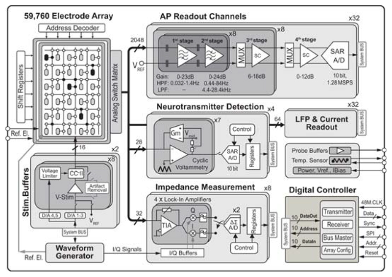
Since neuronal signal transmission is (electro-)chemical, and since local fluctuations of ion concentrations, as well as anisotropic and inhomogeneous electrical conductivity of tissue and culture medium are critically influencing electric interaction with neurons, we developed a multi-functional high-density MEA system while advancing characteristic features (Fig. 22.8.1). This monolithic system incorporates a large high-density electrode array of 4.48×2.43mm2 including 59,760 electrodes at a 13.5μm pitch (5487 electrodes/mm2) to record from large preparations/networks at subcellular resolution and the following circuitry units: 2048 action-potential (AP, bandwidth: 300Hz to 6kHz) readout channels, 32 local-field-potential (LFP, bandwidth: 1Hz to 300Hz) readout channels, 32 current recording units, 32 impedance units, 16 dual-mode voltage/current stimulation units, and 28 neurotransmitter measurement units.
Figure 22.8.1. Block diagram of multi-functional MEA system.
The system architecture critically relies on the SM approach [5], as we want to deliver every system function to any arbitrarily selectable electrode/electrode sets to perform, at the same time, stimulation and measurements of various cell or network parameters in parallel. Each electrode (Pt, 3×7.5μm2) is included in a 13.5×13.5μm2 pixel, along with 4 switches and 3 SRAM cells for switch control. Neuronal signal lines are all shielded with analog supply/ground tracks to minimize crosstalk. In addition to the higher electrode density, the largest high-density block here consists of 45x45 electrodes (Fig. 22.8.3), which is 4-times that in [5], due to technology scaling (0.18μm CMOS) and more metal layers. Array reconfiguration takes up to 4.5ms.
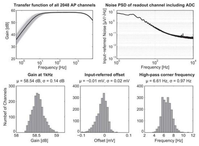
Figure 22.8.3. Measured Gain, offset and noise of AP readout channels.
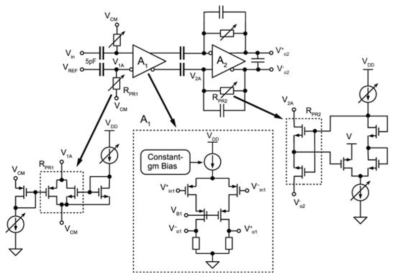
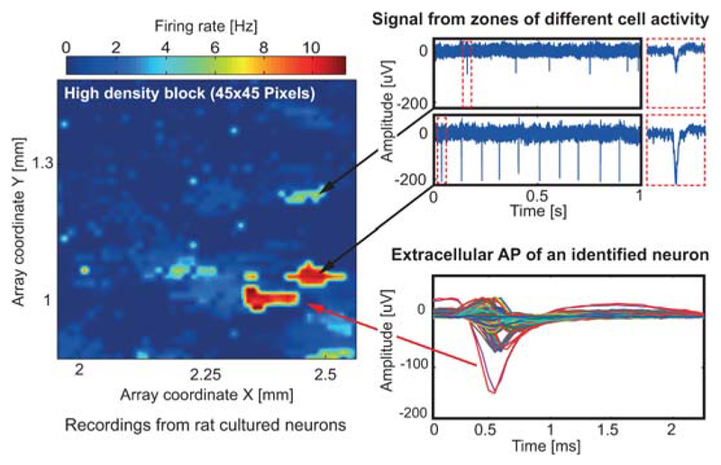
Both, AP and LFP signal readout was implemented and optimized for distinct characteristics of the two types of signals without increasing overall readout unit complexity. However, we here focus on the AP recording channels due to space limitations. Each AP channel consists of four fully-differential stages. The total gain can be programmed in steps of 3dB from 29dB to 77dB. A schematic of the first 2 stages is shown in Fig. 22.8.2. The 1st stage amplifier (A1) employs an openloop topology with resistive load to achieve low noise levels. Such topology avoids active loads that are usually implemented with NMOS transistors, which have higher 1/f noise levels than PMOS. Instead, resistors do not generate 1/f noise, and their thermal noise contribution is lower than that of active loads. A constant-gm biasing circuit has been used to generate the bias current of A1, which results in nearly uniform gain across all channels, as evidenced by measurements in Fig. 22.8.3. The 2nd stage features a closed-loop structure and anti-aliasing filtering. A first-order HPF is implemented in both stages. In the 1st stage, the HPF removes low-frequency drifts of electrode potentials. In the 2nd stage, HPF nulls the offset of A1. As the offset of the 2nd-stage amplifier is reduced by its closed-loop gain due to the DC feedback, the measured maximum input-referred offset of all AP channels is less than 0.11mV (Fig. 22.8.3). However, a huge resistance (TΩ) is required to build the two HPFs with very low corner frequencies (fHPF < 10Hz). So called “pseudo resistors” (MOS transistors biased in the weak inversion region) have been widely used, but their resistance may considerably vary across channels. Here, two new pseudo resistor structures have been devised (Fig. 22.8.2). Aided by the two current mirrors and level shifters, the first-order dependence of the overdrive voltages of the transistors inside RPR1 and RPR2 on their threshold voltages is cancelled out. Thus, RPR1 and RPR2 variations are substantially reduced, which leads to small fHPF variations (Fig. 22.8.3). Moreover, fHPF can be easily adjusted through the bias currents. The 3rd and 4th stages have been implemented with switched-capacitor amplifiers. An 8-to-1 multiplexer is realized in front of each stage so that all 64 neural signals can be sampled at 20KS/s and digitized by a 10b 1.28MS/s SAR ADC. The measured noise PSD of the whole AP channel is shown in Fig. 22.8.3. Dissociated cortical cells of embryonic-day-18 Wistar rats were cultured over 3-to-4 weeks on the chip. Recorded neuronal APs are shown in Fig. 22.8.4. Spontaneous activity, an area scan and single-electrode traces are displayed. All experiments were conducted inside an incubator at constant temperature (37°C) and 5% CO2.
Figure 22.8.2. Schematic of AP readout channel with pseudo resistors.
Figure 22.8.4. Activity map of cultured rat neurons.
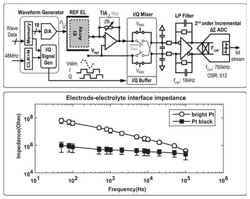
A schematic of the 32 lock-in amplifiers is displayed in Fig. 22.8.5. These units can measure the impedance of neuronal tissue in real time over a wide frequency range (1Hz to 1MHz). An on-chip generated sinusoidal voltage is applied between the internal reference electrode and all selected micro-electrodes. The impedance magnitude and phase response are then measured by a low-noise TIA and two quadrature phase mixers. A passive type mixer is used to mitigate 1/f noise and accommodate large signals. I/Q mixing signals are generated from the aforementioned waveform generator so as to get them phase-locked with the sinusoidal signal. The output DC signals from the mixers are low-pass filtered and digitized using two 2nd order discrete-time incremental ΔΣ converters. Impedance measurements of bright Pt and Pt-black electrodes in saline are shown in Fig. 22.8.5.
Figure 22.8.5. Impedance spectroscopy unit and measurement results.
Shown in Fig. 22.8.1, 16 stimulation buffers allow for simultaneous stimulation of multiple cells on different electrodes in current and voltage mode. Three DACs shared by each block (consisting of 8 buffers) are used to generate specified stimulation pulses. Two DACs, along with the voltage limiter, placed in the feedback path, are used to avoid reaching excessively high voltages in currentmode. By disconnecting the current conveyor (CCII) from the electrode upon reaching a pre-set value, accidental electrolysis and cell damage are avoided. Artifact removal is achieved by storing the electrode resting potential on a capacitor before stimulation and by re-applying that potential after stimulation.
Illustrated in Fig. 22.8.1, 28 cyclic-voltammetry circuits in blocks of 7 units are used to detect the release of neurotransmitters. To avoid changes in the overall cell solution potential and to enable simultaneous extracellular recordings, the working electrode potential is varied, while the reference electrode potential is kept constant. When scanning the working electrode potential, the designed TIA converts the electrode current to an output voltage. Meanwhile, the linear Gm cell blocks the feedforward path and obviates the coupling of the sweeping potential to the output. The output voltage is then multiplexed and digitized by a 10b SAR ADC.
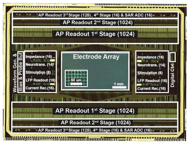
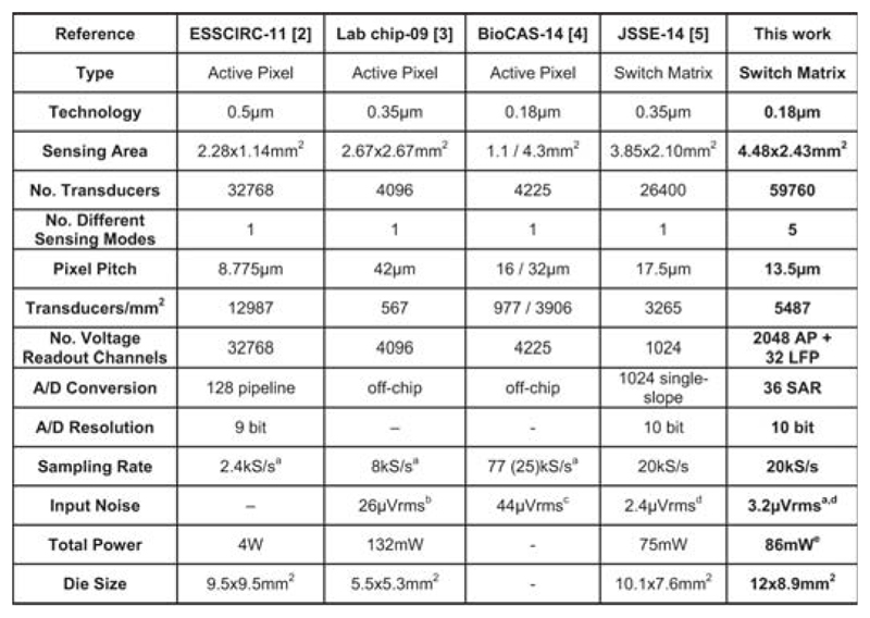
We demonstrate a multifunctional monolithic MEA system (Fig. 22.8.7) featuring the largest high-density (13.5μm pitch) electrode array to date, in which every electrode can be connected to various functional circuitry units. Its main specifications are compared with prior works in Fig. 22.8.6. Up to 2048 electrodes can be simultaneously used for recording at noise levels as low as 3.2μVRMS and meanwhile, stimulation, impedance measurements can be performed to detect cell positions/morphologies, or neurotransmitter release can be measured. This system is an enabling tool for in-depth neuroscientific studies targeting subcellular–resolution details or large complex networks.
Figure 22.8.7. Chip micrograph.
Figure 22.8.6. Comparison to previously published MEAs.
Acknowledgements
The authors thank M. Radivojevic, M. Ballini, P. Livi, D. Bakkum and U. Frey for help. Financial support through ERC Advanced Grant 267351 “NeuroCMOS” and individual support for A. Shadmani through FP7-MTN “EngCaBra” (Contract 264417) is acknowledged.
References
- [1].Obien M, et al. Revealing Neuronal Function through MEA Recordings. Front Neurosci. 2015 Jan;8:1–30.:423. doi: 10.3389/fnins.2014.00423. [DOI] [PMC free article] [PubMed] [Google Scholar]
- [2].Eversmann B, et al. A neural tissue interfacing chip for in-vitro applications with 32 k recording/stimulation channels on an active area of 2.6 mm. Proc ESSCIRC. 2011 Sep;:211–214. [Google Scholar]
- [3].Berdondini L, et al. Active Pixel Sensor Array for High Spatiotemporal Resolution Electrophysiological Recordings from Single Cell to Large Scale Neuronal Networks. Lab Chip. 2009 Sep;9:2644–2651. doi: 10.1039/b907394a. [DOI] [PubMed] [Google Scholar]
- [4].Bertotti G, et al. A CMOS-based Sensor Array for in-vitro Neural Tissue Interfacing with 4225 Recording Sites and 1024 Stimulation Sites. IEEE Trans BioCAS. 2014 Oct;:304–307. [Google Scholar]
- [5].Ballini M, et al. A 1024-Channel CMOS Microelectrode Array with 26,400 Electrodes for Recording and Stimulation of Electrogenic Cells In Vitro. IEEE J Solid-State Circuits. 2014 Nov;49:2705–2719. doi: 10.1109/JSSC.2014.2359219. [DOI] [PMC free article] [PubMed] [Google Scholar]


