Abstract
This paper presents a bio-inspired event-driven neuromorphic sensing system (NSS) capable of performing on-chip feature extraction and “send-on-delta” pulse-based transmission, targeting peripheral-nerve neural recording applications. The proposed NSS employs event-based sampling which, by leveraging the sparse nature of electroneurogram (ENG) signals, achieves a data compression ratio of >125×, while maintaining a low normalized RMS error of 4% after reconstruction. The proposed NSS consists of three sub-circuits. A clockless level-crossing (LC) ADC with background offset calibration has been employed to reduce the data rate, while maintaining a high signal to quantization noise ratio. A fully synthesized spiking neural network (SNN) extracts temporal features of compound action potential signals consumes only 13 μW. An event-driven pulse-based body channel communication (Pulse-BCC) with serialized address-event representation encoding (AER) schemes minimizes transmission energy and form factor. The prototype is fabricated in 40-nm CMOS occupying a 0.32-mm2 active area and consumes in total 28.2 μW and 50 μW power in feature extraction and full diagnosis mode, respectively. The presented NSS also extracts temporal features of compound action potential signals with 10-μs precision.
Index Terms: Peripheral nerves, Neural recording, Body channel communication, Neuromorphic, Level-Crossing ADCs, Neural sensors, Electroneurogram (ENG), Action potentials, Spiking Neural Networks, Feature extraction
I. Introduction
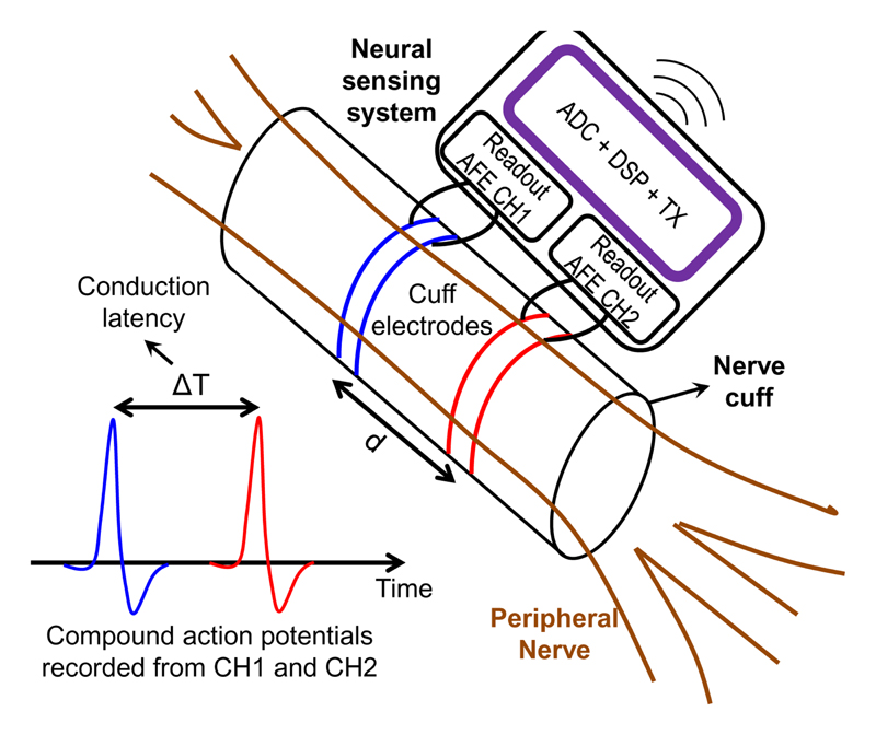
THE peripheral nervous system (PNS) can be seen as a “highway” for propagating neuron firings, i.e., action potentials (AP), for the bidirectional communication between the central nervous system (CNS) and various organs. The electroneurogram (ENG) can be measured with a nerve cuff or a neural probe surrounding or penetrating the peripheral nerves, respectively. Nerve ENG provides rich clinical information for diagnosis and can be the source of modulating human health as electroceuticals [1][2]. Decoding of the firing pattern of afferent compound action potentials (CAPs), the result of summation of many APs from the individual axons in a nerve trunk, holds the promise for indirect sensing of clinically relevant information, e.g., inflammation status or glucose levels, which can be employed in future electroceutical closed-loop applications [3]. Next, the CAP peak-to-trough duration and nerve conduction velocity (NCV) [4] are widely used diagnostic tools for various neuropathies. The requirement on temporal precision for such measurements is strict since the CAPs typically last for approximately one millisecond. This precision is especially challenging for NCV studies [5], which measures the time difference between peaks of two CAPs recorded from two locations on the same nerve, as shown in Fig. 1. To achieve high accuracy of NCV with a miniature nerve implant, temporal precision of the recording should be in the order of 10’s of μs, since NCV of a myelinated nerve can be up to 120 meter/s. Better temporal precision of the recording allows the volume of the nerve implant (e.g., nerve cuff) to be further miniaturized. To achieve such temporal precision, the analog-to-digital converters (ADCs) in a conventional neural recording system need to have a sampling rate of 10’s of kSample/s (kSps), which is 10-100× higher compared to the sampling of other electrocardiogram (ECG) signals. This increases the energy consumption not only in wireless transmission, but also in local processing, storage, and transportation of the data.
Fig. 1. Concept illustration of neural recording of peripheral nerves, and the conceptual illustration of nerve conduction velocity measurement.
In order to have high spatial selectivity, neural implants for peripheral nerves should be placed very close to the surface (or inside) of the nerve, as illustrated in Fig. 1. To avoid nerve tissue damages, such nerve implants should have strict volume and energy constraints. A nerve implant with a volume in the millimeter-scale is highly preferred. Since there is no sufficient volume for a battery, the electronic system should consume low energy well below 100 μW, to enable wireless power transfer.
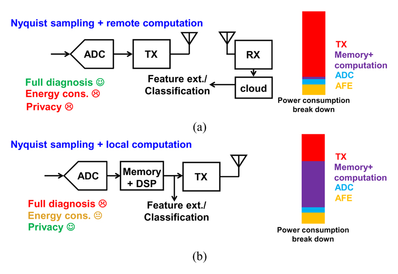
Fig. 2 shows two conventional architectures of implantable sensing systems, which typically consist of one or multiple channels of analog front-end (AFE), ADC, digital signal processing (DSP), memory, and a wireless transmitter (TX). These architectures are based on Nyquist sampling, but one replies on remote computation (Fig. 2(a)) and another one has embedded local computation (Fig. 2(b)). The first architecture is suitable for diagnosis purposes. The high-precision raw sensor data sampled by the Nyquist ADCs are sent wirelessly to a remote hub to perform further data processing. However, such “frame-based” sampling produces a large amount of data from neural recording, which will consume high wireless transmission energy [6][7]. In addition, performing the computation remotely may introduce potential privacy concerns.
Fig. 2. Conventional architectures of sensing system.
(a) Nyquist sampling with remote computation; (b) Nyquist sampling with local computation.
Fig. 2(b) shows an alternative approach based on near-sensor local computation, e.g., feature extraction or classification, to reduce the burden on data transmission. However, this approach requires power- and volume-hungry computation and storage hardware, which is not affordable with a millimeter-scale nerve implant. In addition, such architecture may not be suitable in practice, if raw data are not available in case personalization or detailed diagnosis is needed. Reference [7] uses a local processor to extract ECG signal features, but it requires a relatively large memory (46 kByte) and high-power consumption (~60 μW) for detecting only the peak of the ECG signal, i.e., the R wave. Nevertheless, full ECG features (P, QRS and T waves) are still crucial for accurately detecting many cardiac abnormalities, e.g., arrhythmias.
ENG signals have very sparse activity (typically <10 CAPs per second), but a high temporal resolution is still required. High redundancy will be generated, if these signals are sampled with conventional high sampling rate Nyquist ADCs, thus leading to a poor system efficiency. Inspired from biology [8] [9], the energy consumption of information processing and transportation can be significantly reduced if only the changes (i.e., delta) of the signal are processed, while information can still be recovered on the reception side with high resolution. One example of such a sensing system is our retina, whose neurons only fire when detecting temporal changes from photoreceptors. The action potentials fired from retina neurons are transmitted through an optic nerve with quite limited data capacity and energy budget, but our brain (the receiver of information) has no problem reconstructing high-quality images. This concept is also suitable for implantable neural sensing systems with very limited energy sources.
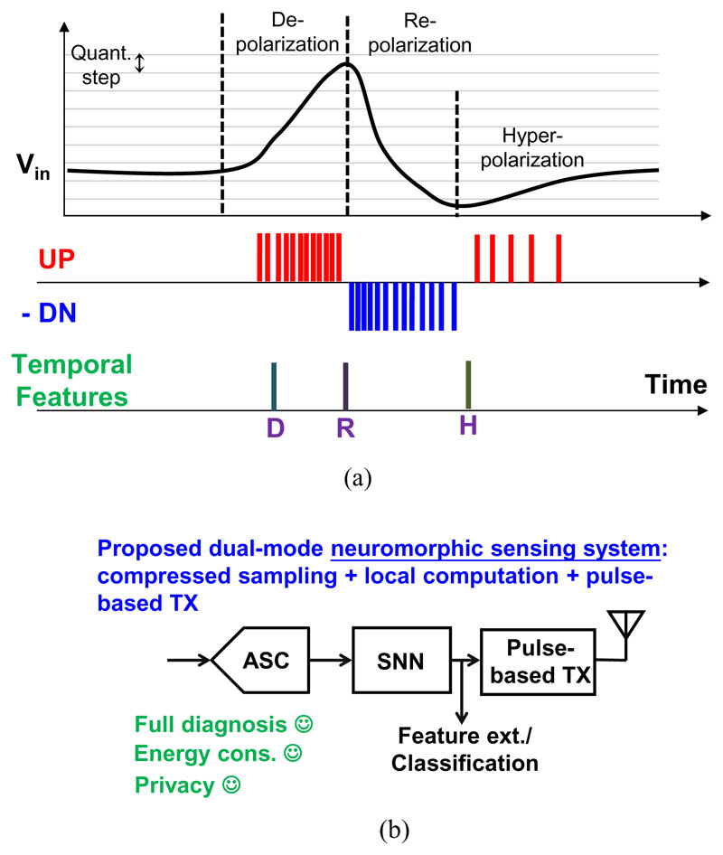
Fig. 3(a) illustrates one example waveform of a CAP. Instead of processing signals with a constant clock in every frame, the system is active only if there are CAPs. This significantly reduces the data rate, and thus the requirements of the hardware as well as the energy consumption. Furthermore, the temporal feature can be well preserved, without being limited by the sampling grid of Nyquist ADCs. To implement such bio-inspired sampling mentioned above, an analog to spike converter (ASC) based on level-crossing ADCs (LC ADC) can be employed to perform “delta encoding” [10], which reports (up or down) events when changes larger than a certain threshold are detected. As shown in Fig. 3(a), the ASC generates UP or DN pulses when the CAP signal crosses one quantization (or threshold) step with a positive or negative slope. This greatly reduces the temporal redundancy.
Fig. 3.
(a) Delta encoding of ENG CAPs, and its temporal features D, R, and H; (b) The conceptual block diagram of the proposed Neuromorphic Sensing Systems.
Different implementations of such delta modulation have also been presented in other low-power neural recording systems. In [11], a Δ-ΔΣ analog front-end architecture is proposed, but a higher over-sampling ratio (for noise-shaping) significantly increases the data rate. In [12], an analog-based delta modulator is implemented prior to a Nyquist SAR-ADC but requires a large capacitor area for implementing analog differentiators and a programmable threshold for optimum spike detection. Furthermore, both approaches in [11] and [12] require a precise external clock based on an off-chip crystal, increasing both form factor and power consumption.
Fig. 3(b) shows this proposed neuromorphic sensing system (NSS) concept [13]. It includes an ASC for delta encoding, a spiking neural network (SNN) for local computation, and a pulse-based transmitter tailored for low-energy event-driven transmission. The event-based nature of the NSS not only improves the energy efficiency by exploiting the sparse nature of CAP signals, but also avoids a power-hungry system clock generation and synchronization circuits. Most importantly, the temporal precision is no longer limited by the fixed sampling grid of the clock.
The proposed NSS is designed to support dual-mode operation: full diagnosis and feature extraction mode. The capability of dual-mode operation is crucial for implantable sensing devices since detailed diagnosis is required in case of urgent situations, e.g., implant failure. When the NSS is in the feature extraction mode, only the extracted temporal features (i.e., labels) are transmitted out for energy saving, or they can be decoded and fedback to the implant stimulator to perform closed-loop neuromodulations. Fig. 3(a) shows that three temporal features can be extracted from CAPs, i.e., depolarization (D), repolarization (R) and hyperpolarization (H). They can be detected from the polarity and density of the spike trains [14]. When a full diagnosis is required, the NSS programs the ASC to have higher precision and the pulse-based TX to operate at a higher event transmission rate, so that raw CAP signals can be transmitted in full detail.
The rest of this article is organized as follows. Section II discusses the proposed architecture of NSS and its design trade-off. Section III describes the implementation of the circuits. The measurement results will be shown in Section IV. Finally, Section V presents the conclusions.
II. Proposed Architecture and Design Trade-Offs
This section discusses in detail the proposed NSS architecture. The design trade-off between quantization error and event transmission rate will also be provided.
A. Architecture Overview
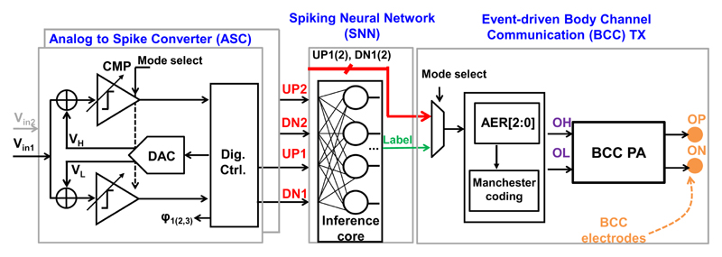
Fig. 4 shows more detail of the presented NSS, including two ASCs, an SNN and a pulse-based body channel communication (BCC) PA. This work focuses on the sampling, processing and transmission of the event-driven neural sensing, and the AFE front-end (i.e., low-noise amplifier and band-pass filter) of the neural interface is not included. This work demonstrates two channels, which is the minimum channel number required for performing a conductive velocity study. The number of sensing channels can be easily scaled in the proposed NSS, based on the requirements and constraints of different clinical use cases. Two ASCs are implemented as level-crossing ADCs (LC-ADCs). LC-ADCs perform delta encoding, so they also have better immunity to low-frequency noise and are able to reject the input DC offset, compared to other ADCs.
Fig. 4. The detailed block diagram of the presented NSS, including ASC, SNN and BCC PA.
Conventional neural network (NN) architectures either cannot support event-driven operation [15], or use analog-intensive neurons and synapses which are sensitive to PVT variations [16], and both still consume relatively high power (100’s of μW). Asynchronous event-driven processing allows the NN to be active only if events occur. Therefore, a low-power and fully synthesizable SNN has been chosen as the local data processor in this work (details to be discussed in Section III-B). Inspired by natural computing in the brain, neuroscientists modeled synaptic interactions between neurons, considering the time of spike firing [17]. Compared to a conventional neural network, the input of SNNs is in the rate of events instead of a digitized amplitude and the output of SNNs is also represented by asynchronous events. Four outputs of two ASCs (UP1, DN1, UP2, and DN2) are connected to the SNN which is only active when there are CAPs. Thanks to the reduced temporal redundancy, the memory needed for the SNN to extract the signal features and generate corresponding labels is reduced by 2-10×. Note that this memory is distributed in SNN neurons, which also reduces the energy required for memory access.
Since the SNN mimics biological neural network and processes information in an asynchronous spike format, it can directly use the outputs from LC-ADCs, i.e., up or down spikes. If conventional clocked ADCs are adopted, an extra digital translation circuit and an clock generation are required, which increases hardware complexity, power consumption and potentially degrades the temporal resolution.
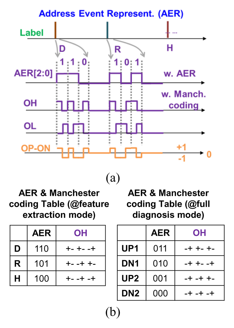
In feature extraction mode, the SNN inference core can generate three temporal labels (D-R-H), which are then encoded with a serialized form of address-event representation (AER) [18]. In full diagnosis mode, four outputs from two ASCs are directly encoded. The AER output is further encoded with Manchester code before the BCC transmission, minimizing the residue charge in the tissue (to be detailed in Section III-C).
B. System Analysis and Design Trade-offs
To achieve the targeted temporal and amplitude resolution in neural recording, conventional Nyquist ADCs are typically designed with a high dynamic range up to 10-bit resolution and sampled with high frequency up to 30 kSps [19]. A large amount of data needs to be transferred to an external device wirelessly, resulting in a high data rate of up to 300 kbps each channel in full diagnosis mode. As reported in [20], the data transmission consumes more than 90% of the total system energy. The proposed NSS reduces the data rate by leveraging the sparse nature of CAP signals.
For a Nyquist sampling system, the ADC’s clock defines the time stamps and thus the precise timing of the rest of the system (including wireless link) is not critical because the time stamps are already defined together with the data. However, in this clock-less event-based sampling system, the time stamps are set based on the timing of the received wireless data, i.e., time itself represents the time stamps, and thus timing variation in the entire chain affects temporal precision. The system timing resolution also determines the signal quality after reconstruction. The timing resolution can be limited by many parts of the NSS. One dominant limitation is the maximum event transmission rate the NSS can achieve, or equivalently how fast two events can be transmitted consecutively. If one event packet, i.e., an event with serial address-event representation, has a long length in time, the transmission of the following event must be delayed, which equivalently introduces a time-domain quantization error.
To minimize the length of event packets (or maximize the event transmission rate), the bit period must be reduced. However, this requires a higher speed of the Pulse-BCC PA, which also consumes more power. To understand the relation between the maximum required event transmission rate and the signal quality after reconstruction, analysis based on a numerical simulation are performed and validated. In this analysis, a synthetic action is converted to UP/DOWN events by the ASC. Note the event rate is coupled to the number of bits (or the quantization steps) of the ASC, i.e., finer quantization steps produce more events.
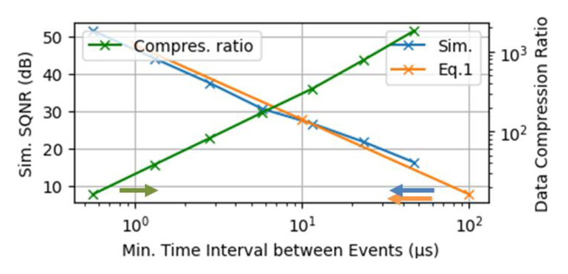
Since the SNR of recorded APs in-vivo is typically limited to 20 dB [21] due to biological noise and wide signal bandwidth, the target of the maximum signal-to-quantization-noise-ratio SQNR is set to 25 dB in this work. Based on the analysis provided in [22],
| (1) |
where δ is the timing uncertainty of the event-based system; fSIG is the signal bandwidth, which is ~1 kHz for the nerve’s CAP signal. To achieve an SQNR of 25 dB, the system timing uncertainty should be less than 10 μs. To meet this timing uncertainty requirement, the speed of the LC ADC, the latency of the SNN and the length of the event packet need to be optimized (to be detailed in Section III) to ensure the NSS does not miss events when the input signal slope is large.
Fig. 5 shows the relation between the required timing resolution and the simulated SQNR, which matches well with the theoretical results from Eq. (1). Fig. 5 also shows a simulated data rate reduction compared to conventional Nyquist sampling and frame-based transmission. The firing rate of CAP is 10 Hz, and the AER overhead has been included for the event transmission. It shows that the proposed NSS can achieve higher than 200× of data reduction, while keeping SQNR above 25 dB.
Fig. 5. Simulated SQNR versus minimum time interval between two events and the simulated data rate compression ratio.
III. Circuit Implementation
Three circuit innovations will be discussed in this section: (1) a background offset mitigation technique is proposed to enhance the offset tolerance of ASCs; (2) a fully synthesized low-power SNN is introduced, which is capable of on-chip temporal feature extraction; (3) a power amplifier (PA) with charge balancing and AER encoder for event-driven Pulse-based Body Channel Communication (Pulse-BCC) is introduced.
A. LC ADC with the Offset Calibration
Several area- and energy-efficient LC ADCs have been presented in [23–25]. An adaptive sampling scheme has been presented in [23] and achieves low power consumption (61 nW in [23]). However, its SNDR (35 dB) is limited due to the comparator offset. Ref. [24] implements an offset calibration and improves its SNDR, but also at the same time increases chip area. In [25], a two-tier approach has been proposed to achieve high SNDR (up to 57 dB) by applying more than ten comparators to track the analog signal with fine steps, at the expense of high power and large chip area. To mitigate the comparator offset without significantly increasing area, a new background comparator offset calibration is explored in this work.
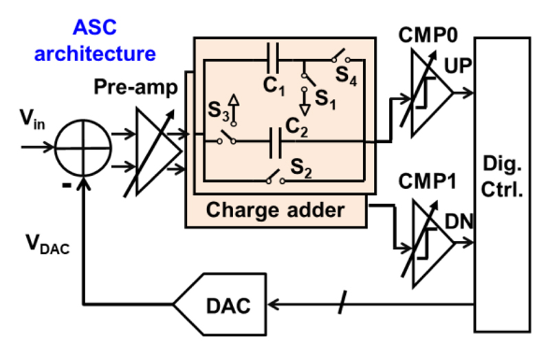
The block diagram of the LC ADC is shown in Fig. 6. The ADC continuously monitors the input signal and generates an UP or DN event when the input change crosses a +1 LSB or -1 LSB threshold, respectively. To do so, the analog input signal is diminished by a voltage generated by a digital-to-analog converter (DAC), VDAC. After the subtraction, a pre-amplifier amplifies the signal and two charge adders add and deduct 1 LSB from the signal, respectively. Two continuous-time comparators are employed to detect when the zero-crossings occur. If it happens, a digital control block (Dig. Ctrl.) will update VDAC and wait for the next zero-crossing.
Fig. 6. Architecture of the LC ADC.
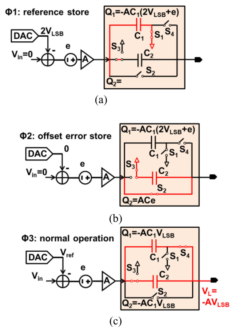
The LC-ADC employs two comparators to actively detect rising and falling zero-crossings. However, the offset difference between these two comparators, degrades SNDR of the LC ADC. Therefore, a background offset mitigation technique is proposed and shown in Fig. 7. Instead of using two separate comparators, the first stage (pre-amp) is shared between them so that the offset errors of the second stage are divided by the pre-amp gain A. Then, a double-sampling switched-capacitor circuit removes the offset error e of the pre-amp and stores the two threshold levels (VH and VL) in three steps.
Fig. 7. Background ASC offset cancellation at different phases.
(a) reference store; (b) offset error store; (c) normal operation.
First, the reference levels ±VLSB and the offset e are amplified by A and stored on capacitor C1. Second, only the amplified offset error e is stored on another capacitor C2 whose capacitance is the same as C1. Third, as the normal operation, C1 and C2 are connected, the offset error e is cancelled, and the input-referred voltage is shifted by means of the capacitors is ±VLSB for the threshold voltages VH and VL. These operations are controlled by three non-overlapping signals φ1-3, which only toggle in the presence of UP or DN pulses. To support dual-mode operation, the pre-amp and the comparators can be programmed with different power and bandwidth.
From the discussion in Section II.B, the maximum timing uncertainty (i.e., delay) should be less than 10 μs, which sets the maximum delay of the ASC. The delay of the ASC is determined by the bandwidth of the pre-amplifier and the comparator, the delay of the digital control and the settling time of the DAC and the charge adder. Among them, according to the simulations, the settling time of the charge adder is the dominant delay.
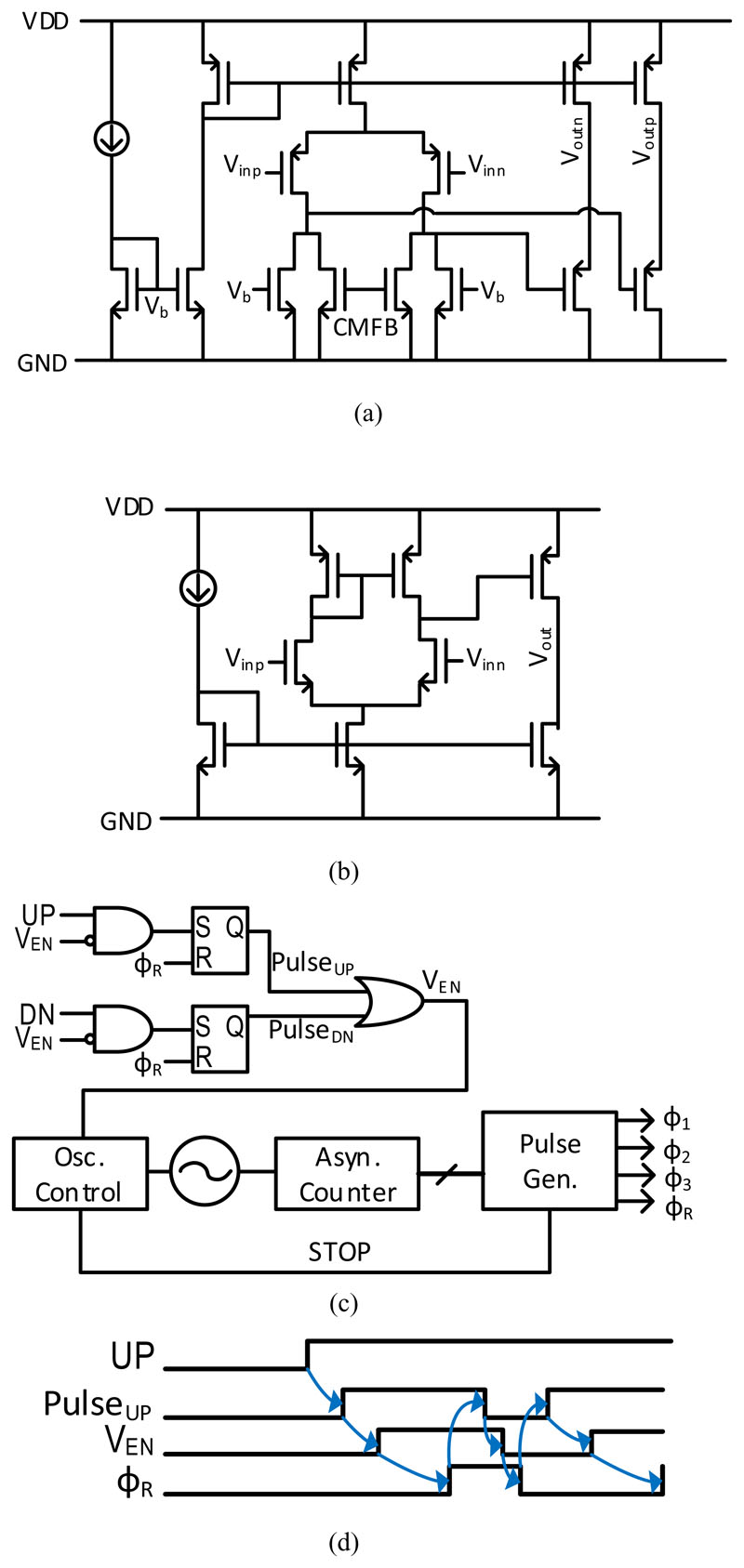
Fig. 8(a) shows the implementation of the pre-amplifier which is a differential pair with an NMOS load, and the input range is from 0 to 1 V. This amplifier is designed to have a gain of 10 dB, which is large enough to relax the offset requirement of the comparator but is still linear enough with an input amplitude range of ±1 LSB. The input-referred noise is designed to be 223 μVRMS and the bandwidth is 9.5 MHz, in order to achieve the target SNR requirement. The implementation of the comparator is shown in Fig. 8(b) and this comparator achieves a gain of 85 dB, a bandwidth of 6.7 MHz, and an input-referred noise less than 30 μVRMS. A 6-bit DAC is implemented with a unit capacitance of 1.6 fF to meet the matching requirement. The capacitance of C1 and C2 in the charge adder is chosen to be 50 fF to have sufficient charge hold time. With this capacitance value, the settling time of the charge adder is less than 1 μs, which is approximately one order shorter than the timing uncertainty requirement.
Fig. 8.
(a) Schematic of pre-amplifier; (b) schematic of comparator; (c) schematic of control signal generator with anti-self-locking scheme; (d) timing diagrams of anti-self-locking scheme.
The implementation of the control signal generator is shown in Fig. 8(c). A ring oscillator starts oscillating when there is a flag of either an PulseUP or PulseDN pulse. An asynchronous counter counts the number of edges of the oscillator, which is then used to generate four non-overlapping pulses (φ1-3 and φR). Afterwards, the oscillator is disabled again to reduce power consumption.
LC-ADCs may not be able to track the analog input if self-locking [26] happens, which requires an anti-self-locking mechanism to increase the robustness of LC-ADCs, as shown in Fig. 8(c). The timing diagrams of the relevant signals are shown in Fig. 8(d). For instance, in case self-locking happens, the comparator output UP will remain high. The reset phase, φR, will be generated and then the signal PulseUP will be set to low. Hence, PulseUP pulses will occur until the comparator output returns to zero.
B. Fully Synthesized Low-power SNN
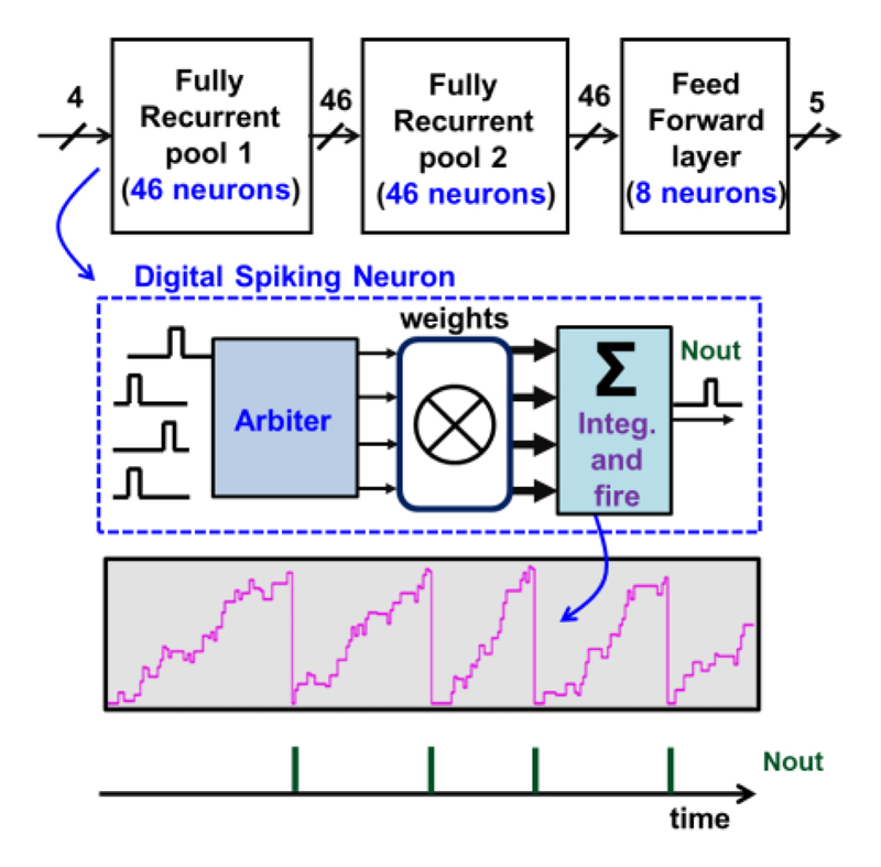
An SNN includes a massively parallel implementation of digital asynchronous spiking neurons whose membrane potential integrates inputs (i.e, spikes) from neighboring neurons. Once the membrane potential reaches the threshold, the neuron fires and generates a spike. The spatiotemporal spike patterns are used in an SNN to perform communication and computation. A low power fully synthesized SNN has been introduced in [27]. In this work, the SNN has been further adapted for the implantable neural sensing application. Using a synthetic dataset of neural signals in the simulation, we have explored parameters for the most suited network size, the number of bits for the synaptic resolution, membrane potential accumulator size, and the number of neurons per layer as well as the number of layers.
The implementation of the SNN is shown in Fig. 9. To exploit the sparse activity of the ENG signals, the network is made self-timed, resulting in near-zero dynamic power dissipation in the absence of any input activity. By a trade-off between the complexity of the neural network and the cost of the hardware, the SNN consists of two consecutive pools of fully recurrently connected spiking neurons and each pool contains 46 neurons.
Fig. 9. Block diagram of the fully synthesizable SNN core.
These pools are followed by a fully-connected layer with 8 neurons. A stream of spikes (digital pulses) represents the network inputs and outputs, whereas the synaptic weights are stored with 8-b digital numbers. Note that digital spiking neurons provide more flexibility, lower power consumption and low sensitivity to PVT variations, compared to charge-based analog spiking neurons in [16].
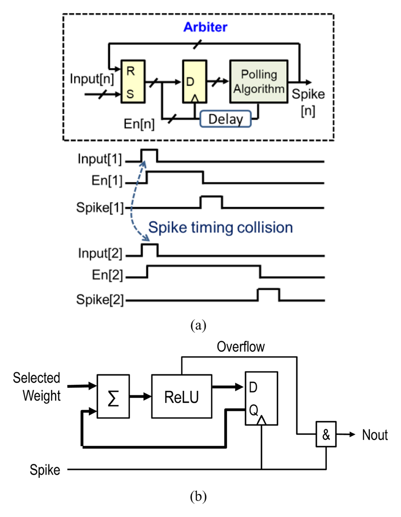
Additionally, Fig. 9 shows that a digital spiking neuron consisting of three parts: an arbiter, a weight selector and an integration-and-fire module. Input spikes arriving at arbitrary times select a corresponding weight, which gets added to an accumulator. When the digital accumulator overflows, it produces an output spike similar to biological neurons’ integrate-and-fire operation. To solve timing collisions, each neuron has an arbiter that adds a small time offset (100’s of ns) to set the priority using a “Round-Robin” polling algorithm. The simplified block diagram of the proposed arbiter and its waveform are shown in Fig. 10(a). The arbiter is implemented before each layer of neurons. It detects the presence of input spikes and dispatches them to the recipient neurons. Based on the spike input address, the weight selector sends the corresponding weight to the integration-and-fire module. Fig. 10(b) shows the implementation of the integration-and-fire module. An accumulator sums the selected weights, and a Rectified Linear Unit (ReLU) is implemented after the accumulator to ensure that outputs are always positive. When the accumulator overflows (i.e., a neuron passes the threshold), an output spike is generated and sent to the arbiter of the next layer. This SNN is fully synthesized by the standard digital design flow. More details on the circuit implementation can be found in [27].
Fig. 10.
(a) Simplified block diagram of arbiter and its waveform; (b) simplified block diagram of integration and fire module.
Since the temporal pattern of the CAP signals is important, the SNN needs to have a fast response time when extracting features. The spike arbiters determine the speed of the SNN. Every neuron layer contains such an arbiter. The largest one is at the second layer and has N=46 spike inputs. The delay Tcycle of the arbiter to process one spike is mainly determined by its embedded priority encoder. With Tgate being a typical logic gate delay in this technology, we found:
| (2) |
Then, the number of spikes per second that can be processed by the arbiter is 1/Tcycle. For example, in 40nm CMOS, Tgate=40 ps. If N=46, then Tcycle = 3*8*40 ps =1 ns. This delay has a negligible impact on temporal uncertainty.
An offline supervised training strategy presented in our prior work [28] can be adopted for the presented SNN, which exploits a surrogate gradient approach and Backpropagation-Through-Time (BPTT). Due to the lack of labeled ENG datasets, and the training of the SNN is also beyond the scope of this work, the weights of the presented SNN are chosen based on the simulation, to demonstrate its capability of temporal feature extraction.
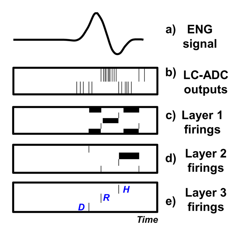
Fig. 11 shows the simulated SNN activities. The hardware model of integrate-and-fire neurons is adopted, taking into consideration its fixed-point operations. The events coming from the LC-ADC are shown in Fig. 11(b). The two layers of neuron pools implemented in the SNN are visible in Fig. 11(c) and Fig. 11(d), where black lines represent internal neuron firings. In Fig. 11(e), the last layer of the network shows the activity of output neurons responsible for extracting temporal features of the ENG signal (D, R, H).
Fig. 11.
SNN simulated activity. Input patterns are ENG signals from the measurement, and the classification task is labeling the different parts of the ENG, as in [13] and [28].
C. Pulse-BCC PA and Address-Event Representation (AER)
Instead of adopting high-frequency EM radiation [7][29][30], galvanic-coupled body-channel communication (BCC) is adopted in this work for the following reasons. First, it does not require an antenna, so the NSS volume can be miniaturized. Second, it has lower propagation loss inside the human body. And third, it also provides better privacy since the signals do not radiate [31].
The body channel is modeled with a finite element method using COMSOL Multiphysics, based on the dielectric properties provided in literature [32]. Based on this channel model, the PA design specifications are determined, including driving strength, settling time, charge balance, etc. The baseband data is encoded with Manchester encoding scheme, and the bit period can be programmed from 0.5 to 2 μs, which corresponds to a frequency band of 100’s of kHz to a few MHz. As the body channel has a bandpass characteristic, the high pass corner frequency is determined by the value of the AC-coupling capacitance and the double-layer capacitance of the electrode-tissue interface. The simulated high-pass corner frequency in this work is below 1 MHz, and the simulated path loss approximately 35 dB.
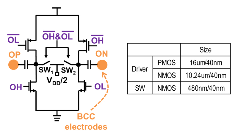
The differential PA, as shown in Fig. 12, generates a positive output when OH is high and a negative signal when OL is high. The PMOS and NMOS need to be properly sized to have similar on resistance to minimize current imbalance, such that the charge accumulation on the tissue-electrode interface can be minimized. And the sizing of the transistors is shown in Fig. 12. When both OH and OL are low, the PA outputs are reset to half VDD, and it only dissipates 1.2μW. The on resistance of the reset switches, SW1 and SW2, needs to be small enough as it impacts the required reset time.
Fig. 12. Schematic of BCC differential PA.
In feature extraction mode, three temporal labels generated by the SNN will be coded with a serialized 3-bit AER, as illustrated in Fig. 13. The corresponding “address” of each label will be attached to the polarity of the event (either up or down), using a serialized 2-bit Tenary code (with “+”, “-”, and “0”). The AER output is further coded with Manchester coding, to ensure the number of “+” and “-” are always equal, which is important to ensure the charge balance. To transmit these AER coded labels, the differential Pulse-BCC PA either charges or discharges the tissue if the AER output is “+” or “-”. When the AER output is “0”, the reset circuit of the PA will short two ends of the BCC coupler and connect to half VDD, to further remove any residue charge in the tissue.
Fig. 13.
(a) Output waveforms from AER and BCC-TX; (b) AER and Manchester coding tables from two operation modes
According to the discussion in Section II-B, the event packet length should be less than 10 μs to ensure that the timing resolution of the event-based transmission is fine enough not to degrade signal quality. The event packet length can be calculated by
| (3) |
where n represents the number of bits for the AER and Manchester code (in this case is 6), Tbit is the period of each bit, and Treset is the time required for the reset circuit to remove the residue charge in the tissue. Note that Treset heavily depends on the strength of the reset circuit and the BCC coupler geometry, and it is ~4 μs in this work. The Pulse-BCC PA has a programmable bit period in the range of 0.5-2 μs.
IV. Measurement Results
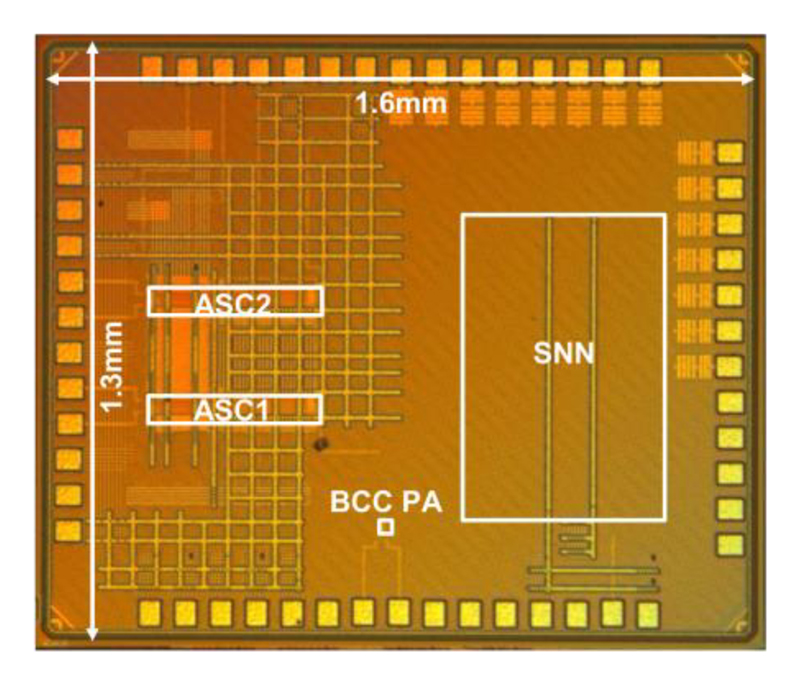
As shown in Fig. 14, the proposed NSS is fabricated in 40-nm CMOS technology and its active area is only 0.32 mm2, thanks to a reduced memory demand and the area-efficient Pulse-BCC.
Fig. 14. Chip photo in 40nm CMOS.
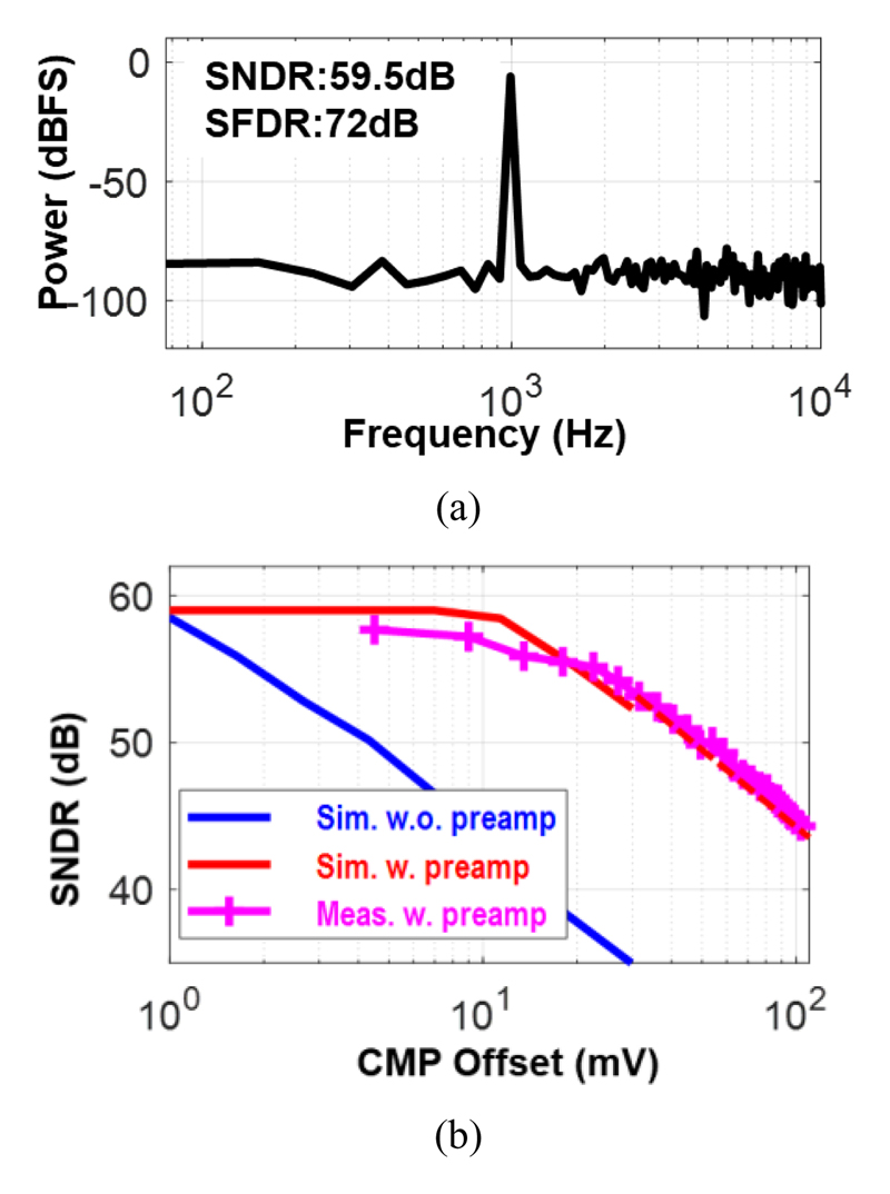
To evaluate the performance of the LC-ADC, a sinusoidal wave is set as the input. In feature extraction mode, the LC-ADC is configured in low power-consumption mode and it achieves 30-dB SNDR with 7-μW. In full diagnosis mode, at a higher power of 17-μW, it achieves 72-dB SFDR and 59.5-dB SNDR which is shown in Fig. 15(a). Fig. 15(b) shows the simulated and measured SNDR with different induced comparator offsets and the improvement could be observed after employing a pre-amplifier.
Fig. 15.
(a) Measured SNDR from ASC outputs. (b) Simulated and measured SNDR with different ASC comparator offset.
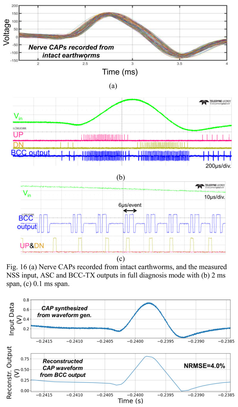
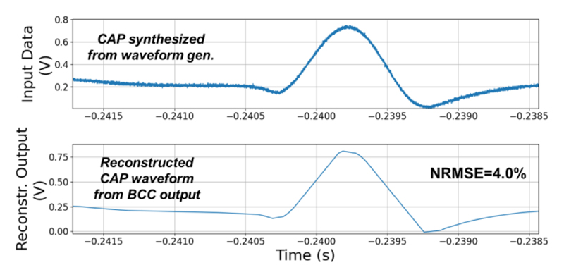
The NSS is characterized with a synthetic CAP waveform according to our neural recordings from intact earthworm’s medial giant nerve fiber, as shown in Fig. 16(a), which is widely used approach for studying neurophysiology [33]. It is provided as the input signal generated by a waveform generator, with an amplitude matched to the ASC’s full scale and a frequency of ~10 Hz (i.e., 10 CAPs per second). Fig. 16(b) and 16(c) show the outputs of the ASC and the Pulse-BCC TX outputs in full diagnosis mode. Fig. 16(c) shows the time domain waveform from the Pulse-BCC output with Manchester coded AER. The event packet length is measured to be ~6 μs. The reconstructed waveform from the Pulse-BCC TX output is shown in Fig. 17, where the reconstruction is implemented with a simple accumulation without any filtering. The measured Normalized RMS error (NRMSE) between the input and reconstructed signals is 4%, and the SQNR is estimated to be 27.9 dB, which is close to the analysis in Section II-B.
Fig. 16.
(a) Nerve CAPs recorded from intact earthworms, and the measured NSS input, ASC and BCC-TX outputs in full diagnosis mode with (b) 2 ms span, (c) 0.1 ms span.
Fig. 17. Measured normalized RMS error between the reconstructed CAP waveform based on the TX output, and the ASC input signal.
The measured power consumption of the SNN during the feature extraction is 2 μW and 11 μW for dynamic and leakage power, respectively. The SNN is only active when the input signals change substantially, leading to very low dynamic power. The leakage power is limited by the nanoscale transistors in the implemented process and can be further improved with advanced techniques or process [34].
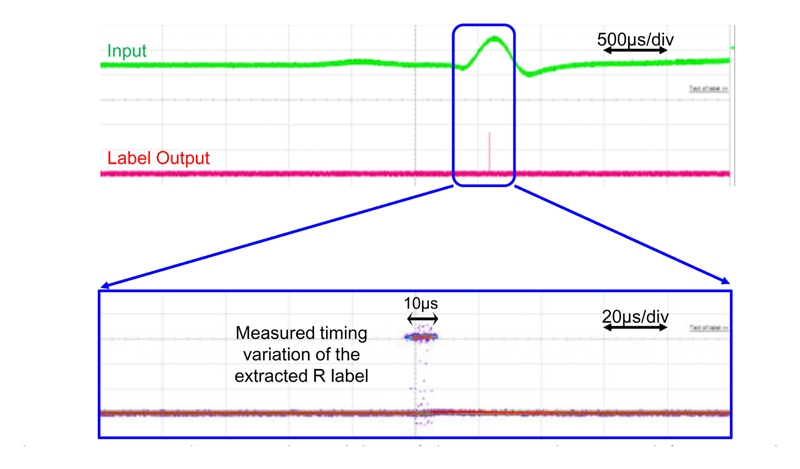
The temporal resolution is typically limited by the sampling period (e.g., ~33 μs in [6][35]) in conventional frame-based sampling systems [36]. The temporal resolution in feature extraction mode is measured by overlaying multiple of extracted R labels of the CAP and measuring the timing uncertainty, as shown in Fig. 18. The SNN is pre-trained to recognize the R feature of the synthetic CAP. The measurement result shows that a temporal precision of 10 μs can be achieved with the proposed event-based NSS.
Fig. 18. Measured temporal precision of the extracted temporal feature R, i.e., peak of the CAP, by overlaying multiple measurements.
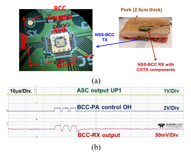
Fig. 19(a) shows the setup for the evaluation of the Pulse-BCC link. The electronic module area of the NSS, including the coupler of the BCC TX, is only 72 mm2. A PCB for the BCC receiver (RX) has been developed using commercially available components. A porcine tissue with 2.5-cm thickness has been used as the communication channel for the BCC link. Fig. 19(b) shows the TX input data and the received output from the RX.
Fig. 19.
(a) Measurement setup and the photo of the NSS module. The Pulse-BCC measurement is performed with a 2.5-cm porcine tissue. (b) Measured Pulse-BCC TX input and RX output signals.
The NSS consumes only 28.2 μW and 50.5 μW system power in the feature extraction and full diagnosis mode, respectively. Currently the system power consumption is limited by the leakage performance of the selected process. The comparison with state-of-the-art electrophysiology (ECG, ENG) sensing and data transmission systems is shown in Table I. Thanks to the bio-inspired event-based sampling, the data rate can be reduced by 125×, while achieving 10 μs temporal resolution. Note this compression ratio is with respect to a 30 kSps 10-b Nyquist ADC, and a CAP firing rate of 10 Hz. Although adaptive sampling techniques can also achieve a compression ratio of 7× [7], it requires complicated and power-hungry digital processing for mode control. Although finer temporal resolution can be achieved with a higher sampling frequency as in [28], this also leads to a higher system power consumption.
Table I. Comparison with state-of-the-art implantable sensing system.
| This work | [7] Kim TBIOCAS’14 | [24] Shon Sensors’17 | [25] Azin JSSC’11 | [37] Tochou JSSC’22 | [38] Jeon VLSI’19E | |||
|---|---|---|---|---|---|---|---|---|
| Tech. (nm) | 40 | 180 | N.A. | 350 | 28 FDSOI | 180 | ||
| Supply (V) | 0.9/1.1/1 | 1.2 | N.A. | 1.5 | 0.5 | 1 | ||
| System | ADC+SNN+TX | AFE+ADC+ DSP+TX | AFE+ADC +TX | AFE+ADC+ DSP+TX | TX | TRX | ||
| Applications | Implantable ENG (PNS) | Wearable ECG | Implantable ENG (PNS) | Implantable ENG (Brain) | Wearable | Implantable | ||
| Feat. Extr. | Full diag. | Feat. Extr. | Full diag. | |||||
| ADC architecture | LC (event-based) | SAR (Nyquist) | NA (Nyquist) | SAR(Nyquist) | N.A. | N.A. | ||
| Data rate/ch= ADC sample rate nr. of bits (bps) | <100 event/s | ~2.4k event/s | 512/64 (Adaptive) × 12b =877 | 10k×10b=100k | 35.7k × 10b =357k | N.A. | N.A. | |
| Data compression | >125×A | 7 × | 1 | 1 | N.A. | N.A. | ||
| Temporal precision (μs) | 10 | >2000B | - | >28B | N.A. | N.A. | ||
| ADC ENOB | 5 | 9.5 | 10.3 | N.A. | 9.1 | N.A. | N.A. | |
| TX freq./mod. | 0.5-μs Pulse based galvanic BCC | 2.4GHz BLE | 400MHz FSK | 433MHz FSK | 350-550MHz OOK capacitive BCC | 100Mbps galvanic BCC | ||
| Nr. of chan. | 2 | 3 | 2 | 8 | - | - | ||
| TotalC | 28.2 | 50.6 | 1060 | 13340 | N.A. | 274 | 17/76D | N.A. |
| Total power cons./Ch (μW)C | 14.1 | 25.3 | 330 | 4430 | N.A. | 34 | 17/76D | 475 |
| Active area (mm2)C | 0.32 | 8.46 | N.A | 2.43 | 0.0418 | 0.6 | ||
| System module area (mm2) | 72 | ~500 | 924 | N.A. | N.A. | N.A. | ||
| On-chip labeling | D/R/H | - | Peak (R) only | No | Peak(R) only | N.A. | N.A. | |
Compared to 300 kbps
Limited by ADC sampling rate.
Estimated by excluding AFE.
Data rate: 0.1/27Mbps.
The number is only for TX.
The presented NSS also has smallest system module area, thanks to the crystal-less event-based operation and the antenna-less body-channel communication. All these features make this NSS a very promising architecture for neural sensing of peripheral nerves.
V. Conclusion
This work presents a bio-inspired neuromorphic sensing system, including compressed sampling with delta encoding, event-based spiking neural network for local feature extraction, and an event-driven pulse-based body channel communication for miniaturization. This work targets the application of neural recording in peripheral nerve implants, which requires fine temporal resolution. The analysis in Section II shows that there is a trade-off between event transmission rate, data compression ratio and the signal quality after reconstruction. The proposed NSS demonstrates the capability of supporting two recording modes: the full diagnosis mode which transmits raw sensing data with low power consumption, and the feature extraction mode which transmits only the extracted temporal feature with fine precision. The presented NSS architecture features high energy efficiency, miniature form factor, and high temporal resolution, making it a promising architecture for neural recording of peripheral nerves implants.
Acknowledgment
This project has received funding from the European Research Council (ERC) under the European Union’s Horizon 2020 research and innovation program (grant agreement No. 101001448). The authors would like to acknowledge the financial support of the CogniGron research center and the Ubbo Emmius Funds (Univ. of Groningen).
Biographies
 Yuming He (Student Member, IEEE) received the B.S. degree in Optical Information and Technology from South China University, China, in 2012 and the M.S. degree in electronics engineering from Delft University of Technology, the Netherlands, in 2014. Since 2015, he joined Imec, the Netherlands, as a researcher. Since Currently he is also pursuing the Ph.D. degree in University of Groningen, Groningen, the Netherlands. He is currently interested in energy- and area-efficient sensing systems for implantable neural interfaces.
 Federico Corradi is an Assistant Professor in the Electrical Engineering Department of the Eindhoven University of Technology, leading the Neuromorphic Edge Computing Systems Lab. Dr. Corradi received a Ph.D. degree from the University of Zurich in Neuroinformatics and an international Ph.D. from the ETH Neuroscience Centre Zurich in 2015. He was a Postgraduate at the institute of Neuroinformatic in 2018. From 2015 to 2018, he worked in the Institute of Neuroinformatics' spin-off company Inilabs, developing event-based cameras and neuromorphic processors. From 2018 to 2022, he was at IMEC, the Netherlands, where he contributed to several neuromorphic ICs designs. His research focuses on neuromorphic computing and ultra-low-power smart sensing technologies. He is an active review editor of Frontiers in Neuromorphic Engineering, Integrated Circuits & VLSI, IEEE, and other international journals. In addition, he currently serves as a technical program committee member of several machine learning and neuromorphic symposiums and conferences (ICTOPEN, ICONS, DSD, EUROMICRO).
 Chengyao Shi (S ‘20) received the B.S. and M.S. degrees from University of Padua, Italy in 2017 and 2020, respectively. He is currently working in IMEC and he is also pursuing the Ph.D. degree at Eindhoven University of Technology.
His current research interests include body area network and intrabody communication.
 Stan van der Ven received his B.S. (2019) in electrical engineering from the Eindhoven University of Technology, Eindhoven, the Netherlands, where he is currently pursuing his M.S. in integrated circuits. He will join imec-NL, Eindhoven, the Netherlands, as a Researcher in 2022. His current research interests include the design of low-power, area-efficient sampling mechanisms.
 Martijn Timmermans (student member, IEEE) received both the B.Eng. and M.Sc. degree in electrical engineering from the Eindhoven University of Technology, Eindhoven, the Netherlands, in 2018 and 2020 respectively, where he is currently pursuing a Ph.D. degree with the Integrated Circuits (IC) Group. The main focus of his research is on flexible electronics and IC design for ultrasound imaging. Mr. Timmermans was awarded a Cum Laude Bachelor in 2018 and a Cum Laude Master in 2020.
 Jan Stuyt got his MSc degree in electrical engineering from the Technical University of Delft, Netherlands, in 1981. Since then he worked as researcher at Philips Research Labs in Eindhoven, Netherlands, on many topics in high speed digital and mixed signal CMOS chip design and automation. In 1995 he joined Philips Semiconductors, later NXP Semiconductors, where he was senior design and verification architect in the central I&T department. He was responsible for topics like embedded gate array libraries, embedded processors, NXP's corporate IP reuse standards, and became the leading expert on software-driven SoC verification. In this role he worked on several large SoC designs for NXP's wireless and TV divisions, and was member of international standardization bodies like the Spirit Consortium. Since March 2009 he joined IMEC as a senior R&D engineer and is now member of the neuromorphic research group in the context of signal analysis on wireless sensor nodes. The current focus of his work is on asynchronous spiking neural networks.
 Paul Detterer (S'18-M'22) received the B.Sc in Electrical Engineering, Information Technology and Computer Engineering and M.Sc in Micro- and Nanotechnologies from RWTH Aachen University in 2016. He is currently guest researcher with Department of Electrical Engineering at TU/e, and research engineer with neuromorphic group at IMEC Netherlands. His research interests include efficient low-power baseband processing for wireless communication and neuromorphic processors.
 Pieter Harpe (SM’15) received the M.Sc. and Ph. D. degrees from the Eindhoven University of Technology, The Netherlands, in 2004 and 2010, respectively. In 2008, he started as researcher at Holst Centre / imec, The Netherlands. Since then, he has been working on ultra low-power wireless transceivers, with a main focus on ADC research and design. In April 2011, he joined Eindhoven University of Technology where he is currently an Associate Professor on low-power mixed-signal circuits. Dr. Harpe is co-organizer of the yearly workshop on Advances in Analog Circuit Design (AACD) and analog subcommittee chair for the ESSCIRC conference. He also served as ISSCC ITPC member and IEEE SSCS Distinguished Lecturer and is recipient of the ISSCC 2015 Distinguished Technical Paper Award.
 Lucas Lindeboom started his studies Biomedical Engineering at the Eindhoven University of Technology (TU/e) in 2006 and received his Bachelor’s degree in 2009, after which he enrolled in the Master in Medical Engineering. In 2011 he finished his Master and was awarded the honor Cum Laude.
In September 2011, Lucas was appointed as a PhD student in a collaboration between the departments of Human Biology and Radiology at the Maastricht University Medical Center (MUMC+). Lucas worked on the implementation of advanced MR spectroscopy in ongoing metabolic research in the field of type 2 diabetes mellitus. His work on the edge of MR technology and metabolic diseases led to a publication in the prestigious Journal of Clinical Investigation (JCI) in 2014. After his PhD Lucas was assistant professor in the departments of Nutrition/Movement Sciences and Radiology at the MUMC+.
In 2020 Lucas joined imec as a biomedical engineer in the department of Health Research at the Holst Centre in Eindhoven. In this role Lucas is working on implementation of state-of-the art nanotechnology in the domains of artificial organs and peripheral nerve stimulation.
 Evelien Hermeling received the M.Sc. degree in biomedical engineering from the Technical University of Eindhoven, Eindhoven, the Netherlands in 2004 and the Ph.D. degree on biophysics from Maastricht University, Maastricht, the Netherlands respectively in 2009. Currently she is working as a Principal Scientist at IMEC the Netherlands. Her interests are biomedical sensing and biomedical algorithms.
 Geert Langereis studied Electrical Engineering and Ergonomics at the University of Twente in the Netherlands. He did his Ph.D. at the same university on Lab-on-a-Chip technologies (1999). In the years 1999-2009 he worked at the industrial research laboratories of Philips and NXP on sensors and the associated algorithms for CD/DVD and healthcare applications. In that position, he invented new measurement techniques using MEMS silicon technology and photonics in combination with data science. From 2009-2020 he was researcher and coordinator of research lines at the Technical University of Eindhoven and the school for Applied Sciences. This was in the area of smart sensors and associated data science for the measurement of human behavior and physiology. Currently he is program manager for the Health Research line at imec in the Netherlands where the concept of Autonomous Therapeutics closes the gap between new technologies from universities to the need of healthcare companies in the field of bioelectronic medicine.
 Elisabetta Chicca (SM’16–M’06) is chair of the Bio-Inspired Circuits and Systems (BICS) lab in the Faculty of Science and Engineering at the University of Groningen. She studied physics at the University of Rome, where she graduated in 1999. In 2006 she received a PhD in Natural Sciences (ETH, Zurich) and in Neuroscience (ZNZ, Zurich). Immediately after the PhD, she started a PostDoc at the Institute of Neuroinformatics at the University of Zurich and ETH Zurich, where she continued working as Research Group Leader from May 2010 to July 2011. She led the Neuromorphic Behaving Systems lab at Bielefeld University from August 2011 until July 2020. She has a long-standing experience with developing event-based neuromorphic systems and their application to biologically inspired computational models. Her research activities cover models of cortical circuits for brain-inspired computation, learning in spiking neural networks, bio-inspired sensing and motor control.
 Yao-Hong Liu (S’04-M’09-SM’17) is currently Scientific Director in imec, and Distinguished Research Associate in Technical University Eindhoven. He is a recipient of European Research Council (ERC) Consolidator grant. His current research focuses on wireless technologies for implantable brain-computer interfaces and IoT.
Dr. Liu received his Ph.D. degree from National Taiwan University, Taiwan, in 2009. He was with Terax, Via Telecom (now Intel), and Mobile Devices, Taiwan, from 2002 to 2010, developing wireless transceiver ICs. Since 2010, he joined imec, the Netherlands, and is leading the research of the ultra-low power ASIC design. He served as a technical program committee of IEEE ISSCC and is currently a steering committee member of IEEE RFIC symposium.
References
- [1].Breit S, Kupferberg A, et al. Vagus Nerve as Modulator of the Brain-Gut Axis in Psychiatric and Inflammatory Disorders. Frontiers in Psychiatry. 2018 Mar; doi: 10.3389/fpsyt.2018.00044. [DOI] [PMC free article] [PubMed] [Google Scholar]
- [2].Famm K, et al. A jump-start for electroceuticals. Nature. 2013 Apr;496:2836–2840. doi: 10.1038/496159a. [DOI] [PMC free article] [PubMed] [Google Scholar]
- [3].Zanos TP, et al. Identification of cytokine-specific sensory neural signals by decoding murine vagus nerve activity. PNAS. 2018 May; doi: 10.1073/pnas.1719083115. [DOI] [PMC free article] [PubMed] [Google Scholar]
- [4].Szlavik RB, et al. A Novel Method for Characterization of Peripheral Nerve Fiber Size Distributions by Group Delay. IEEE Transactions on Biomedical Engineering. 2008 Dec;55:2836–2840. doi: 10.1109/TBME.2008.921149. [DOI] [PubMed] [Google Scholar]
- [5].Hoffer J, et al. Single unit conduction velocities from averaged nerve cuff electrode records in freely moving cats. Journal of Neuroscience Methods. 1981 Dec;4(3):211–225. doi: 10.1016/0165-0270(81)90033-9. [DOI] [PubMed] [Google Scholar]
- [6].Luo Y, et al. A 74-μW 11-Mb/s Wireless Vital Signs Monitoring SoC for Three-Lead ECG, Respiration Rate, and Body Temperature. IEEE Transactions on Biomedical Circuits and Systems. 2019 Oct;13:907–917. doi: 10.1109/TBCAS.2019.2922295. [DOI] [PubMed] [Google Scholar]
- [7].Kim H, et al. A Configurable and Low-Power Mixed Signal SoC for Portable ECG Monitoring Applications. IEEE Transs on Biomedical Circuits and Systems. 2014 Apr;8:257–267. doi: 10.1109/TBCAS.2013.2260159. [DOI] [PubMed] [Google Scholar]
- [8].Corradi F, Indiveri G. A Neuromorphic Event-Based Neural Recording System for Smart Brain-Machine-Interfaces. IEEE Transactions on Biomedical Circuits and Systems. 2015 Oct;9(5):699–709. doi: 10.1109/TBCAS.2015.2479256. [DOI] [PubMed] [Google Scholar]
- [9].Lichtsteiner P, et al. A 128× 128 120 dB 15 ms Latency Asynchronous Temporal Contrast Vision Sensor. IEEE Journal of Solid-State Circuits. 2008 Feb;43(2):566–576. [Google Scholar]
- [10].Weltin-Wu C, et al. An Event-driven Clockless Level-Crossing ADC With Signal-Dependent Adaptive Resolution. IEEE Journal of Solid-State Circuits. 2013 Sept;48:2180–2190. [Google Scholar]
- [11].Park S, et al. Modular 128-Channel Δ-ΔΣ Analog Front-End Architecture using Spectrum Equalization Scheme for 1024-Channel 3-D Neural Recording Microsystems. IEEE Journal of Solid-State Circuits. 2018 Feb;53(2):501–514. [Google Scholar]
- [12].Kim S-J, et al. A Sub-μW/Ch Analog Front-End for Δ-Neural Recording with Spike-Driven Data Compression. IEEE Transactions on Biomedical Circuits and Systems. 2019 Feb;13(1):1–14. doi: 10.1109/TBCAS.2018.2880257. [DOI] [PubMed] [Google Scholar]
- [13].He Y, et al. A 28.2 μW Neuromorphic Sensing System Featuring SNN-based Near-sensor Computation and Event-Driven Body-Channel Communication for Insertable Cardiac Monitoring; 2021 IEEE Asian Solid-State Circuits Conference (A-SSCC); 2021. Nov, pp. 1–3. [Google Scholar]
- [14].Liu Y, et al. Event-driven processing for hardware-efficient neural spike sorting. Journal of Neural Engineering. 2018 Jan; doi: 10.1088/1741-2552/aa9124. [DOI] [PubMed] [Google Scholar]
- [15].Frenkel C, et al. A 0.086-mm2 12.7-pJ/SOP 64k-Synapse 256-Neuron Online-Learning Digital Spiking Neuromorphic Processor in 28-nm CMOS. IEEE Transactions on Biomedical Circuits and Systems. 2019 Feb;13:145–158. doi: 10.1109/TBCAS.2018.2880425. [DOI] [PubMed] [Google Scholar]
- [16].Moradi S, et al. A Scalable Multicore Architecture With Heterogeneous Memory Structures for Dynamic Neuromorphic Asynchronous Processors (DYNAPs) IEEE Transactions on Biomedical Circuits and Systems. 2018 Feb;12:106–122. doi: 10.1109/TBCAS.2017.2759700. [DOI] [PubMed] [Google Scholar]
- [17].Rozenberg G, Bäck T, Kok JN. Handbook of Natural Computing. Springer; Germany: 2012. pp. 336–343. [Google Scholar]
- [18].Boahen K, et al. Point-to-Point Connectivity Between Neuromorphic Chips using Address Events. IEEE Transactions on Circuits and Systems II: Analog and Digital Signal Processing. 2000 May;47:416–434. [Google Scholar]
- [19].Ballini M, et al. Intraneural active probe for bidirectional peripheral nerve interface; IEEE Symposium on VLSI Circuits; 2017. Jun, [Google Scholar]
- [20].Zeinolabedin SMA, et al. A 16-Channel Fully Configurable Neural SoC with 1.52W/Ch Signal Acquisition, 2.79W/Ch Real-time Spike Classifier, and 1.79 TOPS/W Deep Neural Network Accelerator in 22nm FDSOI. IEEE Transactions on Biomedical Circuits and Systems. 2022 Jan; doi: 10.1109/TBCAS.2022.3142987. Early Access. [DOI] [PubMed] [Google Scholar]
- [21].Jun J, et al. Fully integrated silicon probes for high-density recording of neural activity. Nature. 2017 Nov;551:232–236. doi: 10.1038/nature24636. [DOI] [PMC free article] [PubMed] [Google Scholar]
- [22].Kuang W, et al. Correction and Comment on “An Adaptive Resolution Asynchronous ADC Architecture for Data Compression in Energy Constrained Sensing Applications. IEEE Transactions on Circuits and Systems I: Regular Papers. 2013 Apr;4:1097–1099. [Google Scholar]
- [23].Hou Y, et al. A 61-nW Level-Crossing ADC With Adaptive Sampling for Biomedical Applications. IEEE Transactions on Circuits and Systems II: Express Briefs. 2019 Jan;66(1):56–60. [Google Scholar]
- [24].Weltin-Wu C, Tsividis Y. An Event-driven Clockless Level-Crossing ADC With Signal-Dependent Adaptive Resolution. IEEE Journal of Solid-State Circuits. 2013 Sept;48(9):2180–2190. [Google Scholar]
- [25].Kubendran R, et al. A 4.2-pJ/Conv 10-b Asynchronous ADC with Hybrid Two-Tier Level-Crossing Event Coding; 2020 IEEE International Symposium on Circuits and Systems (ISCAS); 2020. pp. 1–5. [Google Scholar]
- [26].Liu X, et al. A Fully Integrated Sensor-Brain-Machine Interface System for Restoring Somatosensation. IEEE Sensors Journal. 2021 Feb 15;21(4):4764–4775. 15. [Google Scholar]
- [27].Stuijt J, Sifalakis M, Yousefzadeh A, Corradi F. μBrain: An event-driven and fully synthesizable architecture for spiking neural networks. Frontiers in neuroscience. 2021 May;15 doi: 10.3389/fnins.2021.664208. [DOI] [PMC free article] [PubMed] [Google Scholar]
- [28].Yin B, Corradi F, Bohté SM. Accurate and efficient time-domain classification with adaptive spiking recurrent neural networks. Nature Machine Intelligence. 2021 Oct;:905–913. [Google Scholar]
- [29].Shon Ahnsei, et al. An Implantable Wireless Neural Interface System for Simultaneous Recording and Stimulation of Peripheral Nerve with a Single Cuff Electrode. Sensors. 2018 Jan;18(1) doi: 10.3390/s18010001. [DOI] [PMC free article] [PubMed] [Google Scholar]
- [30].Azin M, et al. A Battery-Powered Activity-Dependent Intracortical Microstimulation IC for Brain-Machine-Brain Interface. IEEE Journal of Solid-State Circuits. 2011 April;46(4):731–745. [Google Scholar]
- [31].Jang J, et al. A Four-Camera VGA-Resolution Capsule Endoscope System With 80-Mb/s Body Channel Communication Transceiver and Sub-Centimeter Range Capsule Localization. IEEE Journal of Solid-State Circuits. 2019 Feb;54:538–549. [Google Scholar]
- [32].Andreuccetti D, Fossi R, Petrucci C. IFAC-CNR. Florence (Italy): 1997. An Internet resource for the calculation of the dielectric properties of body tissues in the frequency range 10 Hz - 100 GHz. [Online]. Available: http://niremf.ifac.cnr.it/tissprop/ [Google Scholar]
- [33].Steinmetz N, et al. Teaching Basic Neurophysiology using Intact Earthworms. Journal of Undergraduate Neuroscience Education. 2010;9 [PMC free article] [PubMed] [Google Scholar]
- [34].Kumar A, et al. A 0.065-mm2 19.8-mW Single-Channel Calibration-Free 12-b 600-MS/s ADC in 28-nm UTBB FD-SOI Using FBB. IEEE Journal of Solid-State Circuits. 2017 July [Google Scholar]
- [35].Wu T-F, et al. A Flash-Based Non-Uniform Sampling ADC With Hybrid Quantization Enabling Digital Anti-Aliasing Filter. IEEE Journal of Solid-State Circuits. 2017 Sept;52:2335–2349. [Google Scholar]
- [36].Petelczyc M, et al. Impact of observational error on heart rate variability analysis. Sports Medicine. 2020 May; doi: 10.1016/j.heliyon.2020.e03984. [DOI] [PMC free article] [PubMed] [Google Scholar]
- [37].Tochou G, et al. A Sub-100-μW 0.1-to-27-Mb/s Pulse-Based Digital Transmitter for the Human Intranet in 28-nm FD-SOI CMOS. IEEE Journal of Solid-State Circuits. 2022 May;57(5):1409–1420. [Google Scholar]
- [38].Jeon Y, et al. A 100Mb/s Galvanically-Coupled Body-Channel-Communication Transceiver with 4.75pJ/b TX and 26.8 pJ/b RX for Bionic Arms; 2019 Symposium on VLSI Circuits; 2019. pp. C292–C293. [Google Scholar]


