

Abstract

As the light-emitting diode (LED) size gradually decreases, it is difficult to conventionally transfer an LED onto a donor substrate. In this paper, we propose a print transfer method that selectively transfers an LED onto a UV release tape, i.e., the donor substrate, via focused laser scanning with Lissajous patterns. We implemented an optical system based on focused laser scanning to perform selective transfer; this can adjust the scanning area immediately without changing the donor substrate size according to the LED size. Because the commercialized UV release tape is utilized as a donor substrate, the adhesion between the LED and donor substrate can be constantly maintained even after repeated experiments. In this study, several LEDs were transferred to a flexible printed circuit board—arranged in a circular and square shape to demonstrate a high degree of freedom of the system—and turned on.
Introduction
Visible-spectrum light-emitting diodes (LEDs) were first developed as red LEDs and commercialized around 60 years ago. However, the LED market has rapidly grown since the subsequent development of white LEDs.
The structure of an LED is classified into horizontal, vertical, and flip chips, depending on their production process. Recently, they have been utilized in various applications, such as low-power flexible displays, in-body photovoltaic treatments, external skin treatments, textile clothing, and semiconductor equipment.1−5 However, most applications require LEDs to be placed on special substrates, such as flexible or stretchable films.
In the field of LEDs, “transfer” refers to a series of processes that move a single or multiple LEDs to a target substrate. Pick-and-place is a common method used to transfer an LED to a target substrate using a die bonder. As the LED size decreases, the method of transferring an LED needs to be more precise and accurate. Currently, transfer methods can be classified into direct and print (indirect) transfers. For direct transfer, LEDs manufactured on a sapphire or SiC substrate are separated by etching or laser lift-off and are transferred directly onto a target substrate.6,7 The process is relatively simple as it transfers them one at a time without any additional processes. However, because they are directly transferred without an intermediate medium, the circuit pattern on the target substrate and the position of LEDs must match exactly.
For print transfer, LEDs manufactured on a substrate are transferred to a target substrate via tools that serve as a medium,8 such as an elastic polymer.9−11 The print transfer process is advantageous as an LED manufacturing method is not affected by the substrate; however, it can also position LEDs on a target substrate through an intermediate medium, e.g., an elastic polymer, tape, or shape memory polymer. Recently, most LED-related research are interested in positioning an LED using an elastic polymer, especially polydimethylsiloxane (PDMS).12−17 A successful print transfer of LEDs depends on the correlation of the adhesive force between the donor and acceptor substrate.18 To transfer, an adhesive PDMS force is used or specific structures are fabricated on the surface of the PDMS to increase the adhesive force. However, it could be difficult to maintain the constant adhesive force of a contact surface via print transfer with PDMS and it is common to manufacture a new PDMS sample rather than reusing the existing sample to maintain this force; this may be inefficient and it could be inconvenient to manufacture a new PDMS sample according to the LED size.
This study introduces selective transfer, which is a type of print transfer, using a focused laser scanning-based optic system with commercialized materials. We used a commercial UV release tape as a donor substrate instead of PDMS and a spin-coated UV-curable adhesive on a flexible substrate as an acceptor; the LED can be selectively transferred by controlling the adhesion force between the donor and acceptor. Majority of lasers used for transfer via laser scanning use a specialist or expensive lasers, e.g., femtosecond lasers; however, the laser source used in the system of the proposed process is a commercially common and inexpensive laser diode. Currently, print transfer is at the research level and LEDs of various sizes are being developed for their use in research. To use LEDs experimentally, the system should be able to irradiate energy into LEDs of various sizes, i.e., the system should adapt appropriately to the situation. We propose a system that is designed and implemented to perform selective transfer and can irradiate energy into LEDs of various sizes. There is no need to manufacture or manage a donor stamp using the proposed process/system, and transfer can be performed regardless of the LED size. In addition, we demonstrate how LEDs are selectively transferred via the proposed system.
Process and Experiment
Figure 1 shows a schematic of the proposed selective transfer system. A sample of the LED array, manufactured on a sapphire substrate, was removed using a UV release tape as a donor substrate (Figure 1a,b). After fixing the UV release tape with the LED array to a curved lens chuck (CLC) via an adhesive tape (Figure 1c), LEDs are successively positioned on the donor and the donor and acceptor stages are adjusted (Figure 1d). The LEDs are selectively transferred from the donor substrate via focused laser scanning (Figure 1e). Figure 1e,f shows the selective transfer of LEDs, and Figure 1g shows the step-and-repeat. The completed selective transfer is shown in Figure 1h.
Figure 1.

(a) Transfer process conceptual image and (b) lift-off LED array from a substrate by a UV release tape. (c) Sticking of the UV release tape onto a curved lens chuck. (d) Alignment of an LED and FPCB. (e) LEDs are selectively transferred from the donor substrate by focused laser scanning. (f) Moving to another position and alignment. (g) Panels (d–f) are conducted through step-and-repeat. (h) Complete selective transfer.
Figure 2 shows a focused laser scanning system developed for selective transfer. An acceptor substrate can be moved by motorized horizontal translation (X and Y) stages and a manual rotation stage. A substrate with a maximum size of 100 × 100 mm2 can be loaded onto the substrate chuck. The stroke of the X and Y stages was 100 mm, the resolution was 100 nm, the repeatability was ±300 nm, and the maximum speed was 10 mm/s.
Figure 2.
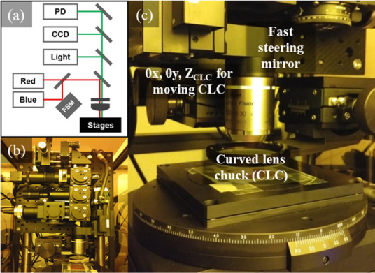
Image of a laser diode-based optic system. (a) Conceptual system. (b) Full view of the system (450 × 450 × 520 mm3). (c) X, Y, ZOL, and rotation stages that align the substrate and θx, θy, and another ZCLC stage that align LEDs.
Repeated contact between the LED and the substrate may increase the chance that the LED will be damaged or contaminated. To overcome these problems, a CLC with a constant radius of curvature (R = 180 mm) was used so that each LED can successively contact the substrate (Figure 2c). Furthermore, manual swivel (θx and θy) stages and a manual vertical translation (ZCLC) stage were integrated to align the LED. The travel distance of the θx and θy stages was ±2.56 mm (R = 180 mm), and the stroke of the ZCLC stage was 13 mm.
The system had an illumination (λ = 730 nm) for a charge-coupled device (CCD) camera for real-time monitoring of the process. The effective pixel number of the CCD camera was 768 (H) × 494 (V), and the unit cell size was 8.4 × 9.8 μm2. For accurate and precise positioning of the process beam, it can be positioned via a laser with a wavelength that does not affect the UV release tape. For this reason, a red laser diode (λ = 660 nm, max power = 120 mW, Hitachi, HL6501MG) was used. The wavelength of the process beam was 375 nm (laser diode, max power = 70 mW, Nichia, NDU4116). The laser diode was characterized by a divergent beam. For utilization, the divergent beam must, therefore, be collimated and then focused again by an objective lens (OL; N.A. = 0.3, W.D. = 30 mm, focal length = 10 mm, Nikon, MUE31200), with a motorized vertical translation (ZOL) stage. The stroke of the ZOL stage was 30 mm, the resolution was 100 nm, the repeatability was ±300 nm, and the maximum speed was 10 mm/s. The OL is a super-long working distance type used to avoid collision with the CLC during selective transfer.
After aligning the LED via the donor and acceptor stages, the CCD camera with illumination, and the focused red laser diode, the LED was irradiated by the process beam. To selectively transfer LEDs onto the UV release tape, only the beam as much as the LED size should be irradiated. However, the focused beam should be scanned as its size (<2 um) is very small compared to the LED beam; despite this, selective transfer using scanning does not require prior preparation according to the LED size.
The scanning stage is inefficient owing to the limitations of mechanical acceleration and deceleration. To overcome this, a fast steering mirror (FSM; Newport, FSM-300) was used. The FSM has a small angle tilt (±26 mrad) and can thus drive a few kilohertz within the field of view of the OL. The FSM is operated according to the following equation, which generates a Lissajous pattern
| 1 |
where A and B are amplitudes [μm], a and b are frequencies [Hz], t is time [s], and δ is the phase difference. Figure 3 shows the MATLAB simulations for the optimization of the beam trajectory produced by the FSM. Figure 3a,b shows the simulation results of a focused beam as a simple spot with a diameter of 2 μm so that the path through which the beam passes can fill an almost uniform area within a given time. The simulation results showed that the most suitable process conditions for filling a specific area are A = 240 μm, B = 120 μm, a = 97 Hz, b = 93 Hz, t = 0.5 s, δ1 = 0, and δ2 = π/4. Figure 3c,d shows the simulation results of the focused beam as a Gaussian beam. An excessive concentration of energy is observed near the edge. Figure 3e,f shows the results of the energy distribution along the X and Y axes. The process results are affected; the concentration of energy in the edge region naturally occurs in Lissajous scanning based on sine waves, and it is thought that a lot of energy will accumulate in the edge region when irradiated with a laser beam in the same area as the size of the LED device. This paper attempts to determine the process conditions by uniformly irradiating the appropriate light energy to all areas where the donor substrate and LED are in contact with each other. The laser beam was thus irradiated to an area 20% larger than the LED size.
Figure 3.

MATLAB simulation results to determine optimal conditions. (a) Hypothesizing that the intensity of a beam is constant. (b) Optimal condition for eq 1. (c) Assuming that the intensity of the beam is the Gaussian intensity. (d) Energy concentration verified at the edges. Energy distribution graphs along the (e) X axis and (f) Y axis.
In this experiment, we used two LEDs with different wavelengths and sizes to show that the proposed system can perform the transfer, regardless of the LED size (Figure 4). Figure 5 shows a detailed sequence of the selective transfer. A UV-curable adhesive (NOA84, Norland) was spin-coated onto a flexible printed circuit board (FPCB) as an acceptor substrate (Figure 5a,b). There are two types of FPCBs: one for a 200 μm long green LED and the other for a 300 μm long red LED. The full FPCB size for the green LED was 16.5 × 30 mm2, the metal pad size was 300 × 200 μm2, and the pad spacing was 450 μm. The full FPCB size for the red LED was 20 × 50 mm2, the metal pad size was 300 × 800 μm2, and the pad spacing was 650 μm.
Figure 4.

SEM images. (a) Green LED (λ = 530 nm, size = 200 × 100 × 100 μm3) and (b) red LED (λ = 620 nm, size = 300 × 100 × 100 μm3).
Figure 5.

Illustration of a detailed sequence of selective transfer. (a, b) Adhesive layer via spin-coating on an FPCB as an acceptor substrate. (c, d) Placing LEDs on a substrate via focused laser scanning. (e) Removing the adhesive layer on the pads for interconnection. (f) Depositing a few drops of the conductive material.
The UV release tape with the LED array lifted from the sapphire substrate should be precured because the adhesion force is too strong. Precuring was conducted for the UV release tape using an LED array lamp (λ = 405 nm, power = 100 mW/cm2) for 30 s. When precuring at an i-line wavelength, the energy absorption rate of the UV release tape was so good that the adhesion force decreased sharply, which was difficult to control. Therefore, the UV release tape with the LED was precured at a wavelength of 405 nm. The adhesive layer thickness of the UV release tape (SM Technology, DU-115P) was 15 μm, and the adhesive forces before and after UV irradiation were 2150 and 20 gf/25 mm, respectively. After aligning with the LED and metal pad, UV irradiation was applied to the contact surface of the URT and LED (Figure 5c,d). The adhesive layer on the metal pad was then removed for interconnection, completing the selective transfer of the LED (Figure 5e). For the interconnection between the metal and LED pad, several drops of a conductive silver paste (CANS ELCOAT, P-100) were dropped and then naturally dried (Figure 5f).
Results and Conclusions
The proposed process is conducted by appropriately controlling the five forces. Table 1 summarizes the understanding of the force correlations used in this experiment.
Table 1. Correlation of Forces.

We confirmed that an LED can only be transferred when the adhesion force of the UV-curable adhesive is stronger than that of the UV release tape (F3 > F4). The average (Avg) and standard deviation (SD) of the alignment errors between the LED and FPCB were as follows: XAvg = 23.57 μm, XSD = 19.59 μm, YAvg = 24.64 μm, YSD = 21.96 μm, θAvg = 2.66°, and θSD = 2.47°.
The first factor in the alignment error is the assembly misalignment of ZCLC and ZOL. Second, as the moment when the LED and FPCB coming into contact is verified with the CCD camera, it is difficult to quantify the contact force. Moreover, as the stages for aligning the CLC are operated manually, it seems that these problems are compounded to cause alignment errors.
Figure 6 shows that LEDs can be transferred selectively to five locations on the FPCB for a green LED. The FPCB connection platform with resistance regulation and a 5 V DC power supply was customized. The transfer process in this study is more flexible than the simple matrix arrangement or pick-and-place methods. To verify this, we selectively transferred 13 LEDs from an array of LEDs on a UV release tape to a flexible substrate one-by-one; it was confirmed that LEDs were undamaged and uncontaminated during the transfer by turning on LEDs via interconnecting the LEDs and the flexible substrate (Figure 7). Through this experiment, it was confirmed that the proposed system and process can be used to place LEDs by controlling the position (360°) regardless of the angle of the LED. The interconnection was performed using a simple method, and the problem of cracking in the conductive material (silver paste) was confirmed when a continuous banding test was conducted, as shown in Figures 6 and 7. In future studies, high-level interconnection technology is expected to be required.
Figure 6.

Transferred five green LEDs onto a 5 × 5 array FPCB and the full size is 16.5 × 30 mm2.
Figure 7.

Transferred 13 red LEDs onto a 5 × 5 array clock-like FPCB and the full size is 20 × 50 mm2.
The proposed transfer has two advantages. First, it is independent of changes in the adhesive force of the donor substrate. Second, LED transfer occurs via laser scanning onto the donor substrate (UV release tape) so that the laser scanning area can be changed immediately depending on the LED size.
Various studies utilizing smaller LED sizes are currently underway. However, as the thickness of LED decreases, the thickness of the adhesive layer of the UV release tape becomes significant. If the thickness of the UV release tape is thicker than the LED, then the LED is buried in the adhesive layer of the UV release tape. In the future, it would be appropriate to apply it to the selective transfer process via a UV release tape with an adhesive layer (submicrometer) thinner than the thickness of the LED.
We transferred LEDs via scanning methods owing to their various sizes. If the LED size is fixed, then the processing time would be more effective via a beam-shaping method. The smaller the sizes of LEDs, the more LEDs we will have to individually deal with. We expect that the proposed transfer can replace parts that are difficult to transfer via conventional technologies, such as pick-and-place or large-area transfer. In particular, there could be defective micro-LEDs after a large-scale transfer in a micro-LED display field; our process will help conduct repairs.
Acknowledgments
The authors thank the Ministry of Science and ICT (MSIT) of Korea as the original technology development project for nanomaterials and the BioNano Health-Guard Research Center, and this work was funded by the Ministry of Science, ICT and Future Planning of the Korea government (grant nos. 2017M3A7B4041754 and H-GUARD_2013M3A6B2078).
The authors declare no competing financial interest.
References
- Guan N.; Dai X.; Messanvi A.; Zhang H.; Yan J.; Gautier E.; Bougerol C.; Julien F. H.; Durand C.; Eymery J.; Tchernycheva M. Flexible white light emitting diodes based on nitride nanowires and nanophosphors. ACS Photonics 2016, 3, 597–603. 10.1021/acsphotonics.5b00696. [DOI] [PMC free article] [PubMed] [Google Scholar]
- Lee H. E.; Shin J. H.; Park J. H.; Hong S. K.; Park S. H.; Lee S. H.; Lee J. H.; Kang I.-S.; Lee K. J. Micro Light-Emitting Diodes for Display and Flexible Biomedical Applications. Adv. Funct. Mater. 2019, 29, 1808075. 10.1002/adfm.201808075. [DOI] [Google Scholar]
- Xu L.; Gutbrod S. R.; Bonifas A. P.; Su Y.; Sulkin M. S.; Lu N.; Chung H.-J.; Jang K.-I.; Liu Z.; Ying M.; Lu C.; Chad Webb R.; Kim J.-S.; Laughner J. I.; Cheng H.; Liu Y.; Ameen A.; Jeong J.-W.; Kim G.-T.; Huang Y.; Efimov I. R.; Rogers J. A. 3D multifunctional integumentary membranes for spatiotemporal cardiac measurements and stimulation across the entire epicardium. Nat. Commun. 2014, 5, 1–10. 10.1038/ncomms4329. [DOI] [PMC free article] [PubMed] [Google Scholar]
- Goßler C.; Bierbrauer C.; Moser R.; Kunzer M.; Holc K.; Pletschen W.; Köhler K.; Wagner J.; Schwaerzle M.; Ruther P. GaN-based micro-LED arrays on flexible substrates for optical cochlear implants. J. Phys. D: Appl. Phys. 2014, 47, 205401. 10.1088/0022-3727/47/20/205401. [DOI] [Google Scholar]
- Lee H. E.; Lee D.; Lee T.-I.; Shin J. H.; Choi G.-M.; Kim C.; Lee S. H.; Lee J. H.; Kim Y. H.; Kang S.-M.; Park S. H.; Kang I.-K.; Kim T.-S.; Bae B.-S.; Lee K. J. Wireless powered wearable micro light-emitting diodes. Nano Energy 2019, 55, 454–462. 10.1016/j.nanoen.2018.11.017. [DOI] [Google Scholar]
- Chun J.; Hwang Y.; Choi Y.-S.; Kim J.-J.; Jeong T.; Baek J. H.; Ko H. C.; Park S.-J. Laser lift-off transfer printing of patterned GaN light-emitting diodes from sapphire to flexible substrates using a Cr/Au laser blocking layer. Scr. Mater. 2014, 77, 13–16. 10.1016/j.scriptamat.2014.01.005. [DOI] [Google Scholar]
- Choi W.-S.; Park H. J.; Park S.-H.; Jeong T. Flexible InGaN LEDs on a polyimide substrate fabricated using a simple direct-transfer method. IEEE Photonics Technol. Lett. 2014, 26, 2115–2117. 10.1109/LPT.2014.2348591. [DOI] [Google Scholar]
- Kim J.; Kim J.-H.; Cho S.-H.; Whang K.-H. Selective lift-off of GaN light-emitting diode from a sapphire substrate using 266-nm diode-pumped solid-state laser irradiation. Appl. Phys. A: Mater. Sci. Process. 2016, 122, 305. 10.1007/s00339-016-9928-7. [DOI] [Google Scholar]
- Kim B. H.; Nam S.; Oh N.; Cho S.-Y.; Yu K. J.; Lee C. H.; Zhang J.; Deshpande K.; Trefonas P.; Kim J.-H.; Lee J.; Shin J. H.; Yu Y.; Lim J. B.; Won S. M.; Cho Y. K.; Kim N. H.; Seo K. J.; Lee H.; Kim T. i.; Shim M.; Rogers J. A. Multilayer transfer printing for pixelated, multicolor quantum dot light-emitting diodes. ACS Nano 2016, 10, 4920–4925. 10.1021/acsnano.5b06387. [DOI] [PubMed] [Google Scholar]
- Sharma B. K.; Jang B.; Lee J. E.; Bae S. H.; Kim T. W.; Lee H.-J.; Kim J. H.; Ahn J.-H. Load-Controlled Roll Transfer of Oxide Transistors for Stretchable Electronics. Adv. Funct. Mater. 2013, 23, 2024–2032. 10.1002/adfm.201202519. [DOI] [Google Scholar]
- Seo J.-H.; Li J.; Lee J.; Gong S.; Lin J.; Jiang H.; Ma Z. A simplified method of making flexible blue LEDs on a plastic substrate. IEEE Photonics J. 2015, 7, 1–7. 10.1109/JPHOT.2015.2412459. [DOI] [Google Scholar]
- Cok R. S.; Meitl M.; Rotzoll R.; Melnik G.; Fecioru A.; Trindade A. J.; Raymond B.; Bonafede S.; Gomez D.; Moore T.; Prevatte C.; Radauscher E.; Goodwin S.; Hines P.; Bower C. A. Inorganic light-emitting diode displays using micro-transfer printing. J. Soc. Inf. Disp. 2017, 25, 589–609. 10.1002/jsid.610. [DOI] [Google Scholar]
- Huang Y.; Zheng N.; Cheng Z.; Chen Y.; Lu B.; Xie T.; Feng X. Direct laser writing-based programmable transfer printing via bioinspired shape memory reversible adhesive. ACS Appl. Mater. Interfaces 2016, 8, 35628–35633. 10.1021/acsami.6b11696. [DOI] [PubMed] [Google Scholar]
- Yoo B.; Cho S.; Seo S.; Lee J. Elastomeric angled microflaps with reversible adhesion for transfer-printing semiconductor membranes onto dry surfaces. ACS Appl. Mater. Interfaces 2014, 6, 19247–19253. 10.1021/am505286b. [DOI] [PubMed] [Google Scholar]
- Park S.-I.; Xiong Y.; Kim R. H.; Elvikis P.; Meitl M.; Kim D.-H.; Wu J.; Yoon J.; Yu C. J.; Liu Z.; Huang Y.; Hwang K.-C.; Ferreira P.; Li X.; Choquette K.; Rogers J. A. Printed assemblies of inorganic light-emitting diodes for deformable and semitransparent displays. Science 2009, 325, 977–981. 10.1126/science.1175690. [DOI] [PubMed] [Google Scholar]
- Choi M.; Jang B.; Lee W.; Lee S.; Kim T. W.; Lee H.-J.; Kim J.-H.; Ahn J.-H. Stretchable active matrix inorganic light-emitting diode display enabled by overlay-aligned roll-transfer printing. Adv. Funct. Mater. 2017, 27, 1606005. 10.1002/adfm.201606005. [DOI] [Google Scholar]
- Kim T.-i.; Lee S. H.; Li Y.; Shi Y.; Shin G.; Lee S. D.; Huang Y.; Rogers J. A.; Yu J. S. Temperature- and size-dependent characteristics in ultrathin inorganic light-emitting diodes assembled by transfer printing. Appl. Phys. Lett. 2014, 104, 051901 10.1063/1.4863856. [DOI] [Google Scholar]
- Carlson A.; Bowen A. M.; Huang Y.; Nuzzo R. G.; Rogers J. A. Transfer printing techniques for materials assembly and micro/nanodevice fabrication. Adv. Mater. 2012, 24, 5284–5318. 10.1002/adma.201201386. [DOI] [PubMed] [Google Scholar]