

Abstract
An eight-channel readout ASIC has been developed for reading output signals from solid-state photomultipliers for positron emission tomography applications. This ASIC converts both the signal charge and occurring time to digital timing pulses so that only a time-to-digital converter is required for further signal processing. This provides the advantages of simplified circuit design, reduced power consumption, and suitability for applications that have a large number of readout channels. The ASIC uses a fully current mode preamplifier to achieve high bandwidth (> 100 MHz), high time resolution (better than ~1 ns FWHM), and low power consumption (a few mW/ch). The linear dynamic range of charge measurement is adjustable and can be extended up to 103 pC. The chip has been fabricated with 0.35 μm 2P4M CMOS technology. A test prototype board has been developed and used for ASIC functionality and performance evaluation. Our preliminary studies show that the targets have been successfully achieved.
Index Terms: Application-specific integrated circuits, nuclear electronics, positron emission tomography
I. Introduction
Solid-state photo multipliers (SSPMs) have gained popularity in recent years as the choice of scintillation photon sensors for nuclear medicine instruments and other radiation detector applications [1]–[4]. Compared with PMT and avalanche photodiodes (APDs), SSPMs combine the advantages of compact size, high amplification gain (~106), fast signal rising time (achievable within 1 to 10 ns), and low bias voltage. In addition, they are immune to magnetic fields, making them suitable for combined positron emission tomography (PET) and magnetic resonance imaging (MRI) applications [5], [6].
However, because of its high granularity, an SSPM array may require the use of high-density readout electronics, with a large number of readout channels, in some practical radiation detector designs. For a PET detector, the signal charge (energy information) and occurring time of a gamma interaction need to be measured. Conventionally, the front-end readout electronics of a PET detector has an amplifier-shaper-discriminator structure, and the signal charge and timing are processed separately by an analog-to-digital converter (ADC) and a time-to-digital converter (TDC). A constant fraction discriminator (CFD) is usually needed for higher timing accuracy. Several such application-specific integrated circuit (ASIC) readout chips have been developed for avalanche photodiode- or SSPM-based PET detectors [7]–[11]. However, the drawbacks of such conventional designs are high circuit complexity and difficulty in implementing high-quality, adjustable on-chip delay lines for CFD. Recently, various designs with time-based readouts (TBRs) have been explored in which the signal charge is converted to a timing interval at the front-end level so that only a TDC is needed to process the signal charge and timing signals. This approach greatly simplifies the entire signal processing chain at the system level, and whilst multi-channel, sub-nanosecond-resolution, field-programmable gate array (FPGA)-based TDCs have become readily available [12], [13]. Different charge-to-time convertor (QTC) methods have already been proposed and studied. For example, the time over threshold (TOT) may be the easiest to implement, although its conversion is intrinsically non-linear [14]. A multi-level or dynamic TOT method has been proposed to improve the non-linearity [15], [16]. Other approaches, such as pulse-width modulation, have also been proposed [17], [18].
We have recently proposed and evaluated a new method to further simplify the design and improve performance: 1) a leading edge discriminator is used to pick off the signal timing, and the measured signal amplitude can be used to correct the time-walk errors. Therefore, no CFD is needed in this TBR design. 2) An alternative QTC method based on the Wilkinson discharging principle was developed to further improve the accuracy and stability of signal measurement [19]. It provides excellent linearity, with the discharging time controlled by a fixed current source that is proportional to the quantity of the integrated input charge. This circuit is described in Section II.
A TBR front-end ASIC (named TIMPIC ASIC for TIMe PICk off) with the new method has been developed. It has several key features: 1) a current mirror input stage is adopted instead of a traditional charge-sensitive preamplifier; 2) the charge integration is performed by a gated integrator, and the gate signal is generated by the timing discriminator; and 3) the input current is only integrated when it presents; thus, the integrated noise charge can be minimized, especially for detectors with high dark-count rates such as SSPMs. A detailed circuit design and analysis is presented in Section III. The test results are described in Section IV.
II. Architecture and Specifications
A. QTC Principle
The principle of the new QTC is shown in Fig. 1. The input current signal arrives at T0 and triggers the current discriminator at T1. The output of the current discriminator (TT) is then used as a gate signal for charge integration. An attenuated copy of the input current signal is integrated onto a capacitor when TT is high A poly-insulator-poly capacitor is used for its low temperature coefficient and low leakage current. The attenuation factor of the current mirror can be properly chosen for a large-input dynamic range.
Fig. 1.
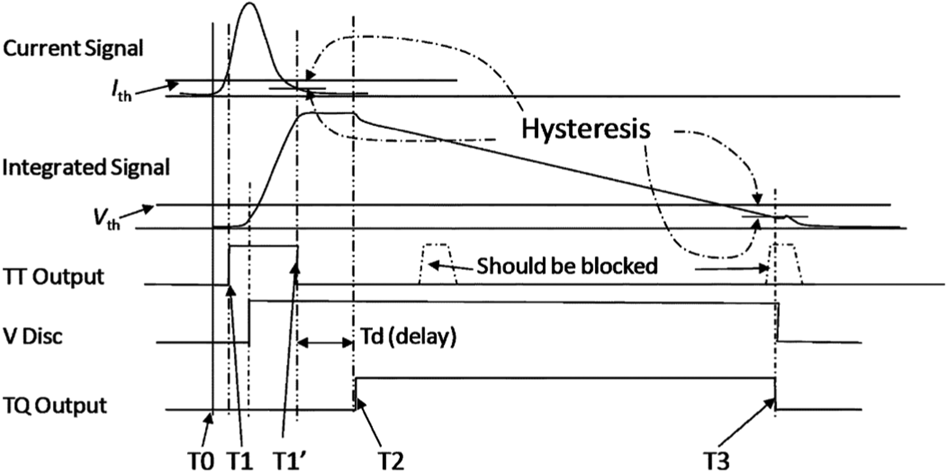
The principle of TBR-based signal and timing measurement with a new QTC design.
After the integration is over, the capacitor starts to discharge at T2 through a constant current circuit until the voltage on the capacitor drops to the lower threshold of a voltage discriminator at T3. The discharge time TQ = T3 – T2 is then proportional to the signal charge.
Two major causes of potential non-linearity exist. First, the gate width changes with the signal amplitude, e.g., the time-walk effect. Only signal components above the threshold will be integrated; thus, the smaller signal may lose a larger partition of its total charge. Second, the input current buffer and discharging current source have limited output resistances. The charging and discharging currents may change with the voltage on the capacitor. Nevertheless, these high-order effects can be suppressed using appropriate circuit parameters (e.g., the current threshold and transistor length).
The major noise sources that degrade the charge measurement resolution are thermal electronic noise, detector dark-count noise, and charge-dependent time width variation (T3 – T2). Overall, the signal charge measurement resolution can be written as:
Where is the thermal noise from the input attenuation stage; M is the dark count rate; Qdark is the integrated charge for a single dark count; is the thermal noise from the discharging current source; Tint and Tdis are the integration time and discharging time, respectively; σv,cpm is the equivalent noise voltage of the voltage comparator; Cint is the integration capacitance; σTDC is the time resolution of the TDC; Idis is the discharging current; and a1, a2, and a3 are the noise coefficients, depending on the corresponding noise or signal bandwidth.
The first three terms are proportional to the integration gate width and discharging time: 200–400 ns (for LYSO scintillator) and ~1μs, respectively. The dark-count noise from the SSPM detector usually dominates in the overall noise. A charge variance of a few pC could be contributed for typical dark count rate values versus ~1 fC from the thermal noise of the circuits. Voltage comparator noise may also make significant contributions because of a large capacitor used for integration. The contribution of the TDC is proportional to the discharging current and thus inversely proportional to the maximum discharging time. The charge variance caused by the voltage comparator and TDC is 10–100 fC. Trade-off is required among the charge resolution, count rate capability, and TDC resolution for different application needs.
B. SSPM Characteristics
The SSPM used in this study is a 4 × 4 SSPM array (SensL SPMArray4) with a 15.31 × 15.81 mm2 outline dimension and a 3.17 × 3.17 mm2 area for each SSPM pixel element. Detailed electrical and mechanical parameters can be found on the manufacturer’s website [20]. The key parameters that determine the main ASIC design specifications include
— ~2 × 10⁶ gain at a bias voltage of ~32 V.
— 8 MHz dark count rate of each pixel.
— 25 ns intrinsic current rise time constant.
The slow rise time can be observed directly with an oscilloscope and is mainly limited by the parasitic resistance of the package (about 100 Ohm) and detector capacitance. The typical output signal of a 511 keV photo-peak interaction measured from a SSPM optically coupled to a 2 × 2 × 20 mm3 LYSO scintillator yielded about a 5 mA peak current and around 250 pC total charge.
C. Chip Architecture and Specifications
A block diagram of a one-channel circuit is shown in Fig. 2. It consists of an input current mirror stage with two output branches: one for the timing discriminator and the other for charge integration and measurement. The control logic for charge-to-time conversion is determined by the control logic module. Each channel has two outputs: TT and TQ. TT is the direct output of the current discriminator, and its rising edge corresponds to T1. TQ is the output of the control logic, and its width is proportional to the signal charge.
Fig. 2.
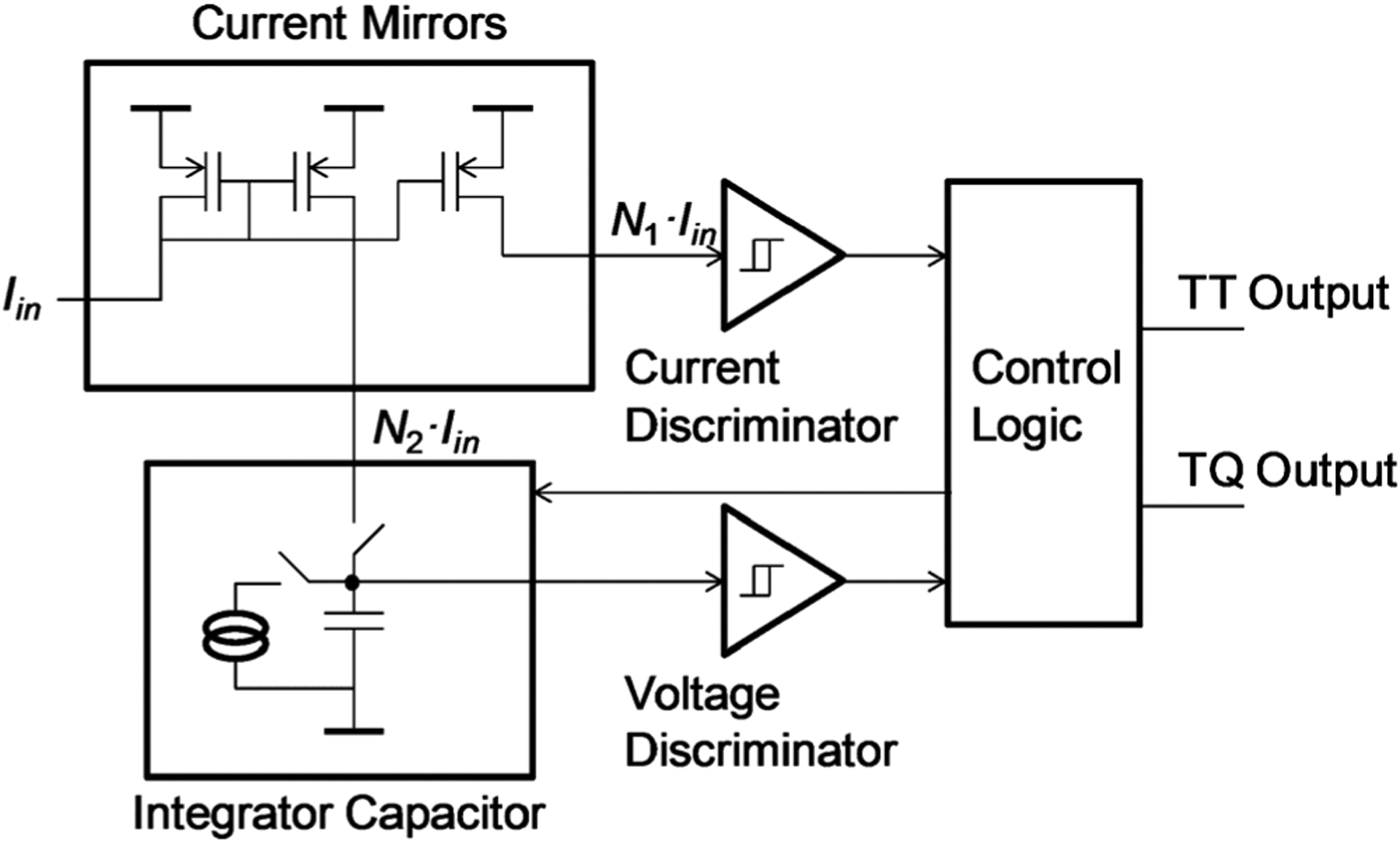
Block diagram of a one-channel circuit. The circuit consists of an input current mirror stage with two output branches: one for the timing discriminator and the other for charge integration and measurement. Therefore, each channel has two outputs: TT and TQ. The logical signals for charge to time conversion are generated by the control logic module.
The design specifications of the ASIC are defined and summarized in Table I.
TABLE I.
Design Specifications of the TIMPIC Chip
| Parameter | Performance |
|---|---|
| Input charge range | Up to 1000 pC |
| INL | Better than +/−1 % for 10:1 range |
| Bandwidth | 100 MHz |
| Input impedance | 50 Ω |
| Discriminator type | Leading edge |
| Time resolution ~1 ns, FWHM | |
| Power consumption | < 10 mW/ch |
| Number of channels | 8 |
| Technology | CMOS 0.35 μm process |
III. Circuit design and Analysis
A. Input Stage
A full-current mode circuit has been designed for the input stage (i.e., using currents to represent the signal information instead of node voltages). A simplified circuit schematic is shown in Fig. 3.
Fig. 3.
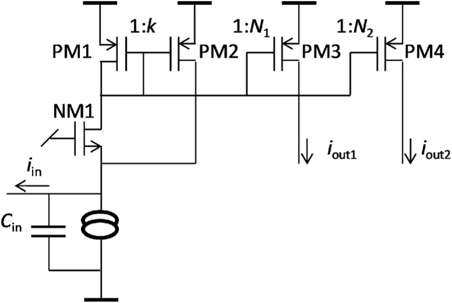
A simplified schematic of the input stage.
The input stage consists of two current mirrors: one for the timing discriminator (PM1–PM3) and the other for charge integration (PM1–PM4). The key design parameters for the current mirrors are the input impedance and the bandwidth. To achieve low input impedance, a common gate NMOS transistor (NM1) is inserted between the input and the current mirror. A current feedback through PM2 is also adopted, and the input impedance can be reduced by a factor of (1 + κ). However, special care is needed for stability. The dominant pole at the input node is –gm,n1/Cin, and the second pole at the PM1–PM4 gates is –gm,p1/(Cgs,p1 + Cgs,p2 + Cgs,p3 + Cgs,p4). It is important to separate the two poles with proper layout sizes and biases of NM1 and PM1–PM2 transistors.
B. Current Discriminator
A simplified circuit schematic of the current discriminator is shown in Fig. 4.
Fig. 4.
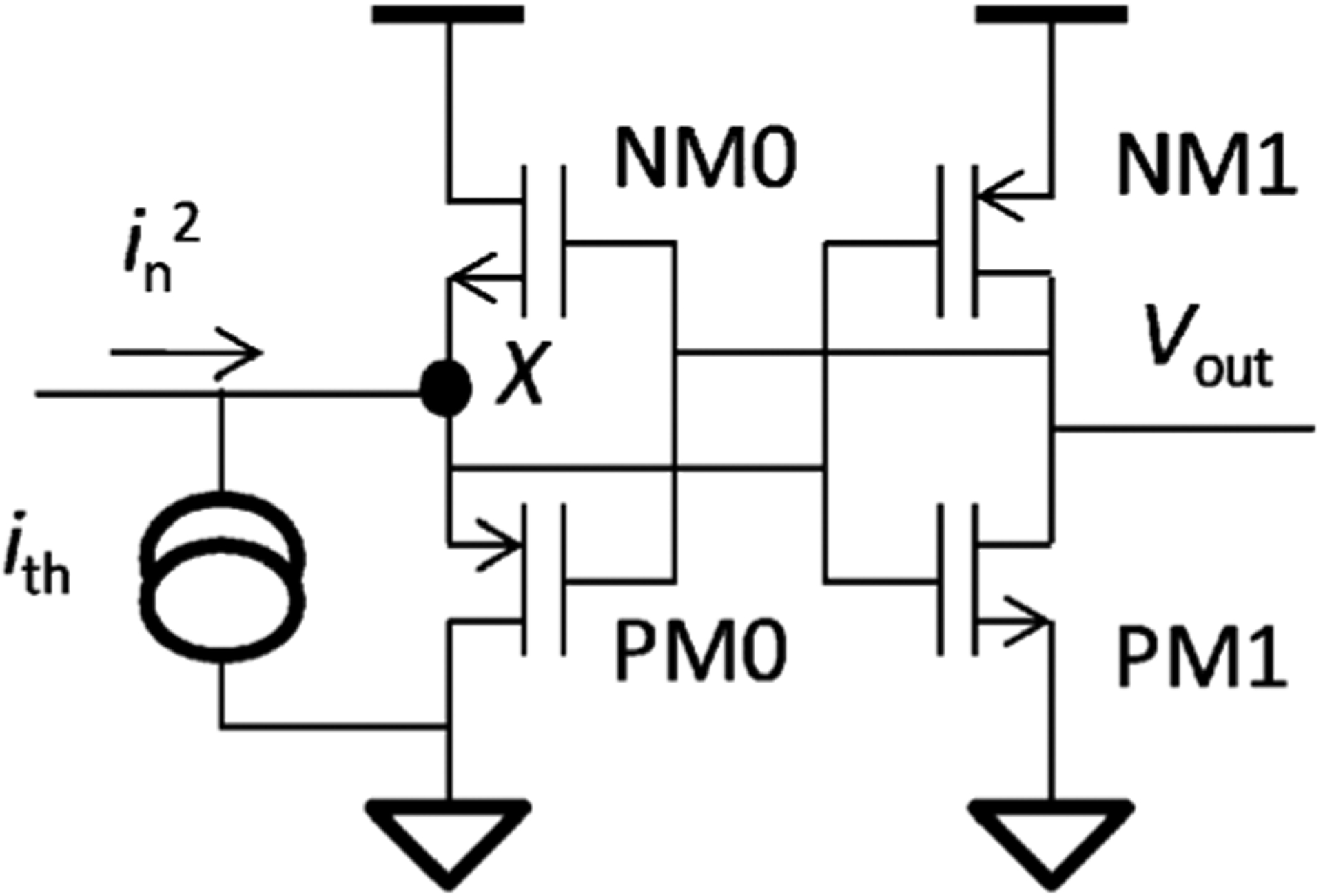
A simplified circuit schematic of the current discriminator.
The output state is determined by the voltage of the input node X, and the time response of the discriminator is dependent on the speed of the input signal that charges or discharges the parasitic capacitor at the input. Because the parasitic capacitance is small, fast transition speed and good timing performance can be achieved. The complete discriminator circuit includes an adjustable hysteresis circuit to avoid oscillation.
C. QTC Circuit
The QTC circuit consists of a switched capacitor, a discharging current source, a voltage discriminator, and a control logic module. No charge-sensitive preamplifier or shaper circuits are needed. The static power consumption is almost zero except for the input stage of the voltage discriminator. The signal current is attenuated; thus, the maximal charge of 1000 pC can be measured with an on-chip capacitor.
When the current discriminator is triggered, the integration capacitor is switched on and the attenuated copy of the input current starts to charge the capacitor until the current discriminator output drops. The voltage on the capacitor increases and may trigger the voltage discriminator. After a certain time delay that is implemented by a starved inverter, a fixed current source starts to discharge the capacitor until the voltage discriminator output turns off. An output pulse is generated, with a width corresponding to that of the discharging time.
D. Chip Layout and Package
The layouts of one-channel circuits and the whole chip are shown in Fig. 5(a) and (b). The one-channel circuit area is 100 × 1200 μm2, and the whole chip is 2.35 × 2.35 mm2. The chip is bonded on a CLCC68 package (25 × 25 mm2) for testing, as shown in Fig. 6(a). It can be directly bonded on a PCB and mounted as closely as possible to the detector for a more compact design. A specially designed PCB has been built for TIMPIC performance evaluation (Fig. 6(b)). This board allows us to test a selected channel or simultaneously test all channels. A SSPM array (SensL SPMArray4) with 4 × 4 pixels can be tested with 2 TIMPIC ASICs on this set-up.
Fig. 5.
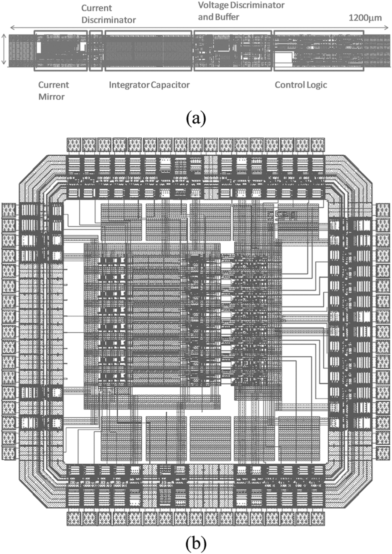
Chip layout. (a) One-channel circuit, 100 × 1200 μm2; (b) the chip, 2.35 × 2.35 mm2.
Fig. 6.
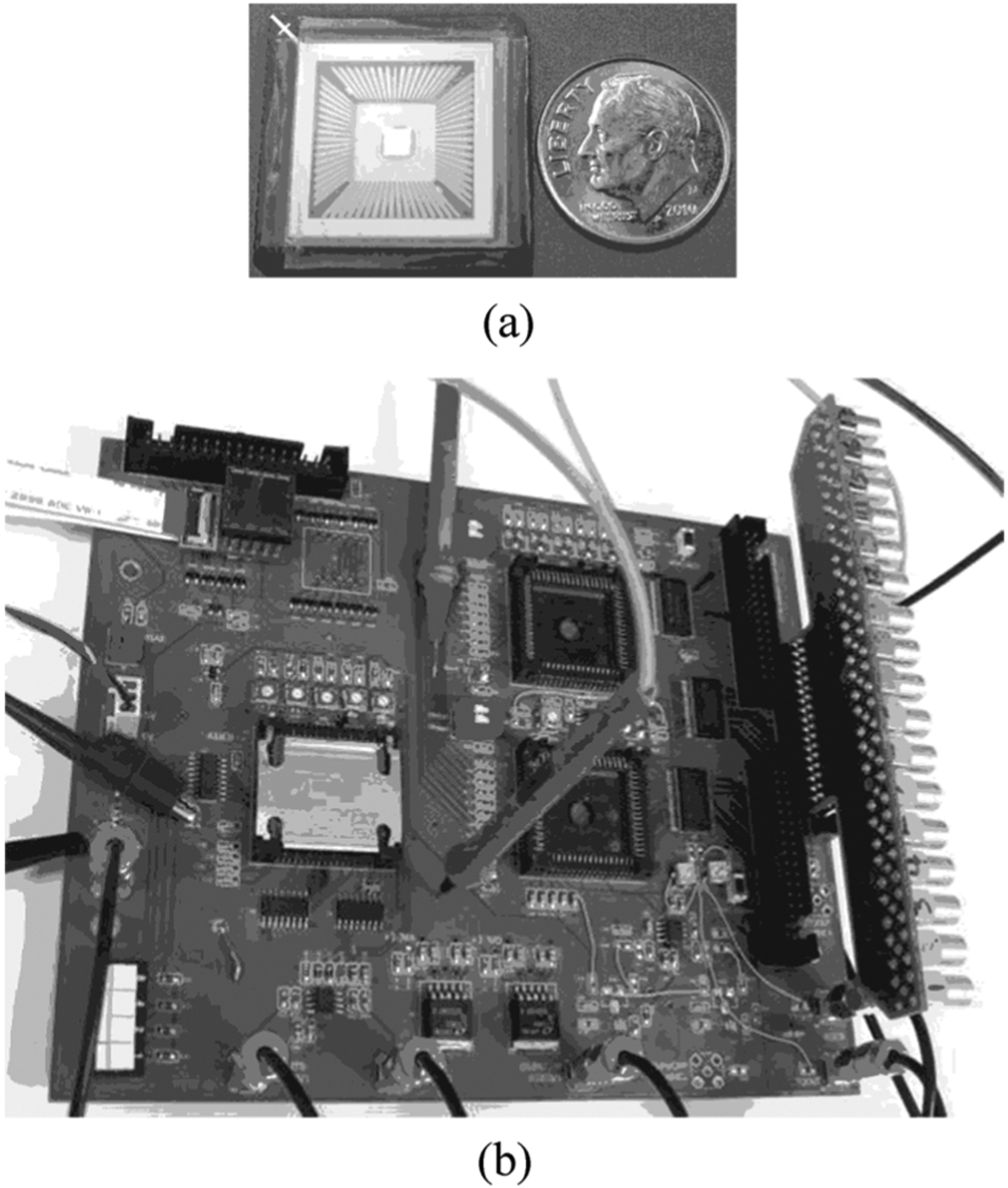
Packaged ASIC and test PCB. (a) Packaged TIMPIC ASIC chip; (b) Test board for ASIC performance evaluations.
IV. Test Results
A. Static Performance
The circuit bias current can be adjusted using a master bias resistor for all 8 channels. The bias current ranged from 6.5 to 100 μA. Power consumption was measured at different bias conditions, as shown in Fig. 7. The lower system bias current provides a larger dynamic range. Thus, a 10–20 μA bias has been used for the most of the following tests, with the power consumption less than 5 mW per channel. The static input impedance is less than 50 Ω and is related to the gate bias voltage and the current of the NM1, as shown in Fig. 3.
Fig. 7.
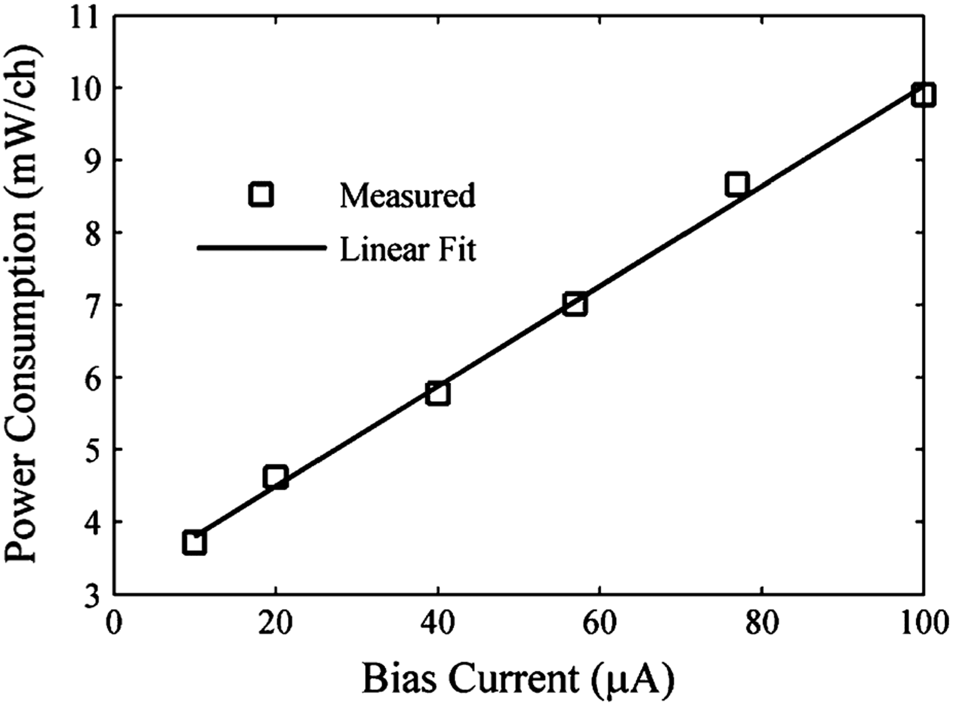
Power consumption of the ASIC chip with different bias conditions. We chose a bias current of 20 μA for most tests, and the power consumption was less than 5 mW per channel.
B. QTC Functionality Test
The ASIC chip was tested using current pulses injected from a signal generator. The waveforms were recorded and are shown in Fig. 8. They correspond to:
Fig. 8.
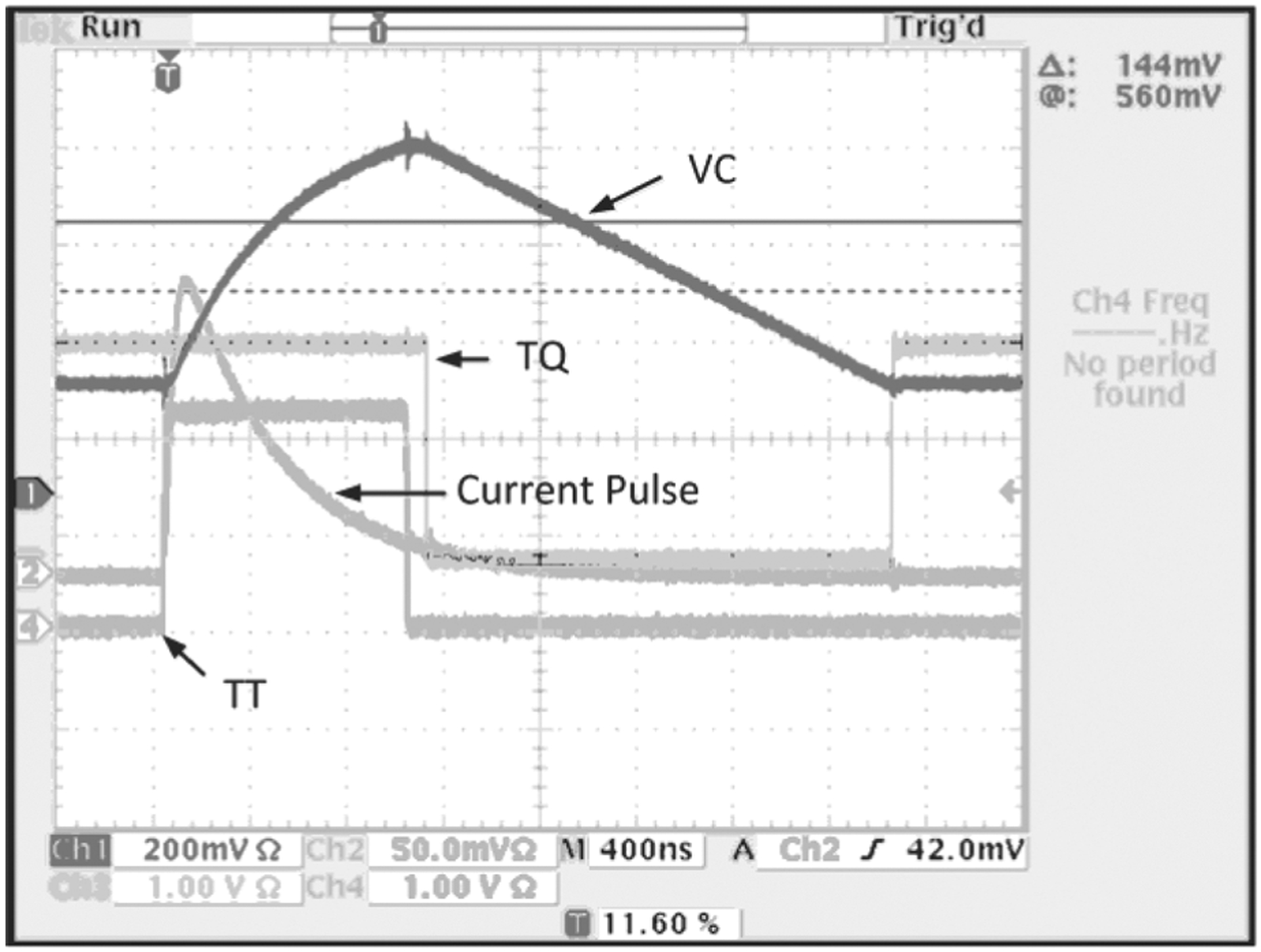
Transient waveforms recorded for functionality tests: Current pulse: the input current signal; TT: timing output signal; TQ: QTC output signal; VC: the voltage on the integration capacitor.
— Current Pulse: the input current pulse that mimics the detector output signal
— TT: the current discriminator output signal for timing measurement
— TQ: the QTC output for charge measurement
— VC: the voltage on the integration capacitor.
The timing discriminator output (TT) rises immediately after the current signal begins and falls back to the ground when the signal level decays below the threshold. The pulse width is dependent on the current shape and amplitude at some level. It is used as a gate signal for charge integration. The monitored voltage on the integration capacitor increases during this time. The linear discharging process can also be clearly seen. There is around a 80-ns delay between integration and discharge. The pulse width of TQ exactly equals the discharging time.
The TT and TQ were designed with the CMOS logic standard. The rise and fall time are less than 6 ns, with 50-Ω load in parallel and a 50-pF capacitor. The output signal magnitude of logic high is above 2.5 V.
C. QTC Performances: Linearity and Accuracy
The linearity and dynamic range of the QTC were measured with the square and double-exponential current pulses by the signal generator. The square current pulse was used to calibrate the circuit and investigate the non-linearity caused by the output resistance of the current mirror and discharging current source. We chose a 100-ns square current width for simplicity. The double-exponential pulses were used to mimic SSPM output signals so the linearity performance study could more closely approximate a real gamma ray detecting situation.
The measured results with their linear fits are shown in Fig. 9. Different discharging current rates were used. INL (integral non-linearity) was less than 0.8% for square signals and less than 0.57% for double-exponential signals from 100 to 1000 pC.
Fig. 9.
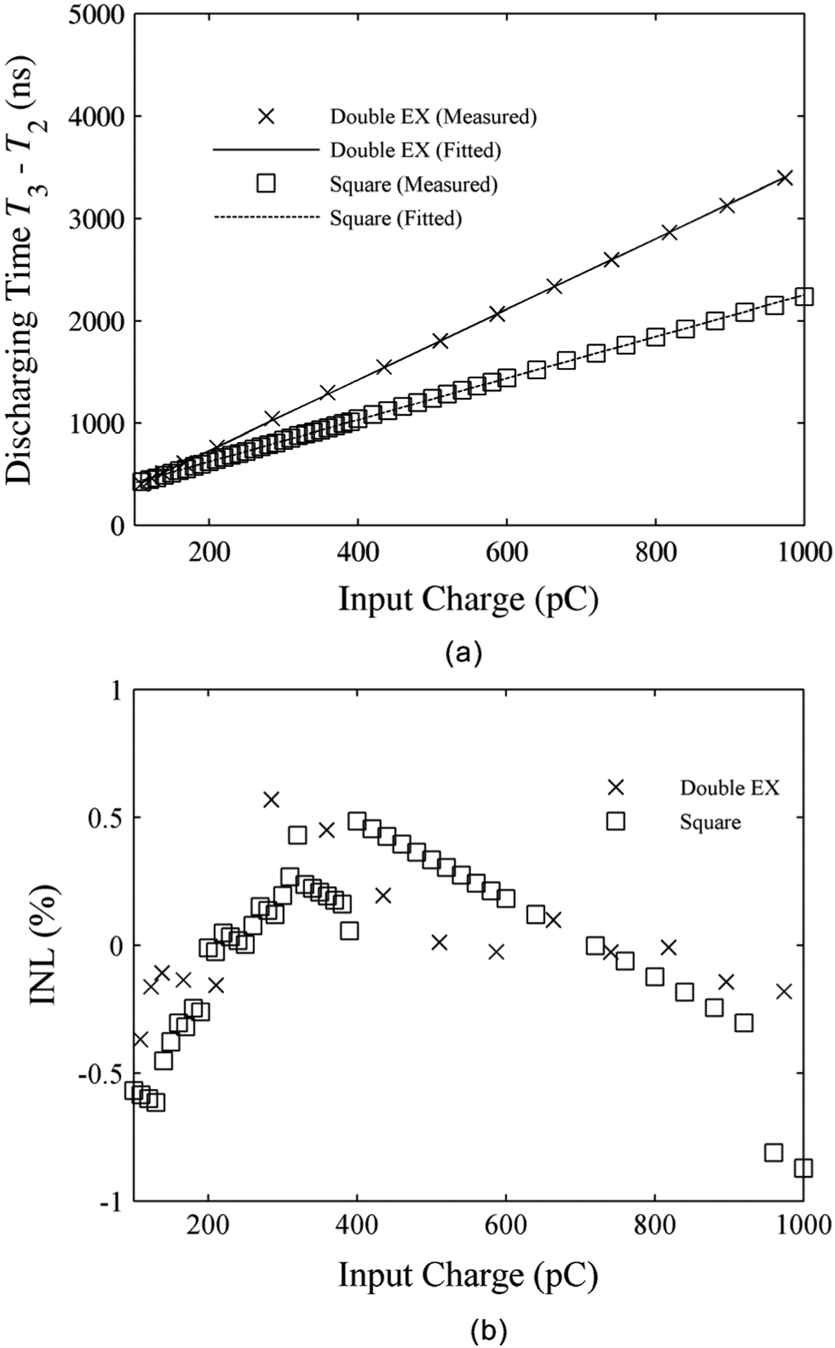
Linearity of the charge to time conversion measured by square and double exponential current pulses. (a) Linear fit with measured data; (b) INL. The maximum INL is 0.8% for square signals and 0.57% for double-exponential signals from 100 to 1000 pC.
Eight ASIC chips were tested. The standard deviations of the charge to time conversion slopes are around 3% for 8 channels within each individual chip and less than 10% for all 64 channels of 8 chips.
The charge variance of less than 0.14 pC was estimated from the time jitter of the discharging time width (T3 – T2). The dominant factor in this time jitter was the variation of the voltage comparator.
D. Counting Rate Capability
The discharge time can be adjusted using an onboard potentiometer. This provides a trade-off between the charge measurement precision and the measurement time. The conversion time can be selected on the basis of the input charge range and precision and counting-rate requirements. In our present configuration, the overall dead time, including the integration gate and charge convention time, is limited to about 4 μs, leading to a maximal counting-rate of around 250 kHz per channel.
E. Timing Performance
The measured time-walk is shown in Fig. 10. Double-exponential signals with 45 ns rising time were generated and injected into the ASIC. LeCroy TDC 4208 and 2228 were used for the energy and timing tests, with their intrinsic timing precision at 1.0 ns and 50.0 ps, respectively. Because of the slow rise time, the time delay between the trigger of the signal generator and the discriminator output (T1) varied up to 36 ns over a 10:1 signal amplitude range from 100 to 1000 pC. For comparison, the time-walk for a conventional CFD module (Canberra 454) was measured to be 6.4 ns under the same condition. However, this time-walk error can be corrected on the basis of the measured charge value [18], [19].
Fig. 10.
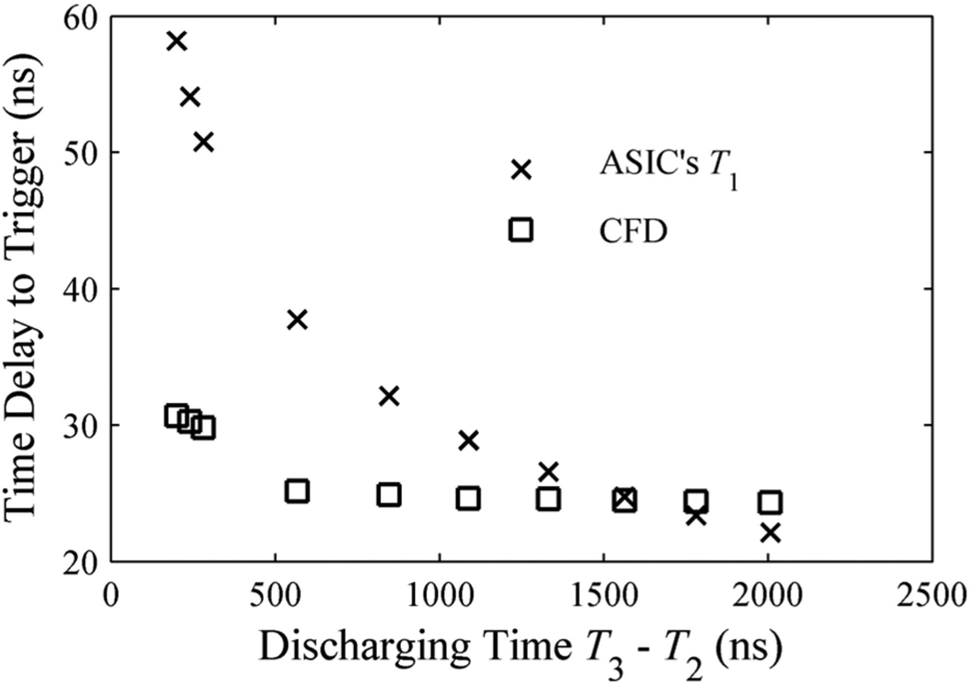
Time-walk error measured from the ASIC and a conventional CFD module with different signal levels. The vertical axis is the time difference between the input pulse and the T1 picked off by LE, and the horizontal is the width of the TQ output, which is proportional to the charge.
The time jitter from the ASIC chip and a CFD module (Canberra 454) is shown in Fig. 11. The ASIC’s timing performance is similar to that of the CFD module for signals at or above 400 pC. The best timing resolution of 111 ps (rms) was achieved for high-level signals. Even for signals at around the 100 pC charge level, the ASIC can still provide ns timing jitter, indicating that it is suitable for a non-time-of-flight PET coincidence event measurement.
Fig. 11.
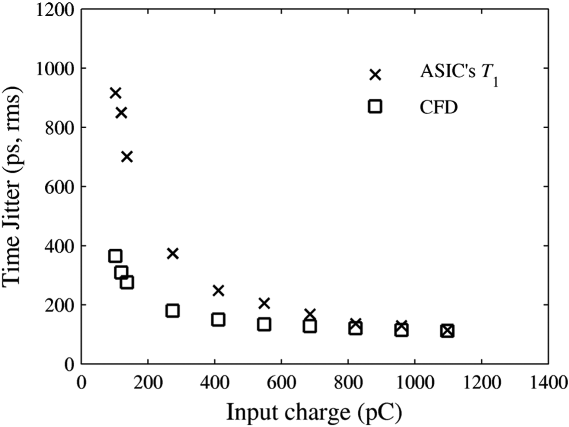
Time jitters measured for the ASIC and a conventional CFD module. The ASIC shows similar timing performance to that of the CFD at a high signal charge level, even with a much simpler circuit.
F. Measurements With LYSO/SSPM Detectors
The ASIC chip was tested with a PET detector that used an SSPM optically coupled to a LYSO scintillator. The energy spectrum measured from a 1.9 × 1.9 × 30 mm3 LYSO crystal and a22 Na source is shown in Fig. 12. The measured energy resolution of the 511-keV peak is 16.9% (FWHM), which is suitable for PET imaging applications.
Fig. 12.
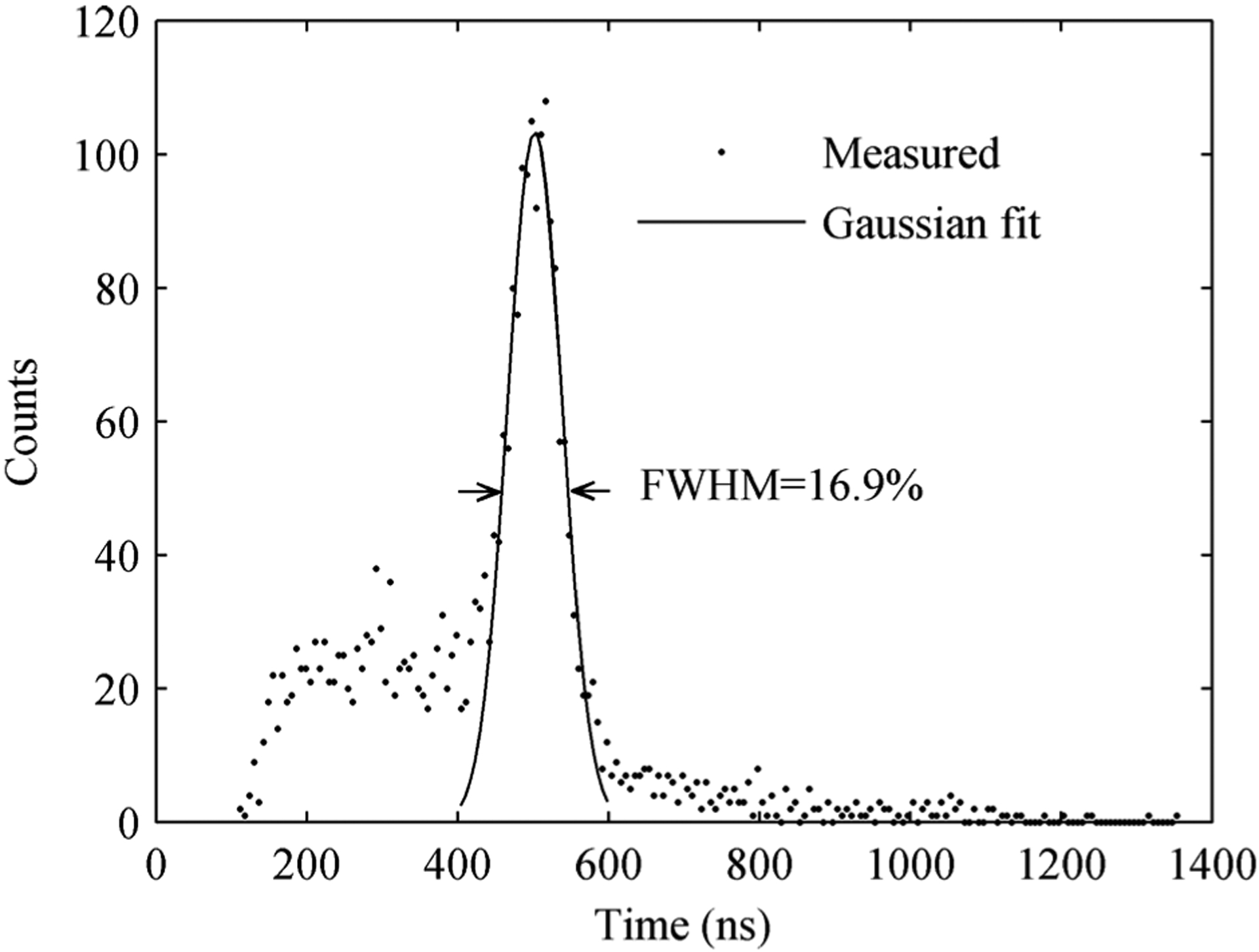
Energy spectrum of Na-22 measured with a 1.9 × 1.9 × 30 mm3 LYSO crystal coupled to an SSPM detector. The energy resolution of the 511-keV peak is 16.9% FWHM. The estimated measurement uncertainty was ~5%.
The coincidence timing resolution was measured using a 2 × 2 × 20 mm3 LYSO crystal with rough surfaces and was coupled to one SSPM at each end (dual-scintillator-ended readout) and a 1 × 1 × 10 mm3 LYSO crystal coupled to a fast PMT (Hamamatsu R7400), as shown in Fig. 13. Both SSPMs and PMTs were read out by two separate channels of the ASIC. The TT and TQ outputs of these two channels were sent to the LeCroy TDC 2228 module, T1, T2 and T3, and were digitized simultaneously. The discharging time (T3 – T2) was used for both the time-walk error correction and energy threshold.
Fig. 13.
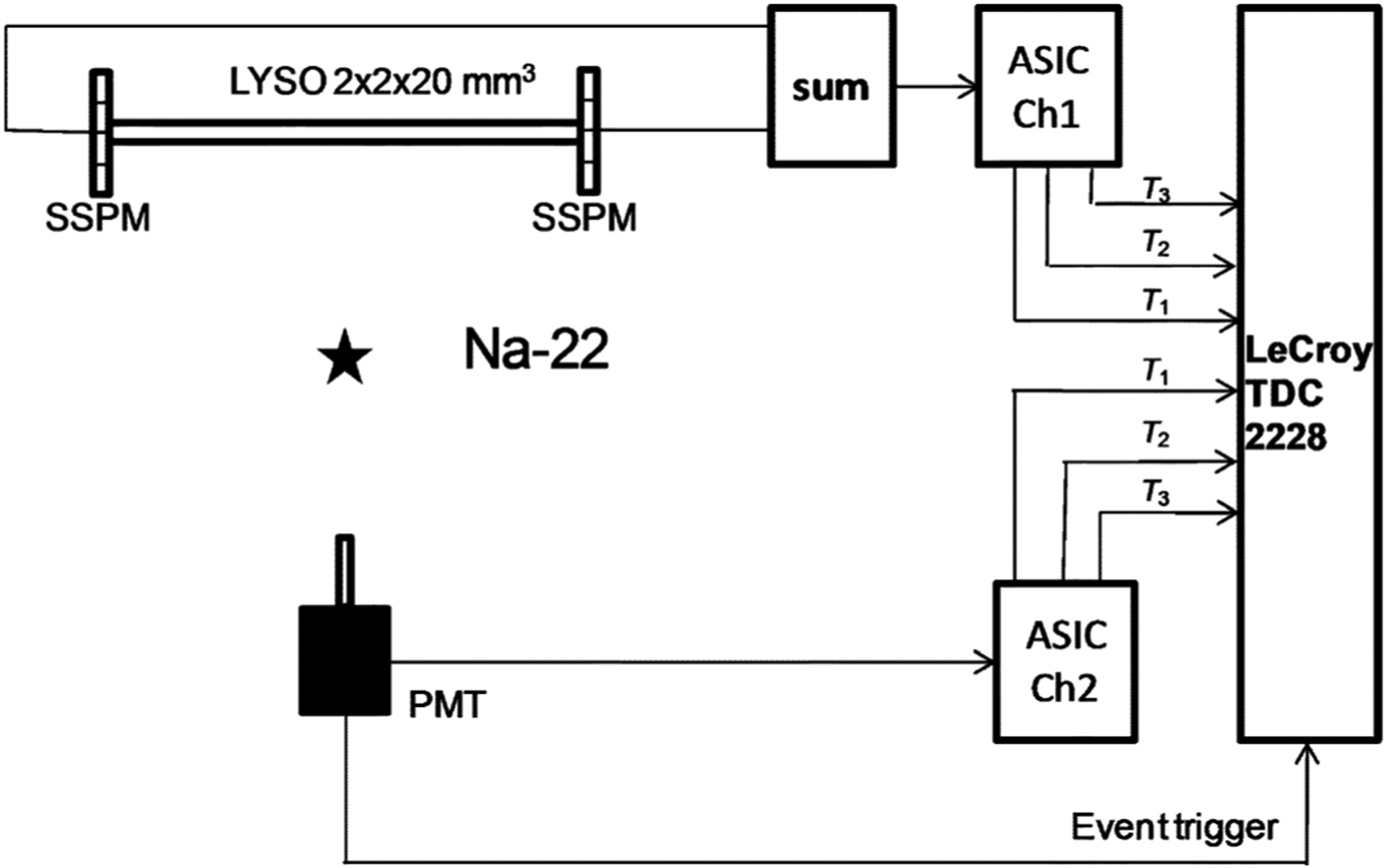
The test setup for coincidence timing measurement. One 2 × 2 × 20 mm3 LYSO crystal was read out by two SSPM arrays at both sides, and their signals were summed up and read out by one ASIC channel. Another 1 × 1 × 10 mm3 LYSO crystal was coupled to a fast PMT and read out by another ASIC channel.
The measured coincidence time spectrum is shown in Fig. 14. The timing resolution, after applying the time-walk error correction and energy window, is about 1.63 ns (FWHM). The time-walk error was corrected by a power function on the basis of the pre-calibrated data. The lower energy threshold was set to 420 keV. The dark count of the SSPM had a significant effect on the timing resolution.
Fig. 14.
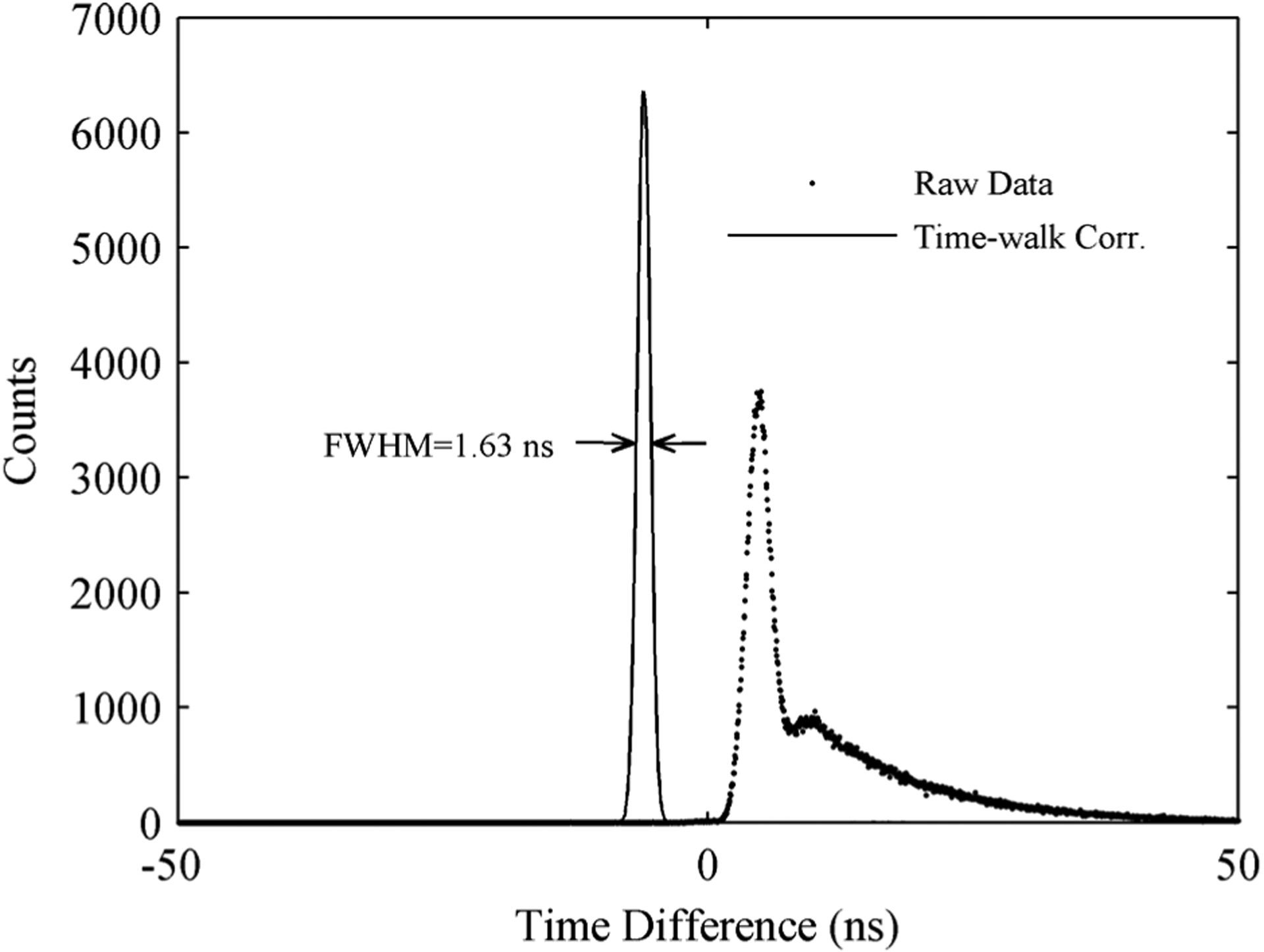
Measured coincidence time spectrum. The timing resolution is about 1.63 ns (FWHM) with the energy threshold set at 420 keV. The estimated measurement uncertainty was ~0.3 ns.
V. Conclusion
A time-based 8-channel ASIC has been developed and evaluated as front-end readout electronics for PET and other radiation detector applications. In contrast to a conventional ADC- and CFD-based approach, the new ASIC directly converts input signals into digital timing pulses that carry both the signal charge and timing information and can be processed by FPGA-based TDC only. In the design, a new charge-to-timing method was used to minimize circuit design complexity, power consumption, and intrinsic circuit noise. Our preliminary evaluation studies have shown that excellent linearity and accuracy in signal charge measurement have been achieved; around 200 ps or better timing resolution is reached for a detected signal energy around 511 keV, which is adequate for most non-TOF PET applications; the power consumption is less than 5 mW/ch under nominal operating conditions. Initial PET detector measurements of energy and coincidence timing resolutions with the ASIC have been conducted with similar results to those acquired with conventional ADC- and CFD-based electronics.
On the basis of these initial results, we conclude that the time based ASIC has achieved good performance by using the new QTC method, which fits well with the latest PET detectors that use compact SSPM arrays and require high-density and high-performance signal readout and processing electronics.
Acknowledgment
The authors would like to thank Prof. E.V. Hungerford at the University of Houston for supporting equipment during the chip tests. The authors would also like to thank ICC (Shanghai Integrated Circuit Research Center) for providing the MPW and other technique services.
This work was supported in part by R21EB007581 from the National Institute of Biomedical Imaging and Bioengineering, an IRG from The University of Texas MD Anderson Cancer Center, and by the National Nature Science Foundation of China under Grant 10975089.
Contributor Information
Zhi Deng, Tsinghua University, Beijing 100084, China..
Allan K. Lan, The University of Texas MD Anderson Cancer Center, Houston, TX 77030 USA..
Xishan Sun, The University of Texas MD Anderson Cancer Center, Houston, TX 77030 USA..
Chad Bircher, The University of Texas MD Anderson Cancer Center, Houston, TX 77030 USA..
Yinong Liu, Tsinghua University, Beijing 100084, China..
Yiping Shao, The University of Texas MD Anderson Cancer Center, Houston, TX 77030 USA..
References
- [1].Moehrs S et al. , “A detector head design for small-animal PET with silicon photomultipliers (SiPM),” Phys. Med. Biol, vol. 51, pp. 1113–1127, 2006. [DOI] [PubMed] [Google Scholar]
- [2].McElroy DP et al. , “Evaluation of silicon photomultipliers: A promising new detector for MR compatible PET,” Nucl. Instrum. Methods Phys. Res. A, vol. 571, pp. 106–109, 2007. [Google Scholar]
- [3].Schaart DR et al. , “A novel, SiPM-array-based, monolithic schintillator detector for PET,” Phys. Med. Biol, vol. 54, pp. 3501–3512, 2009. [DOI] [PubMed] [Google Scholar]
- [4].Shao Y, Li H, and Gao K, “Initial experimental studies of using solid-state photomultiplier for PET applications,” Nucl. Instrum. Methods Phys. Res. A, vol. 580, pp. 944–950, 2007. [Google Scholar]
- [5].Shao Y et al. , “Simultaneous PET and MR imaging,” Phys. Med. Biol, no. 10, p. 1965, 1997. [DOI] [PubMed] [Google Scholar]
- [6].Catana C et al. , “Simultaneous acquisition of multislice PET and MR images: Initial results with a MR-compatible PET scanner,” J. Nucl. Med, vol. 47, no. 12, pp. 1968–1976, 2006. [PubMed] [Google Scholar]
- [7].Pratte JF et al. , “Front-end electronics for the RatCAP mobile animal PET scanner,” IEEE Trans. Nucl. Sci, vol. 51, no. 4, pp. 1318–1323, August 2004. [Google Scholar]
- [8].Herrero-Bosch V et al. , “PESIC: An integrated front-end for PET applications,” IEEE Trans. Nucl. Sci, vol. 55, no. 1, pp. 27–33, February 2008. [Google Scholar]
- [9].Corsi F et al. , “ASIC development for SiPM readout,” in J. Instrum, 2009, p. P03004. [Google Scholar]
- [10].Koizumi M et al. , “Development of a low-noise analog front-end ASIC for APD-PET detectors,” Nucl. Instrum. Methods Phys. Res. A, vol. 604, pp. 327–330, 2009. [Google Scholar]
- [11].Callier S, “Silicon photomultiplier integrated readout chip (SPIROC) for the ILC: Measurements and possible further development,” in Proc. IEEE Nuclear Science Symp. Conf. Rec, 2009, pp. 42–46. [Google Scholar]
- [12].Wu J and Shi Z, “The 10-ps wave union TDC: Improving FPGA TDC resolution beyond its cell delay,” in Proc. IEEE Nuclear Science Symp. Conf. Rec, 2008, pp. 3440–3446. [Google Scholar]
- [13].Junnarkar S et al. , “FPGA based self calibrating 40 picosecond resolution, wide range time to digital converter,” in Proc. IEEE Nuclear Science Symp. Conf. Rec, 2008, pp. 3434–3439. [Google Scholar]
- [14].Jarron P et al. , “Time base readout of a silicon photomultiplier (SiPM) for time of flight positron emission tomography (TOF-PET),” in Proc. IEEE Nuclear Science Symp. Conf. Rec, 2009, pp. 1212–1219. [Google Scholar]
- [15].Fujiwara T and Takahashi H, “A new multi-level time over threshold method for energy resolving multi-channel systems,” in Proc. IEEE Nuclear Science Symp. Conf. Rec, 2008, pp. 3413–3415. [Google Scholar]
- [16].Shi B et al. , “Application of time-over-threshold readout method to micro strip gas chamber,” in Proc. IEEE Nuclear Science Symp. Conf. Rec, 2009, pp. 419–421. [Google Scholar]
- [17].Olcott PD and Levin CS, “Pulse width modulation: A novel readout scheme for high energy photon detection,” in Proc. IEEE Nuclear Science Symp. Conf. Rec, 2008, pp. 4530–4535. [Google Scholar]
- [18].Liu S et al. , “BES III time-of-flight readout system,” IEEE Trans. Nucl. Sci, vol. 57, no. 2, pp. 419–427, April 2010. [Google Scholar]
- [19].Sun X et al. , “Energy and timing measurement with time-based detector readout for PET applications: Principle and validation with discrete circuit components,” Nucl. Instrum. Methods Phys. Res. A, vol. 641, pp. 128–135, 2011. [DOI] [PMC free article] [PubMed] [Google Scholar]
- [20]. [Online]. Available: http://sensl.com/products/silicon-photomulti-pliers/spmarray4.