Abstract
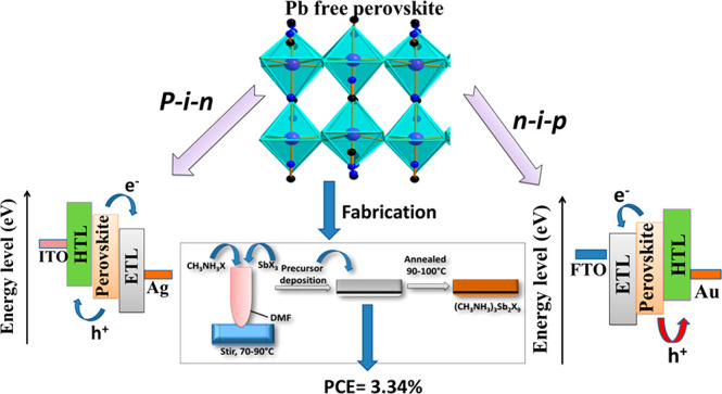
The recent trends and current state of perovskite solar cells (PSCs) suggested their potential for practical applications. Since their origin, organic–inorganic lead halide (MAPbX3) perovskite material-based PSCs have been widely attractive to the scientific community due to their simple manufacturing process, high performance, and cost effectiveness. In spite of the high performance, the lead halide perovskite solar cells are still agonizing due to the long-term stability and toxic nature of Pb. In the last 4 years or so, many alternative perovskite or perovskite-like materials were explored for the development of Pb-free PSCs. However, antimony (Sb)-based perovskite-like materials have shown enhanced stability and average photovoltaic performance. In this mini-review, we discuss the fabrication, recent trends, and current state of the Sb-based PSCs.
1. Introduction
The crystal structure of calcium titanate (CaTiO3) was discovered in 1839 and named perovskite.1 Perovskite is any material which satisfies the molecular formula of ABX3 (A = Cs+, CH3NH3+, NH2CHNH2+; B = Pb2+, Sn2+, Ge2+; and X = halide anion) and has crystal structure similar to that of CaTiO3. Several decades ago, a new perovskite structure CsPbX3 was designed and synthesized by the reaction between lead halide and cesium iodide.1 These perovskite structures have excellent optical and electrical properties which can be utilized in photovoltaic applications to produce the electrical energy on the consumption of sunlight.2 The most important feature of these perovskite materials is their high absorption coefficient.3 Although perovskite materials were prepared decades ago, they have been utilized as light absorbers in 2009 for photovoltaic applications.3 Further, numerous strategies and approaches were used for the development of highly efficient perovskite solar cells (PSCs). Basically, Pb-based perovskite materials like CsPbI3 and CH3NH3PbI3 (MAPbI3) have been widely explored in PSCs applications. Recently, the maximum power conversion efficiency (PCE) of >23% has been certified by NREL for Pb-based PSC.4 It was believed that PSCs can be applied in practical applications, but their poor long-term stability and the toxic nature of Pb limits their potential for outdoor applications. Hence, a quest toward the development of Pb-free PSCs led researchers to venture for an alternate Pb-free perovskite material. Antimony (Sb) is a less toxic element which has the potential to replace the Pb from the perovskite structures for the construction of PSCs.5 Jakubas et al.6 investigated the structural properties of the (CH3NH3)3Sb2I9 = MA3Sb2I9 in 1991, whereas Bagautdinov et al.7 studied the phase transition properties of the Cs3Sb2I9 perovskite-like structure in 1999. Although these Sb-based perovskite-like materials were introduced in the early 1990’s, their optoelectronic properties have been explored in the past few years. In this mini review, recent advances in the development of Sb-based PSCs have been summarized.
2. Construction of PSCs
Different device architectures of PSCs have been reported so far which also plays a crucial role in controlling the performance of the PSCs. In general, PSCs consist of five different components, which are (i) conductive transparent glass substrate, (ii) electron transport layer, (iii) light absorber, (iv) hole transport layer, and (v) metal contact. The fabrications of some PSC device architectures associated with Sb are discussed in this section (see Supporting Information for details).
2.1. Synthesis of Thin Films of A3B2X9 Perovskite-Like Materials
The quality of the prepared perovskite thin films influences the open circuit voltage and other photovoltaic parameters of the constructed PSCs. In this section, we summarize various synthetic approaches utilized to develop the high-quality perovskite films for PSCs.
2.2. One-Step Method
A one-step approach is the most widely used method to prepare the perovskite thin films for PSCs applications. In this approach, methylammonium halide and metal halide have been dissolved in solvent (such as N,N-dimethylformamide (DMF) or dimethyl sulfoxide (DMSO) with overnight stirring at 70–90 °C to complete the reaction. Further, this precursor solution is spin-coated onto the patterned FTO substrate and annealed at 90–100 °C for 20–30 min (Scheme S1a).
2.3. Two-Step Deposition Method
The perovskite films prepared in one step suffer from poor surface morphological features and rapid crystallization. Thus, a two-step method was introduced to prepare the perovskite thin films with improved morphological features. In this method, step (i) SbX3 in DMF is spin-coated onto the FTO glass substrate and annealed at 80–90 °C for 20–30 min. Further, antisolvents such as chlorobenzene or toluene are added to control the crystallization process, and in step (ii), CH3NH3X in 2-propanol is spin-coated and annealed at 80–90 °C for 20–30 min which resulted in the formation of high-quality thin films of (CH3NH3)3Sb2X9 (Scheme S1b).
2.4. Sequential Deposition Method
This method has been used to improve the quality of the perovskite films. In this approach, SbX3 in DMF is deposited onto the FTO glass substrate using the spin-coating method and annealed at 80–90 °C for 20–30 min. Further, this electrode is dipped in a solution of CH3NH3X in 2-propanol for 30–60 min and further annealed at 80–90 °C for 20–30 min. This yielded high-quality thin films of (CH3NH3)3Sb2X9 (Scheme S1c).
3. Structural and Optoelectronic Properties of A3B2X9 Perovskites
A3B2X9 (A = Cs+, Rb+, K+, CH3NH3+, NH4+; B = Sb3+; X = halide anion) perovskite-like materials possess excellent physiochemical and optoelectronic properties. A3B2X9 perovskite-like materials were synthesized a few decades ago, but their structural and optoelectronic properties have been investigated recently. In the last 3–5 years, due to excellent aerobic stability A3B2X9 perovskite-like materials have been employed as light absorbers for the construction of Pb-free PSCs.
3.1. Structural Properties of A3B2X9 Perovskite-Like Materials
In 1992, Jakubas et al.6 have synthesized and studied the phase transition properties of the MA3Sb2I9, whereas Cs3Sb2I9 was synthesized by Bagautdinov et al.7 using the Bridgman method in 1999. Yang et al.10 have found that the MA3Sb2I9 possesses hexagonal P63/mmc symmetry and crystal structure composed of antimony iodide octahedral layers with the voids between the layers filled with CH3NH3+. Further, Yang et al.10 also observed that in the case of replacing X = Br– instead of I–, (CH3NH3)3Sb2Br9 shown trigonal P3̅m1 symmetry. Zhang et al.11 synthesized (NH4)3Sb2I9 crystals using a novel synthetic approach, (NH4)3Sb2I9 crystallizes in a monoclinic crystal system with P21/n space group with a layered-type structure.11 In 2017, Zuo et al.12 also prepared (NH4)3Sb2I9 using antisolvent vapor-assisted crystallization. The crystal structure of (NH4)3Sb2I9, revealed central Sb atoms surrounded by six iodine atoms forming an octahedron, and nitrogen atoms were located at the tetrahedron center formed by four hydrogen atoms forming a 2D-layered structure. Furthermore, Buonassisi and co-workers have investigated the structural properties of all inorganic Cs3Sb2I9, Rb3Sb2I9, and K3Sb2I9 perovskite-like materials.13 The crystal structures of the Cs3Sb2I9 (0D), Rb3Sb2I9 (2D), and K3Sb2I9 (2D) were obtained using Rietveld refinement (Figure 1A–C). The Cs3Sb2I9 perovskite crystallizes in the P63/mmc (no. 194) space group where Sb2I93– dimers formed a 0D structure by sharing their triangular faces. In the case of K3Sb2I9 and Rb3Sb2I9, they crystallize in the P3̅m1 space group with cations Rb or Cs or K acting as spacers between the corner-sharing octahedral layers and formed 2D-network structures with Rb or K cations.13 This 2D structure formed when Rb or Cs or K acted as spacer between the corner-sharing octahedral layers and have space group of P3̅m1.13
Figure 1.
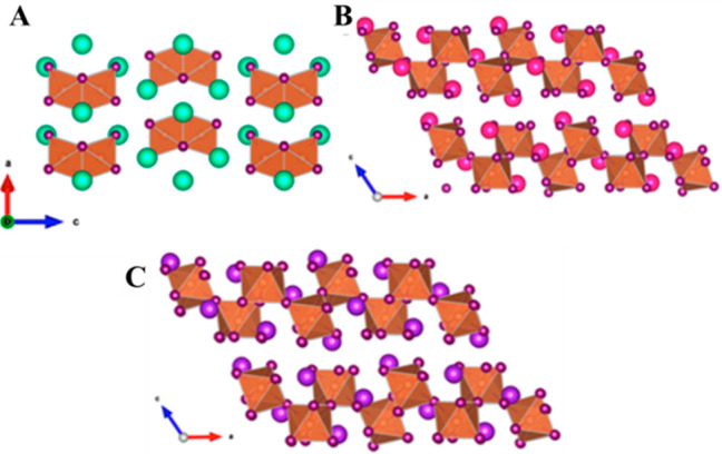
Crystal structures of Cs3Sb2I9 (A), Rb3Sb2I9 (B), and K3Sb2I9 (C) perovskite-like materials. Reprinted with permission from ref (13). Copyright 2018 American Chemical Society.
3.2. Optoelectronic Properties of A3B2X9 Perovskites
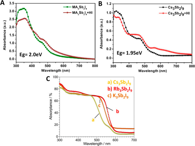
The optical band gap of the light-absorbing materials is very crucial for the construction of high performance PSCs. Zuo et al.12 have investigated the optical properties of the (NH4)3Sb2I9, which shows a band gap of 2.27 eV. In another work, Boopathi et al.14 reported that Cs3Sb2I9 has a band gap of 1.95 eV, whereas MA3Sb2I9 (where MA = CH3NH3+) has a band gap of 2.0 eV (Figure 2A,B). Buonassisi and co-workers investigated the optical properties of all inorganic Cs3Sb2I9, Rb3Sb2I9, and K3Sb2I9 perovskite-like materials using UV–vis absorption spectroscopy.13 The UV–vis spectra of the Cs3Sb2I9, Rb3Sb2I9, and K3Sb2I9 perovskite-like materials revealed a band gap of 2.43, 2.03, and 2.02 eV, respectively (Figure 2C).
Figure 2.
UV–vis spectra of MA3Sb2I9 (A) and Cs3Sb2I9 (B). Reprinted with permission from ref (13). Copyright 2018 American Chemical Society. UV–vis spectra of Cs3Sb2I9, Rb3Sb2I9, and K3Sb2I9 perovskite materials (C). Reprinted with permission from ref (14). Copyright 2017 Royal Society of Chemistry.
3.3. Progress in A3Sb2X9 Perovskite-Based PSCs
3.3.1. (NH4)3Sb2I9-Based PSC
PSCs were developed in 2009 by Miyasaka and co-workers with PCE of 3%, and this PCE was boosted to 20% within a few years.3,5 However, the poor stability of the Pb-based perovskite structure and the presence of Pb restricted their applications in large-scale production. Thus, numerous efforts have been made to develop highly stable PSCs with nontoxic or less toxic perovskite materials. Different metals such as Sn, Ge, Bi, Cu and Sb-based perovskite-like materials were employed for PSCs applications.5 Zuo et al.12 demonstrated the space charge limited current approach to determine the electron and hole mobility of the (NH4)3Sb2I9. Furthermore, Zuo et al.12 tuned the optical properties of the (NH4)3Sb2I9 by making a series of thin films of the perovskite materials (NH4)3Sb2I9, (NH4)3Sb2I6Br3, (NH4)3Sb2I3Br6, and (NH4)3Sb2Br9 which showed optical band gaps of 2.27, 2.49, 2.66, and 2.78 eV, respectively. Further, planar PSC devices were fabricated, and the PSC devices developed exhibited PCE ranging between 0.01% and 0.51%. These obtained PCEs were poor, but the developed PSCs device exhibited excellent open circuit voltage of 1003 mV for (NH4)3Sb2I9 based device.
3.3.2. MA3Sb2I9-Based PSCs
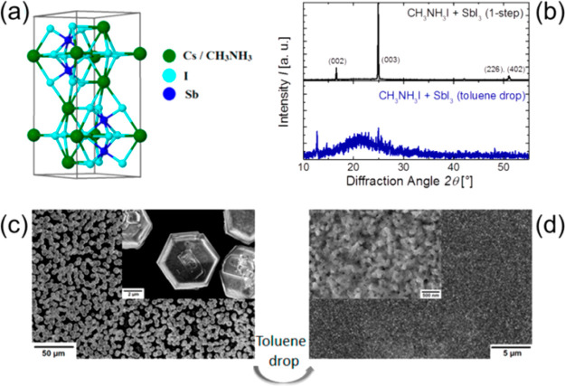
Hebig et al.8 developed the PSCs using MA3Sb2I9 as a visible light absorber. The MA3Sb2I9 thin films were prepared under nitrogen atmosphere using a solvent engineering method by employing toluene as an antisolvent to control the crystallization process. The MA3Sb2I9 crystallizes in the P63/mmc space group and the crystal structure is similar to that of MA3Bi2I9 and Cs3Sb2I9 (Figure 3a).8 The crystal structure of MA3Sb2I9 shows that (Sb2I9)3– is surrounded by three (CH3NH3)+ cations by hydrogen bonding interactions. The XRD patterns of the MA3Sb2I9 thin films prepared by one-step and two-step methods are shown in Figure 3b. The MA3Sb2I9 thin films prepared by one step showed a crystalline nature, whereas amorphous characters were present in the MA3Sb2I9 thin films prepared by a two-step method (Figure 3b). This amorphous nature may be due to toluene. The hexagonal surface morphology (Figure 3c) was observed for MA3Sb2I9 thin films prepared by a one-step method, whereas a nonhexagonal homogeneous and pinhole-free surface was obtained for MA3Sb2I9 thin films prepared by a two-step method (Figure 3d) by employing SEM.
Figure 3.
(a) Crystal structure of MA3Sb2I9, (b) XRD patterns of the MA3Sb2I9 thin films, (c) SEM images of the MA3Sb2I9 thin films prepared by one-step, and (d) two-step method. Reprinted with permission from ref (8). Copyright 2016 American Chemical Society.
The optoelectronic properties of MA3Sb2I9 thin films were investigated, which showed higher absorption coefficient of α > 105 cm–1 with a band gap of 2.14 eV which makes it a potential candidate for tandem solar cell applications.
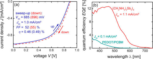
The planar PSCs were developed using MA3Sb2I9 light absorber, and photovoltaic performance was determined by short circuit photocurrent density–voltage (J–V) curves. The J–V curves of the fabricated PSCs (ITO/PEDOT:PSS(25 nm)/absorber/PC61BM(60 nm)/ZnO-NP(60 nm)/Al(150 nm) exhibited PCE of 0.49% with good open circuit voltage of 896 mV (Figure 4a). The external quantum efficiency (EQE) of the fabricated PSCs with device architectures (ITO/PEDOT:PSS (25 nm)/absorber/PC61BM(60 nm)/ZnO-NP (60 nm)/Al (150 nm) and ITO(120 nm)/PEDOT/PCBM/ZnO-NP/Al) were also investigated (Figure 4b). Boopathi et al.14 have obtained the high-quality thin films of MA3Sb2I9 by using additive such as hydroiodic acid (HI) to control the formation of MA3Sb2I9 thin films. The constructed PSCs with and without HI additive showed PCE of 2.04% and 1.11%, respectively. In another recent report, Giesbrecht et al.15 also reported the preparation of 2D layered MA3Sb2I9 for solar cell applications. The MA3Sb2I9 2D films were grown using antimony acetate precursor under glovebox. They have shown that 2D layered MA3Sb2I9 is a more efficient light absorber compared to the 0D MA3Sb2I9. The optoelectronic properties of the 0D and 2D layered MA3Sb2I9 were investigated. The direct and indirect band gap of the 2D layered MA3Sb2I9 was found to be 2.13 and 2.01 eV, respectively. In the case of 0D MA3Sb2I9, the absorption band was observed between 450 and 500 nm which suggested that 0D MA3Sb2I9 has a wide band gap. The PSCs was fabricated using SnO2 and TiO2 as compact and mesoporous layer, respectively. The highest PCE of 0.54% was achieved using TiO2 layer, whereas the lower PCE of 0.36% was reported for c-SnO2 based PSCs. The open circuit voltage of 570 mV was also reported for c-SnO2 based PSCs, which may be due to the better charge transport or lower recombination reactions. In 2020, Shaikh and co-workers have developed the PSCs using MA3Sb2I9 as light absorber5 by employing a two-step sequential deposition method to prepare the high-quality thin films of MA3Sb2I9. The sequential deposition method led to the formation of a uniform film of MA3Sb2I9 with a band gap of 2.1 eV. The highest occupied molecular orbital (HOMO) and lowest unoccupied molecular orbital (LUMO) energy level values of the MA3Sb2I9 were also determined by the combined study of cyclic voltammetry and UV–vis absorption spectroscopy. The constructed PSCs device with a two-step sequential deposition method showed the higher PCE of 0.54% with good open circuit voltage of 740 mV compared to the one-step approach (PCE = 0.1% and Voc = 690 mV). Authors have concluded that this improved PCE was attributed to the high-quality thin films (larger grain size, nonhexagonal surface morphology, and uniform surface coverage) and better charge extraction/electron transportation. It is believed that the morphological features of the absorber layer influence the photovoltaic parameters and performance of the PSCs.
Figure 4.
J–V curves (a) and EQE (b) of the PSCs (ITO/PEDOT:PSS (25 nm)/absorber/PC61BM (60 nm)/ZnO-NP (60 nm)/Al (150 nm). Reference device: ITO (120 nm)/PEDOT/PCBM/ZnO-NP/Al (green). Reprinted with permission from ref (8). Copyright 2016 American Chemical Society.
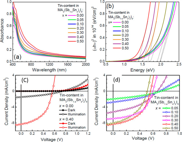
It is noteworthy to understand that the band gap of the absorber layer plays a crucial role and MA3Sb2I9 falls in the band gap range of 1.95–2.2 eV. The band gap of the perovskite materials can be easily tuned by doping with transition metals.16 Thus, Pal and co-workers inserted the Sn(IV) to the MA3Sb2I9 to obtain the low band gap light absorbers for photovoltaic applications.16 Here, authors have successfully employed Sn(IV) as a dopant due to its stability and less toxic nature. Different Sn(IV) contents (0%, 0.05%, 0.10%, 0.20%, 0.30%, 0.40%, and 0.50%) were explored to dope the MA3Sb2I9. The UV–vis spectra of the Sn(IV) doped MA3(Sb1–xSnx)2I (x = 0%, 0.05%, 0.10%, 0.20%, 0.30%, 0.40%, and 0.50%) were investigated to understand the impact of doping on the optical properties of MA3Sb2I9 (Figure 5a). The lowest band gap of 1.40 eV was found for MA3(Sb1–xSnx)2I with x = 0.50, whereas the higher band gap of 2.0 eV was reported for MA3(Sb1–xSnx)2I with x = 0 (Figure 5b). This showed that the increase of the Sn(IV) content reduced the band gap. Further, authors developed the p-i-n heterojunction PSCs with Cu@NiO and ZnO as hole and electron transporting layers, respectively. The highest PCE of 2.69% was achieved for the PSCs device developed using MA3(Sb1–xSnx)2I with x = 0.40 (Figure 5c). On the other hand, the lowest PCE of 0.57% was reported for MA3(Sb1–xSnx)2I with x = 0 based PSCs (Figure 5d). This suggested that the MA3Sb2I9 with narrow band gap and good morphological features may be a suitable candidate for photovoltaic applications.
Figure 5.
UV–vis spectra (a) and Tauc plot (b) of the MA3Sb2I9 doped with different Sn content. J–V curves of the PSCs based on MA3(Sb1–xSnx)2I with x = 0 and 0.40 (c) and x = 0.05, 0.10, 0.20, 0.30, 0.40, and 0.50 (d). Reprinted with permission from ref (16). Copyright 2018 American Chemical Society.
Nazeeruddin and co-workers also proposed a benign approach to control the dimensional growth and facilitate the heterogeneous nucleation by employing bis(trifluoromethane)sulfonimide lithium (LiTFSI). The introduction of LiTFSI led to the formation of 2D MA3Sb2I9–xClx films which showed the band gap of 2.05 eV. The highest PCE of 3.34% was reported with LiTFSI, while the lower PCE of 1.37% was achieved in the absence of LiTFSI.10 Authors also reported the excellent stability of the PSCs over 1400 h in ambient conditions.
3.3.3. Cs3Sb2I9-Based PSCs
All inorganic perovskite structures possess relatively higher stability compared to the organic–inorganic hybrid perovskite structures. Mitzi and co-workers reported the properties of the Cs3Sb2I9 and explored its potential for photovoltaic applications.17 The band gap of the Cs3Sb2I9 was found to be 2.05 eV. The PSCs with glass/FTO/c-TiO2/Cs3Sb2I9/PTAA/Au architecture exhibited open circuit voltage of 307 mV.17 Chu and co-workers also employed the Cs3Sb2I9 as a light absorber layer for Pb-free PSCs applications.14 They have constructed the PSCs with planar architecture and reported a PCE of 0.67%. Further, to improvise the morphological features, controlled surface, and to obtain uniform thin films, HI treatment was given to the Cs3Sb2I9 perovskite which led to enhanced PCE of 0.84%.
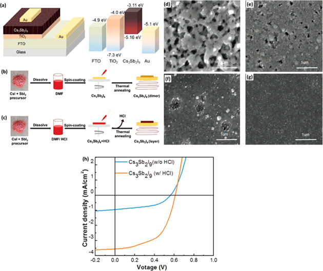
In general, the Cs3Sb2I9 exists in two different polymorphs, viz., 0D (dimer) and 2D (layered), where the dimer phase has a band gap of 2.50 eV, whereas layered Cs3Sb2I9 perovskite exhibits a band gap of 2.05 eV. The layered Cs3Sb2I9 also has an excellent absorption coefficient which makes it suitable for photovoltaic applications. Umar et al.18 developed the PSCs with mesoscopic structure using Cs3Sb2I9 light absorber layer. The dimer phase of Cs3Sb2I9 was obtained in the absence of HCl, whereas the layered structure of Cs3Sb2I9 was obtained in the presence of HCl. The Cs3Sb2I9 thin films were also prepared in the absence and presence of antisolvents (toluene, chlorobenzene, and isopropanol). The device structure and energy level diagram of the PSCs is shown in Figure 6a, and the synthesis route is shown in Figure 6b,c. According to the SEM results (Figure 6d–g), the grain size and improved crystallization was observed in the case of toluene (Figure 6e) and chlorobenzene (Figure 6f), but some voids were still present. The highly uniform and pinhole/void-free Cs3Sb2I9 thin films were obtained in the presence of isopropanol (Figure 6g). However, in the absence of antisolvents, poor crystallization of the Cs3Sb2I9 thin film was observed (Figure 6d). This suggested that the presence of isopropanol as antisolvent could avoid the short circuit and reduce the trap states. The improved PCE of 1.21% was achieved with HCl, whereas the lower PCE of 0.43% was observed in the absence of HCl additive (Figure 6h). Singh et al.19 also found better photovoltaic properties in the Cs3Sb2I3 material with layered polymorph phase (band gap of 2.05 eV) compared to the dimer polymorph (band gap of 2.3 eV) of Cs3Sb2I3. The constructed PSCs with inverted planar heterojunction architecture (ITO/PEDOT:PSS/Cs3Sb2I9/PC70BM/C60/BCP/Al) exhibited the best PCE of 1.5% using Cs3Sb2I3 perovskite with layered phase. However, relatively lower PCE of 0.83% was achieved for Cs3Sb2I3 with the dimer form. This may be due to the relatively lower band gap and better optoelectronic properties of the layered Cs3Sb2I3 structure. Further, to address the most important aspect of the device, the stability of these all-inorganic perovskite materials was also explored. The stability of the Cs3Sb2I3 polymorphs (dimer and layered) was studied by Chonamada et al.,20 and they found that the dimer form of the Cs3Sb2I3 degraded in 49 days whereas the layered form degraded in 88 days. Authors also found that water, heat, and light equally cause the degradation of Cs3Sb2I3. This showed that Cs3Sb2I3 can be employed as an efficient light absorber layer for Pb-free PSCs applications.
Figure 6.
Schematic diagram of PSCs device and energy level diagram (a). Schematic synthetic view of Cs3Sb2I9 without (b) and with (c) HCl. SEM images of the Cs3Sb2I9 thin films prepared without antisolvent (d) and with antisolvents of toluene (e), chlorobenzene (f), and isopropanol (g). J–V curves of the PSCs device (h). Reprinted with permission from ref (18). Copyright 2019 John Wiley and Sons.
3.3.4. Rb3Sb2I9-Based PSCs
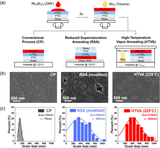
Johnston et al.21a investigated the properties of Rb3Sb2I9 nanoparticles as a newer class of perovskite material which has a direct and indirect band gap of 2.24 and 2.1 eV, respectively. Harikesh et al.22a reported photovoltaic properties of the Rb3Sb2I9 and found that Rb3Sb2I9 has P1c1 space group. Authors also found that Rb3Sb2I9 is thermally stable up to 250 °C. The PSCs device with mesoscopic structure exhibited the PCE of 0.66% with open circuit voltage of 550 mV. According to the theoretical investigations, it was proposed that Rb3Sb2I9 with layered structure can achieve the highest photocurrent density of ∼10 mA/cm2. The Rb3Sb2I9 has good stability and absorption coefficient, which makes it another suitable Pb-free light absorber material. Since the cationic group influences the exciton binding energy, structural dimensionality, optoelectronic and photovoltaic performance, Buonassisi and co-workers investigated the optical/photovoltaic properties of the various perovskite-like materials (K3Sb2I9, Cs3Sb2I9, and Rb3Sb2I9).13 The K3Sb2I9, Cs3Sb2I9, and Rb3Sb2I9 have band gap of 2.02, 2.43, and 2.03 eV, respectively, and revealed that K3Sb2I9 and Cs3Sb2I9 exhibited poor PCE whereas Rb3Sb2I9-based PSCs showed improved PCE of 0.76%. Weber et al.23a studied the effect of iodide to bromide ratio and tuned the band gap of the Rb3Sb2I9. The optical band gap was changed by tuning the halide composition (Rb3Sb2I9, Rb3Sb2Br9-xIx, and Rb3Sb2Br9) and the fabricated PSCs (n-i-p solar cell structure) showed the best PCE of 1.37% with excellent photocurrent density (4.25 mA/cm2) and exhibited the excellent stability up to 150 days for Rb3Sb2I9-based PSCs, and 85% of the initial PCE was retained. The perovskite light absorber with large grain size improves the carrier mobility, influencing the performance of the PSCs and lifetime. Thus, photovoltaic performance of the PSCs can be enhanced by extending the carrier drift/diffusion length. So far, the largest grain size of the Rb3Sb2I9 was found to be 200 nm. Therefore, it will be of great significance to prepare the Rb3Sb2I9 thin films with larger grain size for efficient photovoltaic devices. In this regard, Li et al.24a obtained the conventional process (CP), high-temperature vapor annealing (HTVA), and reduced supersaturation annealing (RSA) processed Rb3Sb2I9 perovskite thin films (Figure 7a). The HTVA processed Rb3Sb2I9 thin film showed the smooth film surface (Figure 7b), larger grains (600 nm), and void-free surface compared to the RSA-processed Rb3Sb2I9 thin film (Figure 7c).
Figure 7.
(a) Depiction of essential process step in CP, RSA, and HTVA. (b) SEM images of the resulting films and (c) corresponding grain size distributions. Reprinted with permission from ref (24a). Copyright 2020 Royal Society of Chemistry.
Accordingly, the best PCE of 1.35% was obtained for HTVA processed Rb3Sb2I9 thin film based PSCs, whereas the relatively lower PCE of 1.12% was achieved for RSA processed Rb3Sb2I9 thin film. The poor PCE of 0.38% was reported for the CP processed Rb3Sb2I9 thin film. The PCE of the HTVA processed Rb3Sb2I9 thin film based PSCs was due to the larger grain size, which improved the carrier mobility and lifetime.
3.3.5. Other Sb-Based Perovskite Like Materials
Adonin et al.9 investigated the optical and photovoltaic features of the N-ethylpyridinium bromoantimonate (V) = (N-EtPy)[SbBr6] and developed the inverted planar PSCs. The (N-EtPy)[SbBr6] materials has a band gap of 2.25 eV, which suggested its potential as energy material for tandem solar cells. Authors developed the inverted planar PSCs with different electron transport layers (6,6-phenyl C61 butyric acid methyl ester = PCBM and N,N′-bis(2-ethylhexyl)-perylenediimide = PDI). The PSCs with PCBM achieved the PCE of 2.8%, whereas the device fabricated with PDI as electron transport layer showed PCE of 3.2%.9 The photovoltaic performance of the inverted planar PSCs (ITO/PEDOT:PSS/1/PDI/Ag) were also compared with standard device architecture (ITO/TiOx/1/P3HT/Au). The standard device architecture of PSCs exhibited the improved PCE of 3.8%, which may be due to the better charge extraction and fast electron transport process. Moreover, the higher open circuit voltage of 1285 mV was achieved using standard device architecture.9 This work suggested that the photovoltaic performance of the PSCs may be further improved by reducing recombination reactions and improving charge extraction. Li et al.21b reported 0D tetranuclear perovskite-like material heteromorphic hybrids [(C7H18N2O)3Sb4I18·H2O and (C7H18N2O)Sb2I8·H2O (where C7H18N2O2+ = N-aminopropylmorpholinium)]. The (C7H18N2O)3Sb4I18·H2O and (C7H18N2O)Sb2I8·H2O exhibited the optical band gap of 1.71 and 2.11 eV, respectively. This kind of perovskite-like hybrid material has the potential for use in photovoltaic applications. Jia et al.22b reported Cu3SbI6 as a light absorber, which has indirect band gap of 2.43 eV. They constructed the PSCs with device structure of ITO/PEDOT:PSS/Cu3SbI6/PC61BM/Al, which showed the good open circuit voltage of 704 mV along with the PCE of 0.50%. Deng and co-workers proposed a new antimony–silver halide double perovskite light absorber ((CH3NH3)2AgSbI6) for photovoltaic applications.23b This perovskite, (CH3NH3)2AgSbI6, has a band gap of 1.93 eV and showed good stability up to 370 days. Vargas et al.24b also reported a direct band gap of copper–antimony halide perovskite material (Cs4CuSb2Cl12) and investigated its optoelectronic properties. The Cs4CuSb2Cl12 perovskite showed good stability and has a very narrow band gap of 1.02 eV, which suggested its potential application in the development of Pb free PSC. Nie et al.25b reported methylammonium antimony sulfur diiodide (MASbSI2) perovskite-like structure (band gap = 2.03 eV) as light absorber, and the PSCs device exhibited good PCE of 3.08%. The photovoltaic performance of the Sb-based PSCs have been summarized in Table 1.
Table 1. Photovoltaic Parameters of the Reported PSCs with Different Light Absorbers.
| sample | absorber layer | FF (%) | Voc (V) | Jsc (mA/cm2) | PCE (%) | ref |
|---|---|---|---|---|---|---|
| 1. | MA3Sb2I9-xClx | 65 | 0.70 | 7.38 | 3.34 | (10) |
| 2. | (NH4)3Sb2I9 | 42.5 | 1.03 | 1.15 | 0.51 | (12) |
| 3. | Rb3Sb2I9 | 63 | 0.66 | 1.84 | 0.76 | (13) |
| 4. | K3Sb2I9 | 50 | 0.338 | 0.41 | 0.07 | (13) |
| 5. | Cs3Sb2I9 | 58 | 0.404 | 0.13 | 0.03 | (13) |
| 6. | MA3Sb2I9+HI | 60 | 0.62 | 5.41 | 2.04 | (14) |
| 7. | Cs3Sb2I9+HI | 48 | 0.60 | 2.91 | 0.84 | (14) |
| 8. | MA3Sb2I9 | 52 | 0.46 | 2.21 | 0.54 | (15) |
| 9. | MA3Sb2I9 | 47 | 0.74 | 1.40 | 0.54 | (5) |
| 10. | Sn doped MA3Sb2I9 | 58 | 0.56 | 8.32 | 2.70 | (16) |
| 11. | Cs3Sb2I9 | 37 | 0.68 | 4.62 | 1.26 | (19) |
| 12. | Rb3Sb2I9 | 57 | 0.55 | 2.11 | 0.66 | (22) |
| 13. | Rb3Sb2I9 | 40 | 0.61 | 5.54 | 1.35 | (24) |
| 14. | Bromoantimonate (V) (N-EtPy)[SbBr6] | 58 | 1.2 | 5.1 | 2.50 | (9) |
| 16. | MASbSI2 | 58 | 0.65 | 8.12 | 3.08 | (25a) |
4. Conclusions and Future Perspectives
Antimony (Sb)-based perovskite materials are an emerging class of perovskite-like materials with good optoelectronic features. In the past few years, compared to the Pb-based perovskite materials, Sb-based perovskite-like materials have excellent stability and less toxic nature, which makes them alternative potential light absorbers for Pb-free PSCs applications. The band gap of the Sb-based perovskite-like materials lies in the range of 1.95–2.43 eV, attempts are made to reduce the band gap by insertion of less toxic metal to the Sb-based perovskite-like structures. So far, to the best of our knowledge, the best developed perovskite solar cells devices based on Sb-based perovskite-like structures exhibited the highest PCE of 3.34%, which is remarkably good performance compared to the other nontoxic perovskite materials. The research on Sb-based perovskite-like materials is still in the initial phase in terms of PCE and still needs to be further improved by employing novel approaches. The major challenges with Sb-based perovskite-like materials are wide band gap, poor morphological features, uncontrolled crystallization process, poor electron transportation, and water sensitivity. These challenges may be addressed by the following efforts: (i) the wide band gap should be narrowed by inserting less toxic and highly stable metals, (ii) the morphological features and crystallization process can be controlled by introducing new additives and antisolvents, (iii) the design and synthesis of new charge extraction layers/electron transport layers would be of great significance to improve the performance of the perovskite solar cells, and (iv) the water sensitivity of the Sb-based perovskite-like materials can be improved by introducing hydrophobic cations to the perovskite structures.
Acknowledgments
K.A. would like to thank UGC, New Delhi, India (Scheme No./RGNFD/2014-15) for research fellowship. S.M.M. would like to thank CSIR, New Delhi, India for financial support (File no. 01(2935)/18/EMR-II). Authors sincerely acknowledged Discipline of Chemistry, IIT Indore for research grant.
Biographies
Dr. Khursheed Ahmad has completed Ph.D. in the Discipline of Chemistry, Indian Institute of Technology Indore, India. After Ph.D., Dr. Khursheed Ahmad continued his research work with Dr. Shaikh M Mobin, Discipline of Chemistry IIT Indore. His current research interests include perovskite solar cells, especially lead-free perovskite solar cells, electrochemical sensors, and wastewater treatment (photocatalysis and adsorption).
Dr. Shaikh M. Mobin accomplished his Bachelor’s and Master’s degrees from Wilson College, University of Mumbai with major in Chemistry and Ph.D. from Mumbai University in Chemistry. In 2012, he joined IIT Indore and is now working as an Associate Professor in the Discipline of Chemistry. He had developed his multidisciplinary research group working in a wide area of research including solid-state structural transformation, design and synthesis of newer class of MOFs and their applications in energy storage, conversion and biomedical devices, exploring metal nano-oxide materials for energy storage, conversion, optical and electrochemical sensing, metal nano-oxide materials derived by employing metal complexes/MOFs as single-source molecular precursors as catalyst in organic transformation, and developing greener c-dots for bioimaging and biomarkers. Moreover, the research group designs and synthesizes small molecules as cellular organelles target and docking. Finally, our group at IIT Indore is also involved in the development of advanced and novel materials for all aspects of solar energy harvesting and perovskite-based lead-free solar cells including absorber material, electrode materials, hole-transport, and electron acceptor materials as well as blocking layer.
Supporting Information Available
The Supporting Information is available free of charge at https://pubs.acs.org/doi/10.1021/acsomega.0c04174.
Construction of PSCs (PDF)
The authors declare no competing financial interest.
Supplementary Material
References
- Kour R.; Arya S.; Verma S.; Gupta J.; Bandhoria P.; Bharti V.; Datt R.; Gupta V. Potential Substitutes for Replacement of Lead in Perovskite Solar Cells: A Review. Global Challenges 2019, 3, 1900050. 10.1002/gch2.201900050. [DOI] [PMC free article] [PubMed] [Google Scholar]
- a Ahmad K.; Mobin S. M. Graphene Oxide based Planar Heterojunction Perovskite Solar Cell under Ambient Condition. New J. Chem. 2017, 41, 14253–14258. 10.1039/C7NJ02847D. [DOI] [Google Scholar]; b Jiang F.; Yang D.; Jiang Y.; Liu T.; Zhao X.; Ming O. Y.; Luo B.; Qin; et al. Chlorine-Incorporation-Induced Formation of the Layered Phase for Antimony-Based Lead-Free Perovskite Solar Cells. J. Am. Chem. Soc. 2018, 140, 1019–1027. 10.1021/jacs.7b10739. [DOI] [PubMed] [Google Scholar]
- Kojima A.; Teshima K.; Shirai Y.; Miyasaka T. Organometal halide perovskites as visible-light sensitizers for photovoltaic cells. J. Am. Chem. Soc. 2009, 131, 6050–6051. 10.1021/ja809598r. [DOI] [PubMed] [Google Scholar]
- Kanda H.; Shibayam N.; Huckab A. J.; Lee Y.; Paek S.; Klipfel N.; Roldan-Carmona C.; Queloz V. E.; Grancini G.; Zhang; et al. Band-bending Induced Passivation: High Performance and Stable Perovskite Solar Cells using a Perhydropoly(silazane) Precursor. Energy Environ. Sci. 2020, 13, 1222–1230. 10.1039/C9EE02028D. [DOI] [Google Scholar]
- Ahmad K.; Kumar P.; Mobin S. M. A Two-Step Modified Sequential Deposition Method-based Pb-Free (CH3NH3)3Sb2I9 Perovskite with Improved Open Circuit Voltage and Performance. ChemElectroChem 2020, 7, 946–950. 10.1002/celc.201902107. [DOI] [Google Scholar]
- Jakubas R.; Decressain R.; Lefebvre J. NMR and Dilatometric Studies of the Structure Phase transitions of (CH3NH3)3Sb2I9, and (CH3NH3)3Bi2I9 Crystal. J. Phys. Chem. Solids 1992, 53, 755–759. 10.1016/0022-3697(92)90185-G. [DOI] [Google Scholar]
- Bagautdinov B.; Novikova M. S.; Aleksandrova I. P.; Blomberg M. K.; Chapuis G. X-ray study of phase transitions in Cs3Sb2I9 crystal. Solid State Commun. 1999, 111, 361–366. 10.1016/S0038-1098(99)00217-3. [DOI] [Google Scholar]
- Hebig J. C.; Kühn I.; Flohre J.; Kirchartz T. Optoelectronic Properties of (CH3NH3)3Sb2I9Thin Films for Photovoltaic Applications. ACS Energy Lett. 2016, 1, 309–314. 10.1021/acsenergylett.6b00170. [DOI] [Google Scholar]
- Adonin S. A.; Frolova L. A.; Sokolov M. N.; Shilov G. V.; Korchagin; et al. Antimony (V) Complex Halides: Lead-Free Perovskite-Like Materials for Hybrid Solar Cells. Adv. Energy Mater. 2018, 8, 1701140. 10.1002/aenm.201701140. [DOI] [Google Scholar]
- Yang Y.; Liu C.; Cai M.; Liao Y.; Ding Y.; Ma S.; Liu X.; Guli M.; Dai S.; Nazeeruddin M. K. Dimension-controlled Growth of Antimony-based Perovskite-like Halide for Lead-free and Semitransparent Photovoltaics. ACS Appl. Mater. Interfaces 2020, 12, 17062–17069. 10.1021/acsami.0c00681. [DOI] [PubMed] [Google Scholar]
- Zhang H.; Fang L.; Yuan R.-Z. Triammonium nonaiododiantimonate(III), (NH4)3[Sb2I9]. Acta Crystallogr., Sect. E: Struct. Rep. Online 2005, 61, i70–i72. 10.1107/S1600536805011098. [DOI] [Google Scholar]
- Zuo C.; Ding L. Lead-free Perovskite Materials (NH4)3Sb2IxBr9_x. Angew. Chem., Int. Ed. 2017, 56, 6528–6532. 10.1002/anie.201702265. [DOI] [PubMed] [Google Scholar]
- Correa-Baena J. P.; Nienhaus L.; Kurchin R. C.; Shin S. S.; Wieghold S.; Hartono; et al. A-Site Cation in Inorganic A3Sb2I9 Perovskite Influences Structural Dimensionality, Exciton Binding Energy, and Solar Cell Performance. Chem. Mater. 2018, 30, 3734–3742. 10.1021/acs.chemmater.8b00676. [DOI] [Google Scholar]
- Boopathi K. M.; Karuppuswamy P.; Singh A.; Hanmandlu C.; Lin L.; Abbas S. A.; Chang C. C.; Wang P. C.; Li G.; Chu C. W. Solution-Processable Antimony-based Light-absorbing Materials Beyond Lead Halide Perovskites. J. Mater. Chem. A 2017, 5, 20843–20850. 10.1039/C7TA06679A. [DOI] [Google Scholar]
- Giesbrecht N.; Weis A.; Bein T. Formation of stable 2D Methylammonium Antimony Iodide Phase for Lead-free Perovskite-like Solar Cells. J. Phys.: Energy 2020, 2, 024007. 10.1088/2515-7655/ab78ef. [DOI] [Google Scholar]
- Chatterjee S.; Pal A. J. Tin(IV) Substitution in (CH3NH3)3Sb2I9: Towards Low Band Gap Defect-Ordered Hybrid Perovskite Solar Cells. ACS Appl. Mater. Interfaces 2018, 10, 35194–35205. 10.1021/acsami.8b12018. [DOI] [PubMed] [Google Scholar]
- Saparov B.; Hong F.; Sun J. P.; Duan H.-S.; Meng W.; Cameron S.; Hill I. G.; Yan Y.; Mitzi D. B. Thin-Film Preparation and Characterization of Cs3Sb2I9: A Lead-Free Layered Perovskite Semiconductor. Chem. Mater. 2015, 27, 5622–5632. 10.1021/acs.chemmater.5b01989. [DOI] [Google Scholar]
- Umar F.; Zhang J.; Jin Z.; Muhammad I.; Yang X.; Deng H.; Jahangeer K.; Hu Q.; Song H.; Tang J. Dimensionality Controlling of Cs3Sb2I9 for Efficient All-Inorganic Planar Thin Film Solar Cells by HCl-Assisted Solution Method. Adv. Opt. Mater. 2019, 7, 1801368. 10.1002/adom.201801368. [DOI] [Google Scholar]
- Singh A.; Boopathi K. M.; Mohapatra A.; Chen Y. F.; Li G.; Chu C. W. Photovoltaic Performance of Vapor-Assisted Solution-Processed Layer Polymorph of Cs3Sb2I9. ACS Appl. Mater. Interfaces 2018, 10, 2566–2573. 10.1021/acsami.7b16349. [DOI] [PubMed] [Google Scholar]
- Chonamada T. D.; Dey A. B.; Santra P. K. Degradation Studies of Cs3Sb2I9: A Lead-Free Perovskite. ACS Appl. Energy Mater. 2020, 3, 47–55. 10.1021/acsaem.9b01899. [DOI] [Google Scholar]
- a Johnston A.; Dinic F.; Todorovic P.; Chen B.; Sagar L. K.; Saidaminov M. I.; Hoogland S.; Voznyy O.; Sargent E. H. Narrow Emission from Rb3Sb2I9 Nanoparticles. Adv. Opt. Mater. 2020, 8, 1901606. 10.1002/adom.201901606. [DOI] [Google Scholar]; b Li Y.; Xu Z.; Liu X.; Tao; et al. Two Heteromorphic Crystals of Antimony-Based Hybrids Showing Tunable Optical Band Gaps and Distinct Photoelectric Responses. Inorg. Chem. 2019, 58, 6544–6549. 10.1021/acs.inorgchem.9b00718. [DOI] [PubMed] [Google Scholar]
- a Harikesh P. C.; Mulmudi H. K.; Ghosh B.; Goh T. W.; Teng Y. T.; Thirumal K.; Lockrey M.; Weber K.; Koh T. M.; Li S.; Mhaisalkar S.; Mathews N. Rb as an Alternative Cation for Templating Inorganic Lead-Free Perovskites for Solution Processed Photovoltaics. Chem. Mater. 2016, 28, 7496–7504. 10.1021/acs.chemmater.6b03310. [DOI] [Google Scholar]; b Jia X.; Ding L. A Low-temperature Solution-processed Copper Antimony Iodide Rudorffite for Solar Cells. Sci. China Mater. 2019, 62, 54–58. 10.1007/s40843-018-9300-6. [DOI] [Google Scholar]
- a Weber S.; Rath T.; Fellner K.; Fischer R.; Resel R.; Kunert; et al. Influence of the Iodide to Bromide Ratio on Crystallographic and Optoelectronic Properties of Rubidium Antimony Halide Perovskites. ACS Appl. Energy Mater. 2019, 2, 539–547. 10.1021/acsaem.8b01572. [DOI] [Google Scholar]; b Li Y.-J.; Wu T.; Sun L.; Yang; et al. Lead-free and Stable Antimony–Silver-Halide Double Perovskite (CH3NH3)2AgSbI6. RSC Adv. 2017, 7, 35175–35180. 10.1039/C7RA06130G. [DOI] [Google Scholar]
- a Li F.; Wang Y.; Xia K.; Hoye R. L. Z.; Pecunia V. Microstructural and Photoconversion Efficiency Enhancement of Compact Films of Lead-Free Perovskite Derivative Rb3Sb2I9. J. Mater. Chem. A 2020, 8, 4396–4406. 10.1039/C9TA13352F. [DOI] [Google Scholar]; b Vargas B.; Ramos E.; Perez-Gutierrez E.; Alonso J. C.; Solis-Ibarra D. A Direct Bandgap Copper–Antimony Halide Perovskite. J. Am. Chem. Soc. 2017, 139, 9116–9119. 10.1021/jacs.7b04119. [DOI] [PubMed] [Google Scholar]
- a Nie R.; Mehta A.; Park B.-W.; Kwon H.-W.; Im J.; Seok S. I. Mixed sulfur and iodide-based lead-free perovskite solar cells. J. Am. Chem. Soc. 2018, 140, 872–875. 10.1021/jacs.7b11332. [DOI] [PubMed] [Google Scholar]; b Nie R.; Mehta A.; Park B.-W.; Kwon H.-W.; Im J.; Seok S. I. Mixed sulfur and iodide-based lead-free perovskite solar cells. J. Am. Chem. Soc. 2018, 140, 872–875. 10.1021/jacs.7b11332. [DOI] [PubMed] [Google Scholar]
Associated Data
This section collects any data citations, data availability statements, or supplementary materials included in this article.


