

Abstract
Research in bioelectronics is highly interdisciplinary, with many new developments being based on techniques from across the physical and life sciences. Advances in our understanding of the fundamental chemistry underlying the materials used in bioelectronic applications have been a crucial component of many recent discoveries. In this Review, we highlight ways in which a chemistry-oriented perspective may facilitate novel and deep insights into both the fundamental scientific understanding and the design of materials, which can in turn tune the functionality and biocompatibility of bioelectronic devices. We provide an in-depth examination of several developments in the field, organized by the chemical properties of the materials. We conclude by surveying how some of the latest major topics of chemical research may be further integrated with bioelectronics.
Keywords: Bioelectronics, Biointerfaces, Biophysical chemistry, Electrochemistry, Photoelectrochemistry, Synthetic chemistry, Surface chemistry
1. Introduction
Blurring the boundaries between biotic and abiotic systems, bioelectronics is catalyzing profound progress in diagnoses, therapy, prosthetics, as well as facilitating a deeper understanding of physiological processes. New directions and activities are emerging in the bioelectronics community, which signify that this is an active, exciting field with numerous unexplored questions. Some of the recent developments include advanced materials synthesis,1, 2 closed-loop neural3, 4 and cardiac5–8 interfaces, 3D seamless integration of chronic bio-interfaces,9–12 in vivo real-time biosensing,11–16 therapeutics for restoring lost neural functions and reversing neurodegenerative disorders,17–21 etc.
Generally, the validation and optimization of material and bioelectronics devices are heavily focused on engineering and functional considerations. Electrical circuits of various scales and geometries have been designed and manufactured to interrogate bioelectrical phenomena with high fidelity and sensitivity over a wide range of spatial scales.22 At the small end, there is the nanoscale subcellular level, where relevant devices include single-channel patch-clamp and nanoscale field effect transistors. Individual cells and colonies exist on the micron to millimetre scale, where electrical monitoring is typically performed with whole-cell patch-clamp or extracellular electrodes. At the mesoscale tissue-level, microelectrode arrays and mesh electrodes are the most widely used tools for monitoring. To obtain tissue monitoring with fine spatial resolution, the integration of hundreds of electrodes in parallel arrays have been developed for simultaneous signal collection. Furthermore, more functionalities, such as drug delivery, optogenetics, MRI or acoustic imaging, and wireless signal transductions, have been factored and assembled into integrated probes intended for more sophisticated investigations of biological activities using integrated fabrication and engineering techniques.23–26
While the engineering aspects of bioelectronics are extensively discussed elsewhere,27–32 the coverage of chemistry-specific developments in the literature has been comparatively sparse. Despite this, they have aided in creating a new functional material toolkit, in tailoring traditional materials to achieve long-lasting functioning, and in improving probe efficacy and functionality. In this review (Fig. 1), fundamental synthetic chemistry, surface chemistry, electrochemistry, and biophysical chemistry in bioelectronics are discussed first. Next, we summarize new chemical advances that are essential for bioelectronics performance under each category of material (i.e., inorganic or organic semiconductors or conductors, Table 1). These processes play fundamental and indispensable roles to advance the field as they produce new material components, optimize cost-efficient production, promote biocompatibility and long-term stability, improve electrochemical and biophysical performance, and help reveal new biophysical mechanisms and functionalities at biointerfaces. At the end of the review, we discuss new chemistry opportunities for future bioelectronics.
Figure 1.
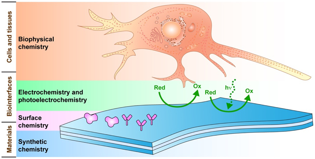
Chemistry aspects of bioelectronics.
Table 1.
Summary of advantages, disadvantages and example applications of the material groups used for fabrication of bioelectronics devices.
| Advantages | Disadvantages | Application Examples | |
|---|---|---|---|
| Inorganic semiconductors | - Established industrial processing - Colloidal structures can be synthesized - Mostly crystalline material - Available surface modification methods - Tunable electrical and optical properties |
- Larger material rigidity - Mechanical mismatch at the biointerfaces - Some materials are highly cytotoxic |
- Resorbable devices134, 157, 160 - Intracellular stimulation38, 67, 129 - Intracellular recording43, 175 - Membrane voltage sensor225 |
| Organic semiconductors | - Solution processable - Flexible and can be intrinsically stretchable - Available surface and bulk modification methods - Tunable electrical and optical properties - Generally low cytotoxicity |
- Lower carrier mobility - Stability in air and in vivo may be poor - May have low crystallinity |
- Stretchable sensors273 - Bioelectronic sensing291, 294 - Optical modulation308, 317 |
| Inorganic conductors | - Established fabrication methods - Good stability - Colloidal structures can be synthesized - Mostly crystalline material - Available surface modification methods - Excellent and stable electrical conductivity - Generally low cytotoxicity |
- Larger material rigidity - Mechanical mismatch at the biointerfaces |
- Recording microelectrodes336, 342, 352, 353, 358, 362 - Intracellular electrochemical detection405, 407 - Wearable electronics404, 427 - In vivo monitoring16 |
| Organic conductors | - Solution processable - Suitable for additive manufacturing (e.g., inkjet printing, 3D printing) - Flexible and can be intrinsically stretchable - Can have high water content - Available surface and bulk modification methods - Tunable electrical conductivity - Generally low cytotoxicity |
- Low chemical stability - May need to manage the conductive phases within the material - May have low crystallinity |
- Stretchable electronics465 - In vivo recording469 - Transparent electronics478 - Chemical assembly in living cells494 |
2. Fundamentals at biointerfaces
In this section, we want to accustom the reader to the fundamentals of working with junctions between the various materials and biological structures, which are referred to as biointerfaces. First, we discuss the size and time scale of the formation of interfaces and how they affect our choice of materials. We follow with a discussion on the basic biophysical principles behind the transduction of biological signals. Finally, we describe the concepts of mechanical matching between natural and artificial systems and the importance of their biochemical stability.
2.1. Size scales of bioelectronics
Biointerfaces can be formed at different length scales depending on the relevant biological question and application, ranging from large-area non-specific modulation to subcellular sensing (Fig. 2a). The following discussion provides not only a description of biointerface design but also a historical perspective on the field of bioelectronics. Relatively large, noninvasive electrodes were developed first and remain widely used today. For recording, those applications are mainly electroencephalography (EEG) for recording brain activity through the scalp, electrocardiography (ECG) for recoding of cardiac activity, and electromyography (EMG) for investigation of skeletal muscles. Similarly, large-area stimulations are routinely used in emergency cardiac arrest defibrillation, in physical therapy for electrical muscle stimulations, and to effectively treat some mental illnesses through electroconvulsive therapy.33 By definition, large-area techniques have limited resolution and suboptimal efficiency due to making indirect contact and being placed far from the tissue of interest. The bioelectrical effects are averaged over a large area and it is therefore difficult to disentangle the variety of chemical interactions at this scale.
Figure 2.
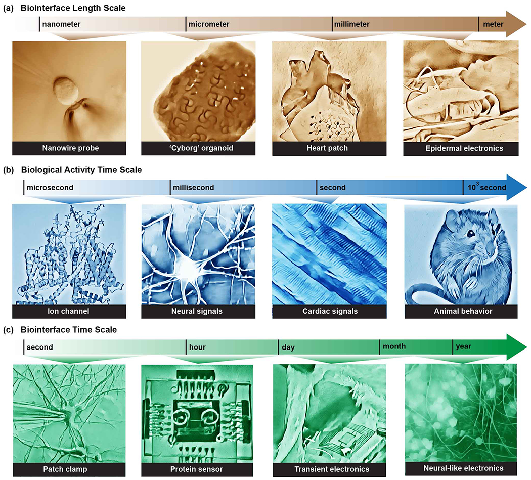
Bioelectronics and bioelectrical studies span a range of length and time scales. Awareness of chemistry and physics at all applicable levels is necessary to devise appropriate synthetic and analytical methods for the study of biointerfaces.
Progress in materials research brought the possibility of the creation of probes with higher resolution placed closer to the active cells, which facilitated the development of smaller and less invasive devices. The first step was the development of direct biointerfaces with a single organ. These efforts brought us artificial pacemakers, cochlear implants, and deep-brain stimulation probes, which improved survival and quality of life for millions of people. However, the realization of challenging goals such as visual prosthetics or brain-machine communication requires single-cell resolution. Traditional electronics face certain key limitations in such applications. Namely, they possess undesirable mechanical properties, limited biocompatibility, and low interface resolution.
The advent of modern micro- and nanotechnology opened the next frontier in bioelectronics2, 11, 12, 23, 29, 32, 34–40. Probes became smaller and more adaptable, improving the biocompatibility of devices. Micron-sized devices allowed for measurement of local electric potentials deep inside tissues and interfacing with small groups of cells, bringing a whole new insight into the study of cell physiology. On this scale, substantial chemical interactions between the materials and the tissues, such as adhesive forces, have to be taken into account. Current state-of-the-art devices are capable of forming exact single-cell extracellular41 and intracellular42, 43 interfaces. Hopefully, further development in the field will produce methods for single organelle modulation or even studies on specific cell structures such as microfilaments or ion channels. Such measurements will become highly local and allow the study of heterogeneity44 and non-equilibrium processes in living cells. On the lowest scale, chemical and mechanical energy terms become approximately equal in magnitude,45 which will without doubt reveal the presence of new fundamental processes.
With increased spatial resolution comes decreased signal throughput through the biointerface. While large-area recordings give only average readings of electrical activity, such recordings are generally more useful for practical applications. Signals from single cells are usually not representative of the entire tissue and can carry significant noise. Therefore, another challenge that comes with utilizing microscale biointerfaces is achieving high parallelization of modulation and recording. For this purpose, massive amounts of bioelectronic components have to be fabricated or assembled. Recently, significant effort has been put into clinical translation of machine-brain interface technologies by Neuralink. Recent reports demonstrate simultaneous recording from 1020 electrodes.46 While this number is ten-fold higher than those of classic microelectrode arrays (e.g., Utah or Michigan probes),47–52 it is still far from that achieved by biological interfaces. For example, human auditory nerves are made of some 30,000 myelinated neuron fibers53 and optical nerves of more than a million.54 The number of neuronal connections necessary to establish a high-fidelity computer-brain interface is still a matter of debate. However, with the first devices entering clinical trials,55, 56 we should expect a better quantitative assessment of these technologies over the next few decades. It can be envisioned that new materials in a form of massively self-assembled neuro-mimetic fibrils will one day match the parallelization of information transfer observed in nature. A recent report showing bundles of microwires used for neuronal recording represents a promising early step in this direction.57 It is therefore important to study nanoscale self-assembly processes, dynamic combinatorial libraries and other types of parallel chemistries for the synthesis of future bioelectronic devices.
2.2. Time scales of bioelectronics
The relevant time scales in the bioelectronics can be seen from two orthogonal perspectives. One describes the time scale over which biological signals are generated (Fig 2b), and the other is the duration of the biointerface, that is, the time that the device and the biological system spend in contact. (Fig 2c). The timing of recording and stimulation with respect to the biological events will be discussed first. For interfacing with highly active cells such as neurons or cardiac muscles, which can fire an action potential on the timescale of milliseconds, a high frequency response is required from the device. For investigations of even more transient biological events such as the action of molecular motors or activity of single ion channels, even higher temporal resolution on the timescale of nano- to microseconds is required. The timing of the target process therefore determines the required kinetics of the recording or stimulation. For example, for studies of transient states, using diffusion-limited processes would be unwise. Conversely, devices meant to sense or stimulate slower physiological processes such as bone regeneration58 require less temporal resolution but carry with them a different set of considerations. In this case, interfacial chemistry plays an important role as interactions such as adhesion have a significant effect on the stability of an interface as well as any immune response it can elicit. Likewise, devices that can potentially impact mechanotransduction or chemical transduction must consider the time scale of these processes, where signals are delivered and processed with significant delay, on the order of minutes to hours. Understanding the required stimulation or response frequency is thus a critical factor in matching the design of devices with their specific applications.
The other independent time scale is the period over which we expect our biointerface to be active. The interfacing time scale can range from extremely transient experiments to permanent implantation for clinical applications. Biointerfaces used in studies of individual physiological processes can be relatively short-lived. They are used to study single physiological interactions and disposed of soon after. As such, these types of experiments do not require extensive studies of stability and biocompatibility. Maintaining stable biointerfaces becomes a concern for experiments with tissues or cell cultures. In this case, devices need to maintain their integrity and it becomes important to evaluate additional interactions in the biointerface beyond the designated purpose of the device. If for example, the products of the device decomposition lead to uncontrolled proliferation of cells or increased cytotoxicity, such interactions cannot be ignored. It is therefore critical to take into account the chemical composition of such devices as well as the reactivity of their constituents. For applications requiring implantations of the device into an organism, not only does device stability have to be higher, but additional considerations have to account for the immune system response to the presence of a foreign body. The origin and methods of mitigation of immune response to the biointerface will be discussed in the following section. Excellent stability and biocompatibility are required for a long-term integration of bioelectronics with a host body. An important example of an application that requires long-term integration is the formation of chronic brain interfaces. The delicate nature of brain tissue makes it not only more sensitive to invasive probes, but due to the brain’s limited regeneration ability, replacement of used bioelectronics devices with new ones is not a feasible solution. Each removal and insertion of probes causes irreversible trauma that can lead to fatal accumulation of damages. Therefore, clinical applications of the machine-brain interface demand stable, long-term biointerfaces.
For long-term integration of bioelectronics, additional attention has to be paid to all the secondary electronics necessary for their operation. Bench-top controllers, transducers, and power sources can be used in short-term laboratory experiments without concern. The case is significantly different for implantable bioelectronics, where electrodes tethered to extensive external instrumentation limits the mobility of host organisms and makes such a solution impractical. Hence, lightweight and, ideally, remote-controlled recording and modulation devices represent an important design principle that requires significant thought. The essential issue is the integration of bioelectronic devices with proper microscale power supplies. Recent developments point to devices to which power can be delivered remotely, e.g., through magnetic resonant coupling.59 Another front is led by the freestanding devices that lack traditional electric circuits, but can locally stimulate tissues through magnetothermal,23, 60 chemomagnetic,61 photoelectrochemical,62, 63 photothermal,64–67 and photoacoustic38, 68 effects that are initiated with remotely delivered physical stimuli. Future research in applied bioelectronics will no doubt veer towards the development of integrated, wireless devices for the ultimate goal of seamless, inconvenience-free bionic integration.
2.3. Signal transductions
Biological systems fundamentally differ from standard electronics by their mechanisms of signal generation and transmission. In conventional conductors such as metals, the majority of electric charge is carried directly by electrons. In biological systems, rich in water, ions, and organic matter, electric current is carried mostly by ionic fluxes. These two modes of conduction are, in principle, very dissimilar, which requires a specific interface in which signals can be transduced (Fig. 3).
Figure 3.
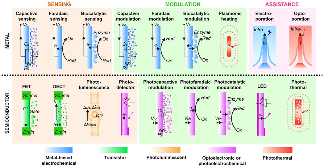
Signal transduction mechanisms in bioelectrical interfaces can vary depending on the material design and chemistry. Top: Metal-based electrodes can be used for recording or injection of capacitive, faradaic, and biocatalytic currents. Free-standing metallic nanostructures allow used for plasmonic heating. Additionally, metallic structures can be used to facilitate interface interrogation penetrating cellular membranes using electroporation and optoporation. Bottom: Highly sensitive recording of bioelectric signals using field-effect transistor (FET) and organic electrochemical transistors (OECT). Readout of optical signals using photoluminescent materials and photodetectors. Free-standing nanoscale semiconductors allow for wireless injection of currents through photocapacitive, photofaradaic and photocatalytic effects. Micro light-emitting diodes (LED) can be used to deliver optical signals. Semiconductors without electric and radiative energy decay pathways can generate photothermal heating.
2.3.1. Bioelectricity in cells and tissues
Electrically active cells communicate via spikes of ion fluxes caused by a sudden release of ions, known better as action potentials. The potential difference between insides of cells and their extracellular environment (usually negative) is maintained by active transport and imbalance in the concentration of ions, typically K+ and Na+. The resting transmembrane potential existing due to this imbalance is classically described using the Goldman-Hodgkin-Katz (GHK) equation:
| Equation (1) |
where Vrest is the resting membrane potential, R is the ideal gas constant, T is the absolute temperature, and F is the Faraday constant. The sums account for permeabilities P and concentrations [M] of monovalent ions on the inside and outside of the membrane.69 The resting membrane potential is the mechanism by which cells store energy used for signaling. When stimulation occurs, passive ion channels open and ions freely flow in and out of the membrane. This ion flux generates electric currents which can create a local potential change in the tissue, effectively meaning this cell is interacting with neighboring cells to cause further signal transduction. A potential generated at point (x,y,z) by moving ions can be derived from Ohm’s law and, treating the ions as pure monopoles, takes the form of:
| Equation (2) |
where Ii is the current from the ith monopole, σ is the conductivity of the medium, and ri is the distance from the monopole to the point (x,y,z).69
The aforementioned model averages molecular interactions and approximates properties of the media and the surrounding tissues. In reality, the environment of biological fluids is highly crowded, and in dense structures, e.g., brain tissue, electrodiffusion is affected by heterogeneities at a molecular level.70 Hence deviations from this classic interpretation can be observed on a subcellular length scale. Such heterogeneities can arise from the extracellular environment and interactions with large proteins and charged species, as well as from uneven spatial distribution of ion channels in the membrane. Therefore, it is paramount that the progress in nanodevices’ research comes together with the development and validation of new theoretical models.70
2.3.2. Electrochemical sensing or modulation processes
The most straightforward electrode-tissue interface utilizes capacitive currents (Fig. 3). A chemically inert electrode can only inject current due to building capacitive charge on its surface due to applied potential. Ions with complementary charges will migrate towards the electrode, creating charge currents, and start building up a layer on the electrode surface called an electrical double layer (EDL). Ionic currents will flow only until the electrode is fully charged. The time constant for EDL formation can be described as:
| Equation (3) |
where Re and Ce are the leakage resistance and capacitance of the electrode, respectively. This simple relation is an essential operational specification of the electrode. It describes its operational limits as well as its bandwidth – the maximum frequency at which signals can be delivered or received. The electrical interaction between the electrode and the membrane can be estimated with a highly simplified model of an equivalent circuit, in which the cell and electrode are treated as potential sources, an interface is modelled as a parallel capacitor and a resistor, and an additional term is added for internal electrode resistance.71 Using this equivalent circuit and Equation 2, we can derive the relation between cell and electrode potentials:
| Equation (4) |
where Ve is the electrode potential, Vcell is the potential at the cell surface, Rint is electrode’s internal resistance, and s is the complex frequency of interacting waveforms. The above equation can be used to qualitatively describe both stimulation and recording. For stimulation, we choose to control electrode potential Ve and interact with the cell. For recording, the cell is firing its active potential Vcell, and we measure readings received on the electrode.
By analyzing Equation 4, fundamental qualities of electrode-cell biointerfaces can be derived. First, electrical interaction, as parameterized by the potential, is inversely proportional to the distance r between the electrode and cell membrane. Hence the closer the distance between the electrode and the membrane, the stronger the interaction. Also, for strong interactions, it is recommended to keep leakage resistance (Re) low and electrode capacitance (Ce) high. Resistance of interconnections plays a role in determining the signal-to-noise ratio (SNR) of the biointerface. For higher currents, Rint has to be kept low, but for good SNR, it has to be kept high. For designs in which the electrode is bifunctional and used for recording and stimulation, a compromise has to be made.
Purely capacitive electrodes rely only on EDL and have a limited range of operation. Stimulation with higher potentials can be accomplished using electrodes injecting Faradaic currents (Fig. 3). Such an electrode is chemically active and introduces new ions due to electrochemical reduction or oxidation occurring on its surface. It has been shown that highly catalytic electrodes are capable of stimulating with strong potentials.72 The drawback of using a chemically active electrode is its degradation over time. One possible way to prevent extensive damage to an electrode injecting Faradaic current is the application of principles used for the fabrication of supercapacitors.73 These principles include the application of nearly completely reversible electrochemical reactions or precise structuring of the electrode on the atomic level, which permit increasing its capacity beyond the limit of traditional materials. Another possible development in this field might be the application of bioelectrocatalysis (Fig. 3), which uses electrode-bound enzymes to generate active species in situ for selective stimulation or process metabolites present in the system to be used for their detection.74, 75 Additionally, although redox signaling is paramount in biological systems,76, 77 it was not thoroughly explored with respect to bioelectronic modulation.
2.3.3. Optoelectronic or photoelectrochemical sensing or modulation processes
Semiconductor-based optoelectronics or photoelectrochemical devices can be used to deliver (e.g., using a light emitting diode [LED] or a photovoltaic device) or read out (e.g., using an in vivo photometer) stimulation signals at the biointerface, when matched with electrical circuits or wireless microcontrollers (Fig. 3).78, 79 To perform single cell studies, we can either use semiconductor structures/devices that are microns or nanometres in size, or use highly localized initial stimuli (e.g., a laser spot) over macroscopic structures/devices.
Many of the devices for such studies are based on diode junctions. In particular, for photoelectrochemical stimulation applications, a photovoltaic mechanism is often adopted.62 A diode device is typically created when hole-rich (p-type) and electron-rich (n-type) semiconductors are placed in contact, causing a shift in their valence and conduction bands near the p-n junction, within a region called the depletion zone. Photoexcitation can promote an electron from the valence to the conduction band, creating an electron-hole pair.38 The electrons and holes then diffuse away from the depletion zone in accordance with their charge, creating a potential difference on different parts of the device that can be used to stimulate cells and tissues similarly to wired electrodes described above.
Depending on the material, photoexcitation can inject capacitive current, Faradaic current, or a combination thereof into the biointerface (Fig. 3). These processes in freestanding structures can be understood within a framework analogous to that of the wired electrode. However, semiconductors are highly sensitive to their environment through the alteration of their surfaces’ electronic structure. Photostimulation and other physical behaviors at the interfaces can be predicted both qualitatively and quantitatively using the concept of band bending. Band bending in semiconductor describes the alteration in native electronic structure due to the material environment, surface modification,80 or the material size and dimensionality.81 Semiconductor physics and electronic processes underlaying their photoactivity require a more thorough discussion, for which we redirect readers to literature specific to semiconductors.32, 38
2.3.4. Photothermal modulation processes
The photothermal effect arises from radiationless energy transfers in photoexcited materials. That is, the emitted energy translates into the kinetic energy of the material or its surroundings, and the temperature increases. In practice, this means that the best candidates for photothermal modulation primary respond to excitation with the generation of phonons or plasmons. In crystalline materials, nonradiative recombination can produce quantized oscillations in the bulk material, known as phonons, which are responsible for photothermal heating in those structures.82 For certain metallic nanomaterials, such as noble metal nanoparticles and carbon nanostructures, light absorption results in oscillations of associated free electrons on the material surface. These oscillations are referred to as surface plasmons, and their production can convert almost all incoming light energy to heat.83, 84 Continuous-wave irradiation of plasmonic materials can therefore create strong temperature gradients (Fig. 3).64
Transduction of thermal signals is another vital aspect of biophysics, yet it has not been studied as extensively as electrical signals. Cell physiology, especially the catabolic process responsible for energy generation, generates multiple intracellular and extracellular thermal gradients.85 Such signals can trigger proliferation and affect other cellular metabolic pathways. It can be deduced from the GHK equation (Eq. 1) that temperature affects membrane potential, and its increase will make it more sensitive to stimulations. Additionally, multiple ion channels have been discovered to be especially receptive to temperature gradients such as thermosensitive potassium channel TREK-1.64 For thermal sensing, purely resistive microelectromechanical devices as well as a range of nanostructures have proven effective. Quantum dots, upconverting nanoparticles, and metal cluster were all applied to create remote luminescent thermometers.86
A closely related phenomenon can be observed when instead of steady irradiation, high-power pulsed lasers are used to illuminate plasmonic nanostructures. A sudden release of energy causes evaporation of solvents around the material surface, forming gas nanocavities which, upon collapsing, release ultrasonic waves traveling through the medium. This phenomenon is referred to in the literature as a photoacoustic effect.65, 68, 87 Although the mechanism of the generation of photoacoustic waves is not fully understood it allowed the development of a variety of imaging and stimulation methods.88, 89 Recently, the photoacoustic effect was used to facilitate entry of recording electrodes into the cells through the local optoporation mechanism in a similar manner to the classical electroporation (Fig. 3), but providing superior process control and cell viability.90 However, potential applications of the photoacoustic effect in bioelectronics remain largely unexplored.
2.3.5. Transistor-based sensing processes
Transistors are some of the most important elements in nearly all modern electronics and bioelectronics. In particular, field-effect transistors (FETs, Fig. 3) are widely used as they have been extensively studied due to their importance in the operation of integrated circuits. In the regular planar configuration, a semiconductor substrate is connected to a source (S), drain (D), and gate (G) electrodes. The gate electrode is separated from the substrate using a dielectric insulator. When a voltage potential is applied between the source and drain electrodes, the current will flow through the semiconductor channel. The current through the semiconductor will be proportional to the potential applied to the gate. Depending on the doping of the semiconductor substrate, a transistor can operate in enhancement or depletion mode. For an ideal transistor in enhancement mode, no current flow will occur at gate potential below the specific threshold and beyond the threshold potential, current will rise linearly until saturation current is reached. The behavior is reversed in a depletion mode transistor. The ratio of current change to the applied potential in a transistor is defined as transconductance gm and can be a direct measure of its sensitivity.
The external connection to the gate is typically omitted for bioelectronic sensing applications, as the gate potential variation is generated directly by the dynamic processes from charged species or cells. Notably, for FET-based detection of binding of unbinding of charged species (such as protein marker), the sensitivity is limited to the characteristic Debye screening length:
| Equation (5) |
Where lb is the Bjerrum length, Σi is the sum of present ion species with concentrations ρi and valence zi. The Debye screening length can be used to approximate sensitivity range and is on the order of <1 nm in concentrated electrolytes.38 Specificity and sensitivity of FETs in bioelectronic situations can be improved by using surface modifications with biomolecules capable of molecular recognition.91 The advantage of FET devices over metal-based capacitive and faradaic electrodes is that device current flows in a closed-circuit, so that the potential issues with the electrode impedance, electrode corrosion or biological invasiveness can be minimized. This also allows FET devices to achieve faster response times92 and lower SNR93 when compared to single terminal electrodes.
The second type of transistor – electrolyte gated transistor – has gained increased popularity in bioelectronics over the recent years due to its high transconductance, biocompatibility, and processing versatility. In this configuration, the semiconducting substrate and gate are replaced with porous structures which can be interpenetrated by ions increasing or decreasing current flow through the channel. The most popular materials for gating channels are made of organic conductors and semiconductors forming a class of organic electrochemical transistors (OECTs, Fig. 3). Transconductance in OECTs can be described using Bernards model94, 95 and the equation:
| Equation (6) |
which accounts for channel geometry: width W, length L, and thickness d; charge carrier mobility μ; capacitance per unit volume of a channel C*; gate voltage VG and specific threshold voltage Vth. Capacitance in organic materials can be widely tuned; therefore, characteristic of OECTs is their exceptionally high transconductance.96 OECTs can be used for ion-selective sensing with the introduction of proper membranes.97 A closely related topic to OECTs is a class of hydrogel-based devices called organic electronic ion pumps (OEIPs) which can be used for ion delivery98–100 and as drug delivery platforms.3, 95, 101 For a detailed discussion on OECTs and OEIPs we direct the readers to recent reviews focusing on these subjects.102, 103
2.3.6. Stimulation with molecular and optical signals
Biological systems utilize a range of small molecules and peptides for intracellular or organism-wide signaling. Bioelectronic devices can be used to deliver signaling molecules and pharmaceuticals directly into tissue, increasing their availability and potency.104 Microfluidic channels present one promising approach to this application. The drawback of this approach is that it requires the integration of secondary elements, such as pressure sources, to function properly. Although some micropumps with low power consumption have been devised,105, 106 there is still much progress to be made in this area. An alternative approach is to design materials that can dispense drugs from inside their structure on-demand such as the aforementioned OEIPs. However, volumetric materials have limited cargo capacity, and molecules are usually delivered through diffusion and positive pressure, which lowers delivery speed and efficiency.
Apart from some small organisms, most cells and tissues cannot be directly stimulated using light. Two approaches exist to make ordinary cells susceptible to optical signals: optogenetics and optopharmacology. Optogenetics relies on genetic modification of target cells to display specially engineered optically responsive ion channels,107 while optopharmacology relies on delivery of photoresponsive drugs which, while inactive in their native form, can be distributed evenly among cells and will become active only upon illumination.108 Both of these approaches, which are discussed further in section 7.2.2, allow for local optical modulation of cellular activity. Delivery of light to the stimulation location can be accomplished using waveguides or microlight sources such as upconverting materials, or micro-LEDs.109 Efficiency of light delivery can be calculated using the equation:
| Equation (7) |
where Ps is the output power of the source, η factors are coupling and scattering efficiency, and Φ is the geometric factor of the light interface.110 The design of materials that can be used as waveguides focuses on maximizing coupling and scattering efficiency. Furthermore, for microlight sources, increasing the light power output without excess resistive heating is a challenge. Additionally, geometric factors can be taken to account, and directional light sources can be devised that focus their emission on the limited angular range and allow for efficient and highly localized stimulation. Because those optical systems require genetic modification or drug delivery for their functioning it is common to integrate them into single optofluidic system.111
2.3.7. Transduction of mechanical signals
Nearly all biological systems have been observed to be sensitive to mechanical stimulation. Mechanical stimuli can be transduced through surface receptors and mechanosensitive ion channels or else directly detected by the cytoskeleton.112 Mechanotransduction is an important mechanism that can be used for bioelectronics since it can greatly influence cell functions and their ultimate fate.113 For example, mechanical obstacles or stimulation can significantly impair growth and myelination of oligodendrocytes.114 Historically, studies have focused on the impact of bulk mechanical properties of extracellular matrix, namely its stiffness. More recently, the effects of the presence of static curvature115 have also drawn interest. Materials with gradients of mechanostatic interactions, tuneable stiffness, and active curvature actuation on the nanoscale are highly sought after.
2.4. Mechanical match and mismatch
Biology sets several constraints on the design of bioelectronics, which makes integrating biological and artificial systems especially challenging. One of the most important considerations is the mechanical matching across the interface. The most widely used metric of stiffness is the Young’s modulus, which relates the stress and strain of a linearly elastic material. While cells themselves are in fact viscoelastic, and thus excluded from this definition, the most useful devices for biointerfaces with soft biological tissues have Young’s moduli in the range of 0.1 – 50 kPa, with neural tissue and skeletal muscle targets on the lower and upper end, respectively.116 In contrast, most of the substrates used in traditional electronic devices have Young’s moduli in the range of 100 MPa to 10 GPa. It has been shown that mechanical mismatch can lead to rejection of the interface by causing an inflammatory response in tissues17, 117 or merely being a nuisance for an organism and limiting its motoric activities.118 Other reports show that material stiffness affects the complex behavior of surrounding cells such as differentiation and adhesion.116 As has been discussed in recent specialized reviews on this issue,17, 22 this knowledge is of critical importance to the realization of neural interfaces for computer-brain communication119 and deep brain stimulation for the restoration of motor functions.120 The brain is highly reactive, and even slight insertion trauma caused by stiffness mismatch between the tissue and the probe can cause activation of microglia and macrophages.17 In effect, this acute inflammation can turn into chronic inflammation, which will cause degradation of the interface or the device itself. Rejection of the implant or loss of its integrity renders the device inoperative and would require extraction, treatment of damages, and reinsertion of new probes, complicating the treatment and significantly increasing side-effects. It is therefore critical to achieve mechanical matching in order to form stable biointerfaces.
Multiple solutions for improving mechanical matching have been devised with the most straightforward solution being reduction of dimensionality of materials and reduction of the size of their constituents to the microscale and nanoscale.121 This approach allows for a lower bending stiffness and to realize flexible and stretchable biointerfaces with classic electronic materials such as silicon (Si) and gold (Au).122 While mechanical properties are improved, such materials are still far more rigid than biological tissues and may compromise the stability of a biointerface. The search for materials with intrinsically matching mechanical properties has arrived at organic conductors and semiconductors as suitable candidates, with the highest promise coming from their hydrogel formulations thanks to their high water content, which allows for transfer of ions and dissolved gases. However, significant efforts are still needed to improve the electronic and optoelectronic functions in these organic materials.
Another critical aspect of mechanical matching is planning for the geometry of the interface. Biological materials generally have rough surfaces which leave a gap when put against flat materials, such as thin inorganic layers. Intrinsically rough materials such as nanostructures and carbon-based materials tend to perform better in this area.123 When possible, biocompatible adhesives could be employed to fill the gap.124
An alternative approach is to use hard-soft composites, which may ultimately solve the compromise between the electronic/optoelectronic functions and the mechanical properties needed for future biointerfaces. The hard-soft composites contain hard materials, which bear some useful functionality, and soft matrix materials that can act both to improve the mechanical match and to potentially offer some biological functionality themselves. This allows for a wide variety of hard materials, which include materials such as Si and noble metals that are already ubiquitous in electronics, to be incorporated into biological tissues while attenuating the immune response. By carefully tailoring soft carrier materials to desired applications, hard-soft composites can be employed to in vitro cultures, on the skin of test subjects, or even implanted into organisms.
2.5. Reactivity of the materials
Biointerfaces are formed in environments that inherently can be volatile and difficult to design and control for. Cells and tissues present on the materials possess a wide range of pH values, varying concentration of ions, and a spectrum of molecules and biomolecules – most of them chemically active. For achieving chemically stable and electrically functional devices over a desired time frame, it is important to keep in mind the chemical processes that it undergoes during its operation. Depending on the application, this can be undesired or desired. Careful investigation of chemical properties of the material allows for proper tuning of its stability.
2.5.1. Reactivity of the components
Bioelectronic components might be either unintentionally or intentionally reactive. Unintentional reactivity leads mostly to deterioration of the materials causing it to lose performance over time due to mechanical damage, chemical disintegration, or loss of electrical or electrochemical properties. Constituents released into the environment might also in turn react with biological structures. Unintentional reactivity can be minimized with the use of materials that are inert to their environment or chemical passivation of their surfaces. Some materials, such as faradaic electrodes, require chemical reactions to perform their functions. Such materials will unavoidably interact chemically with the environment. This must be taken into account when designing the system. In this case, utilizing reversible redox reactions can substantially increase the lifetime of the interface. Other intentionally reactive materials are ones that undergo controlled disintegration and can be used for the applications in transient electronics – devices which do not require extraction as they safely decompose in biological conditions. Finally, reactive materials can be used to adapt to their environment or have self-healing properties. Achieving these properties requires careful study of chemistries present in the environment and the device alike.
2.5.2. Consequences of reactivity
Reactive components will inevitably interact with their environment. Almost all devices undergo some deterioration and releases in a small number of their constituents, but for some transient applications in modulation or sensing, e.g., intermediate heart pacing or drug delivery, long term stability might be undesired. An ideal device could be implanted and, after fulfilling its duty, decompose and be safely metabolized by an organism.125 This approach would make a follow-up surgical extraction of the device unnecessary. For both cases it is important to ensure that the release of the material or its constituents into the system will not impair the development of cells and tissues or alter the cellular process in a harmful way.126, 127
Important classes of reactive materials are those capable of self-repair and self-healing. Inspired by biological systems, these materials are able to self-regenerate from mechanical and chemical damages and regain their original properties.115 Self-healing properties arise from the insightful engineering of the chemical interactions present in the structure of materials. They can be realized using either reversible reactions or through the implementation of mechanisms or catalysts that can be activated by damages to help the material recover its integrity.39 In turn, these can be engineered using independent chemistries or processes working in concert with the biological environment. Self-healing properties are essential for conductive materials, which require constant electrical continuity for their uninterrupted operation. It is expected that the long-term integration of bioelectronics will require some type of regeneration ability in such materials.
3. Inorganic semiconductor-based bioelectronics
3.1. Si-based bioelectronics
Inorganic semiconductors are widely utilized in electronic and photonic bio-interface research. They are essential for the design of high performance devices with desirable applications such as electronic sensing, signal amplification and transduction.22, 38 In particular, semiconducting Si has attracted researchers’ interest due to its biocompatibility and well-developed microfabrication methods.38 Si exhibits high charge carrier mobilities (electron mobility ~1300 cm2⋅V−1⋅s−1; holes mobility ~400 cm2⋅V−1⋅s−1 at 300K), leading to rapid responses and good sensitivity for the device performances. This property enables accurate probing of complex biological dynamics128 with bioelectronic devices. The well-established and precisely-controlled synthesis of Si makes it easy to fabricate various architectures from nano- to macroscopic scale. Such multiscale material control matches well with the multi-scale application for different biological components and enables integration with various biological systems.38 More specifically, one-dimensional (1D) Si nanostructures, exhibiting improved mechanical flexibility and increased carrier transportation capacity, can be delivered into neural cultures or tissues in a drug-like manner with high spatial resolution.22, 129, 130 In this section, we review and discuss several chemistry aspects of Si-based biointegrated systems, including the synthetic chemistry of Si nanostructures, chemical and biochemical sensing by Si-based transistors, photoelectrochemistry and electrochemistry of Si materials, surface chemistry for biocompatibility and specific targeting, and chemical etching and degradation.
3.1.1. Overview of synthesis methods for Si-based structures
Chemical vapour deposition (CVD) is a commonly used strategy to produce Si-based materials.131 In a CVD system, Si nanowires (SiNWs) are typically synthesized through the vapor–liquid–solid (VLS) growth mechanism.38 Metal catalysts, e.g., Au, Pt or copper (Cu), act as energetically preferential sites for the absorption and decomposition of gas-phase Si precursors (e.g., silane (SiH4), disilane (Si2H6), or silicon tetrachloride (SiCl4)), when operated above the eutectic temperatures. The continuously fed gas reactants establish supersaturated metal/Si alloy droplets, followed by the nucleation and precipitation of SiNWs. Besides producing nanowires, CVD is also useful in the scaleable synthesis of a variety of other nanostructures, such as 0D nanoparticles, 2D multilayered membranes,38 and 3D mesoporous structures.67 In particular, the Si mesoporous structures were synthesized from a nano-casting method by using mesoporous silica (e.g., SBA-15) as a template, in which SiH4 was decomposed inside the mesopores in a CVD system. Precision Si synthesis in a CVD system is important since the doping profile, morphology, and crystal structure can determine their physical properties and the corresponding bioelectronic applications.38
Besides the conventional vacuum processes and vapour-phase deposition method, Si structures can also be synthesized by solution processes.132 For example, hydrogenated polysilanes are feasible liquid Si precursors, as they show excellent solubility in organic solvents.132 In a nitrogen atmosphere, through a photo-polymerization process under UV light and a heat treatment, polycrystalline Si can be obtained from the polysilane precursor. As scaleable fabrication methods such as spin-coating or ink-jetting can be used, poly-Si films with large area and high electron mobilities (e.g., 108 cm2⋅V−1⋅s−1) have been produced.132 Crystallized Si can also be obtained at high temperature (>745 °C) in a molten salt system. For example, SiO2 nanoparticles were used as the precursor to produce Si in a CaCl2 molten salt (850 °C) system.133
Chemical etching methods are also commonly used for the synthesis of Si-based materials.134, 135 In a hydrofluoric acid/hydrogen peroxide (HF/H2O2) solution, Si can be selectively removed by a metal-assisted chemical etching (MACE) process, where noble metals serve as catalytic sites for directional etching.135 MACE has produced various morphologies, such as nano- or microwires,136 needles,137, 138 thin films,139, 140 and other structures.141, 142 In a recent example, it was found that even atomic Au can trigger the MACE process, producing SiNWs with massively parallel 3D grooves on their sidewalls. The groove spacing can be as small as ~5 nm, and the starting atomic Au patterns were likely generated by a ‘stick-slip’-like droplet instability during the VLS growth (Fig. 4a).143
Figure 4.
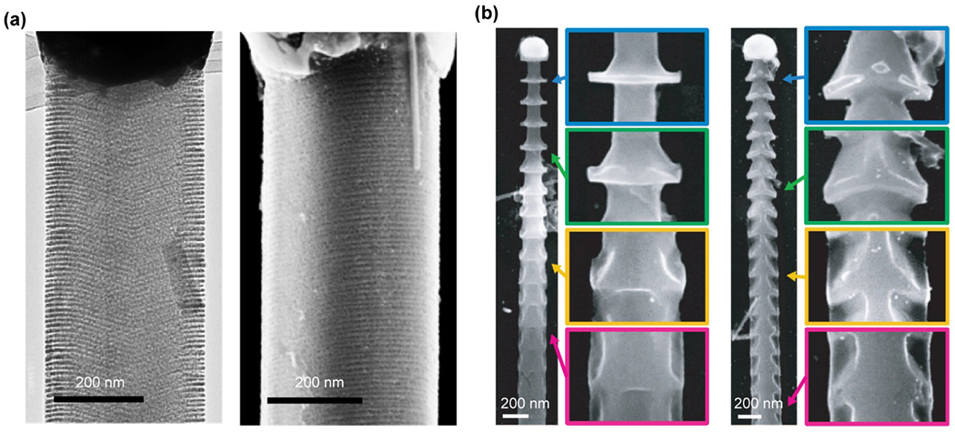
Si nanowires with various structures and morphologies can be produced from metal-assisted chemical etching methods. (a) SiNWs with ordered grooves, etched from a mixture of hydrofluoric acid/hydrogen peroxide. Reproduced from ref.143 under the terms of the Creative Commons Attribution License from Springer Nature, copyright 2017. (b) SiNWs spicules formed by wet chemical etching in KOH solutions. Reproduced from ref.144 with permission from the American Association for the Advancement of Science, copyright 2015.
Many other chemical etching methods, such as KOH etching or defect selective etching using solutions such as K2Cr2O7/HF or CrO3/HF, are also efficient routes for the fabrication of Si nanostructures.144–150 For example, anisotropic SiNW spicules were synthesized by wet chemical etching of p-doped SiNWs in KOH solutions (Fig. 4b), using atomic Au diffusion–induced patterns as the etch mask.144 An ENGRAVE (Encoded Nanowire Growth and Appearance through VLS and Etching) strategy was also developed to control the etching rate of Si in KOH using variable dopant concentrations.145–147 Specialized features ranging between 10 nm to 700 nm in length have been successfully encoded along the SiNWs.145–147
Finally, electrochemical etching allows for the synthesis of nanoporous Si films and particles from single-crystal Si substrates.139 The loose porous structures in electrochemically etched Si substantially reduced the Young’s modulus,67, 137 which is beneficial for establishing minimally invasive biointerfaces.
3.1.2. Degradation of Si-based structures
The physical and chemical properties of Si-based electronics are known to be very stable at dry states. But for bioelectronic applications, the degradation of Si at biointerfaces needs to be carefully considered in wet environments.151 Si reacts with water via hydrolysis to form silicic acid Si(OH)4: Si + 4H2O → Si(OH)4 + 2H2, where the Si(OH)4 departs the Si surface through diffusion. Silicon dioxide (SiO2) may also form as an intermediate.134 Several parameters play important roles in the degradation, including surface chemistry, dopants, pH, ion concentration and temperature.128, 152–155 Understanding the chemical processes of Si degradation has already opened a new way toward safer biomedical applications, e.g., in vivo implants based on transient electronics.125, 134, 156–159
Ultrathin single crystalline Si nanomembranes (SiNMs) are the main constituent in several well-performing, transient electronic systems. For example, Hwang et al. developed a transient integrated circuit by using degradable materials such as magnesium (Mg), MgO/SiO2, Si, and silk for parts like inductors, capacitors, and transistors (Fig. 5a).134 Si nanomembranes of 70 nm thickness were dissolved via hydrolysis with speeds of 4.5 nm/day and 2 nm/day under physiological temperatures (37°C) and room temperature (25°C), respectively. Magnesium coils, Si Joule heating elements, and silk substrates and packages conferred transient thermal protection against infection, as increased local temperature suppressed bacterial growth as well as eased pain. Similarly, Bai et al. developed injectable bioresorbable devices that can be naturally resorbed or undergo clearance from the body after an operational lifetime (Fig. 5b).160 This bioresorbable device can be successfully used for continuous checking of the cerebral microenvironment (i.e., temperature changes, oxygenation and neural activity) in freely moving mice. More recently, Shin et al. developed SiNM-based bioresorbable optical pressure sensors that depend on pressure-induced deflections of SiNM diaphragms (Fig. 5c).157 The potential of using this material, which is also compatible with magnetic resonance imaging (MRI), for clinical applications is very promising based on in vitro studies, histopathological evaluations, and acute measurements of intracranial pressure (ICP) and temperature (ICT).
Figure 5.
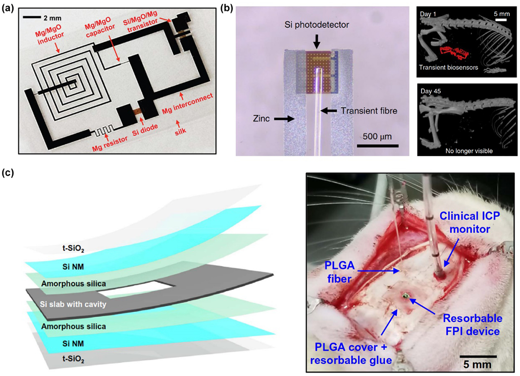
Transient and bioresorbable electronics derived from the degradation of Si and other transient materials. (a) Optical image of circuit design and components of a transient device. Reproduced from ref.134 with permission from the American Association for the Advancement of Science, copyright 2012. (b) Left: photograph of a SiNM-based bioresorbable spectrometer. Right: implanted device can be naturally resorbed after 45 days. Reproduced from ref.160 with permission from Springer Nature, copyright 2019. (c) Left: a schematic diagram of a SiNM-based bioresorbable sensor designed for the measurements of intracranial pressure (ICP) and temperature (ICT). Right: photograph of the bioresorbable sensor implanted in the intracranial space of a rat. Reproduced from ref.157 with permission from the American Association for the Advancement of Science, copyright 2019.
For long-term applications of Si-based bioelectronics,161, 162 degradation needs to be minimized. One technique for accomplishing this employs a thermal oxide thin layer directly grown on the surface, which can prevent biodegradation in phosphate-buffered saline solution.163 Several efficient passivation coating materials also work well to inhibit Si degradations, including stable Al2O3,162 TiO2,164 and SrTiO3.165 As demonstrated by Hu et al., atomic layer deposition (ALD) of TiO2 layer (4 to 143 nm thick) significantly improves the stability of Si photoanodes under basic water oxidation conditions.161 More generally, TiO2 stabilizes many semiconductors during oxidative photochemical processes by engineering the band structures and the defect states.
3.1.3. Chemistry for optical functionalities at the Si biointerfaces
Among the many useful functions of Si semiconductors, their ability to convert light into electric current is one of the most important uses. After Si semiconductors absorb light, the photonic energy can be transferred into electronic energy. When Si-based materials are used in cell cultures or as implants, they are usually surrounded by biological fluids, forming semiconductor/saline interfaces. With light, this can yield transient, photocapacitive modulation of cells or tissues (Fig. 3), or longer-lasting photofaradic reactions (Fig. 3) where the electrons and holes participate in cathodic and anodic reactions, respectively.
Palanker et al. developed a series of photovoltaic retinal implants, where the high-pixel-density devices provide local modulation of rat retinal neurons for potential restoration of vision.166–168 In order to enhance photostimulation by nano-bioelectronic devices, the photovoltaic or photoelectrochemical effect must be maximized. Parameswaran et al. found that dopant modulation and surface chemistry of the Si nanostructures could enhance their performance as neuromodulators (Fig. 6a).129 They used coaxial p-type/intrinsic/n-type (p-i-n) SiNWs, each consisting of a p-doped core nanowire, an interlayer of intrinsic Si, and a n-doped shell, to modulate primary rat dorsal root ganglion (DRG) neurons through photoelectrochemical processes. Experiments also showed that diffused atomic Au on the SiNW sidewalls could significantly enhance the generation of photoelectrochemical currents, and thus the neuromodulation efficacy (Fig. 6b).129 A similar conclusion was found in another study conducted by Jiang et al., which studied 2D p-i-n Si membranes with noble metal nanoparticles (e.g., Au, Ag and Pt) decorated on their surfaces by means of an electroless deposition method.38 They found that metal-decorated p-i-n membranes enhanced photoelectrochemical current generation by at least an order of magnitude. This successfully yielded photo stimulation of the brain cortex and behavior control (Fig. 6c).38 Si photovoltaic devices can also play a key role in ultrasensitive detection of biometric signals. Yokota et al. recently reported the fabrication of a conformable imager derived from low-temperature polycrystalline Si (LTPS) thin-film transistor (TFT), which can read out small photocurrents of less than 10 pA with low noise.169 The TFT readout circuits are designed by Si oxide film (SiO), Si nitride film (SiN), and amorphous Si film (a-Si) that was transferred from polycrystalline Si through excimer laser annealing. Combined with sensitive organic detectors, the imager can detect and calibrate the displacement of the device electronically on the basis of fingerprint or vein feature points.
Figure 6.
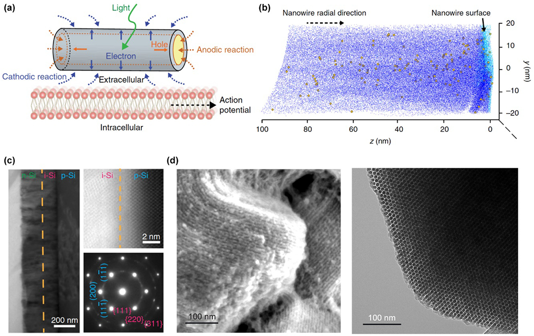
Si nanostructures used in the photo stimulation of cells. (a) A schematic diagram shows coaxial p-type/intrinsic/n-type (p-i-n) SiNWs for photoelectrochemical extracellular modulation of DRG neuron membrane potential. (b) Atom probe tomography shows the presence of diffused Au (yellow balls) on the sidewalls of p-i-n SiNWs (Si atoms: dark blur; O atoms: light blue). (a) and (b) Reproduced from ref.129 with permission from Springer Nature, copyright 2018. (c) Cross-section TEM image (left), scanning TEM (STEM) image (upper right) and the diffraction pattern of a p-i-n Si membrane nanostructure applied for the photostimulation of brain cortex and behavior control. Reproduced from ref.38 with permission from Springer Nature, copyright 2018. (d) Left: SEM image of nanostructures of replica Si from hexagonal mesoporous silica SBA-15, which were applied in the elicitation of action potential by photothermal effect. Right: TEM image shows the hexagonal packing of a Si nanowire. Reproduced from ref.67 with permission from Springer Nature, copyright 2016.
Electric energy generated from light radiation on Si can also be converted into heat, in a process known as the photothermal effect as described in section 2.3.4 (Fig. 3). The local temperature increase induced by light can be exploited to activate biological responses. This is a promising avenue for Si-based photostimulation. Researchers have developed strategies to enhance this Si photothermal effect. Jiang et al, developed mesoporous Si microparticles with a nano-casting method (Fig. 6d).67 The replica Si from hexagonal mesoporous silica SBA-15 display open-framework and porosity. The microparticles have an improved photothermal effect, as the porosity reduces the thermal conductivity and heat capacity but enhanced the light absorption. This mesoporous Si can modulate action potential (AP) firing and deterministic neuronal responses up to ~15 Hz through an optocapacitance mechanism.67
3.1.4. Chemistry for electrical functionalities at the Si biointerfaces
One of the most common applications for semiconductor-based bioelectronics is sensing bioelectrical signals. While patch-clamp electrodes have been developed enough that they can sense localized electrical signals from single ion channels, the electrodes are invasive and the biointerface is brief. With a smaller dimensionality, SiNW-based nano-bioelectronics43, 170–172 have been developed for intracellular recordings.43 The chemical designs of the SiNWs play a key role in facilitating the intracellular entrance. For example, the first nanoscale FETs (nanoFETs) used for intracellular electrical recording involved the CVD synthesis of kinked nanowires with dopant modulation. The kinked SiNWs with two cis-linked kinks of an overall ~60° angle of the bent junction were achieved by repeated pressure modulations (Fig. 7a–c).43 The nano-sized FET region was established by inserting a lightly doped region (~200 nm) in heavily doped n-type nanowire backbone (Fig. 7a). Such doping control enables a localized FET region for sensitive intracellular recording. 43
Figure 7.
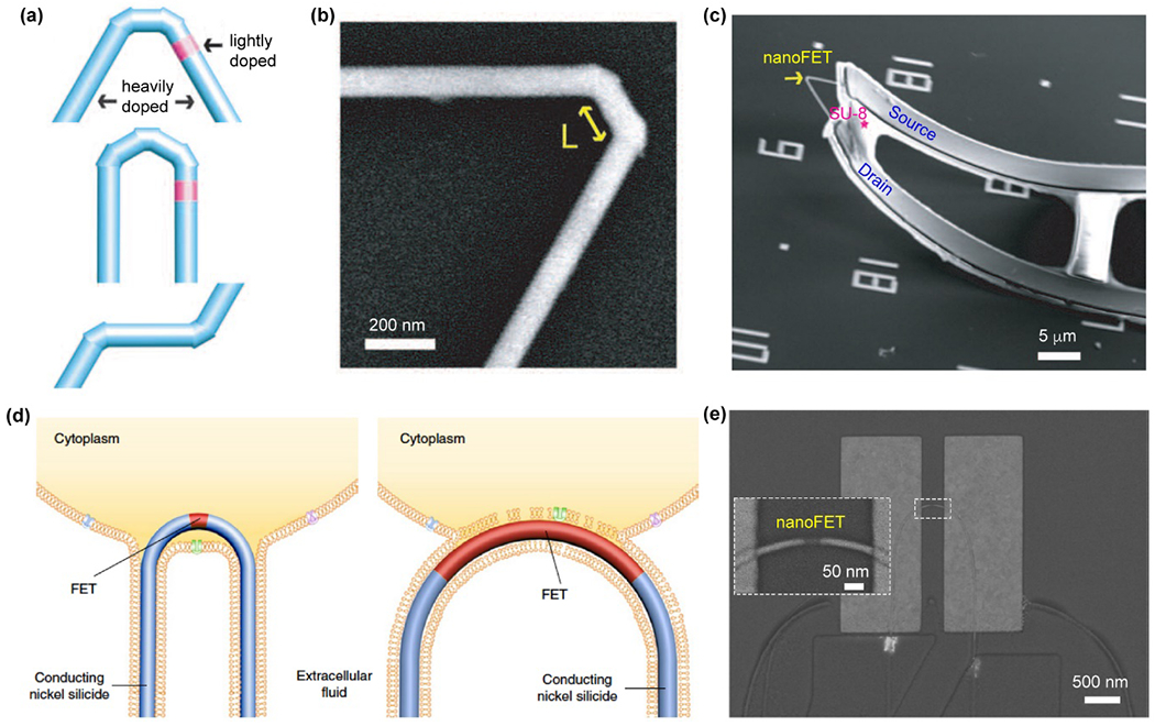
Si-based nanoFET for intracellular recordings. (a) A schematic diagram of the nano-sized FET region, which was introduced by dopant modulation on kinked nanowires. (b) A SEM image of a kinked Si nanowire. (c) NanoFET on an SU-8 microribbon support. (a) – (c) Reproduced from ref.43 with permission from the American Association for the Advancement of Science, copyright 2010. (d) A schematic diagram of probe internalization and intracellular recording by short channel nanoFETs. (e) SEM image of a U-shape nanoFET with atomically sharp nickel silicide interfaces. (d) and (e) Reproduced from ref.175 with permission from Springer Nature, copyright 2019.
Atomically sharp nickel silicide interfaces derived from solid-state reactions on Si nanowires yielded short-channel nanoFET devices.173 Using this method, Zhao et al. realized a scaleable fabrication of highly sensitive nano-bioelectronics (Fig. 7d and e) through deterministic shape-controlled nanowire assembly.174, 175 These devices were able to record the full amplitude APs from primary neurons and other electrogenic cells in a multiplexed layout.
Additionally, the Rogers group has developed a series of works about the thermal growth of SiO2 layers over Si nanomembranes. This oxide design not only enabled the electrical coupling of devices to tissues, but also served as an encapsulating material against the penetration of biofluids. These bioelectronic devices showed safe and long-term applicability, including epicardial mapping of ex vivo hearts and electrical stimulation.176–178
Lastly, molecular functionalization of silicon surfaces has been widely applied to improve the electrical performance of silicon substrates in biosensing applications and memory devices.179 H-terminated silicon surface can be directly or indirectly coupled with electrically active moieties via oxide-free functionalization. Such moieties include but are not limited to ferrocene,180–182 quinones,183 metal-complexed porphyrins,184 tetrathiafulvalene (TTF),185, 186 and fullerene (C60).187, 188 Additionally, Bunimovich et al. reported FET-based biosensors with oxide-free Si–C layers that showed exceptional sensitivity (< 0.1×10⁻⁹ M) in DNA detection,189 where single-stranded DNA was electrostatically adsorbed. Changes of molecular length, packing density, and coverage in surface terminating groups can largely influence insulating properties and capacitance performance.180, 190–192
3.1.5. Chemistry for tight integration at Si biointerfaces
Overall, molecules with a variety of terminal groups can be anchored directly onto silicon surfaces via covalent bonds, e.g., silicon-carbon, silicon-nitrogen, and silicon-oxygen bonds. The resultant properties strongly depend on the surface molecular layer formation processes, which include carbonization, oxidation, hydrolytic condensation, thermal dehydrocoupling, and ring-opening click chemistry.193, 194 The functionalized surface monolayer further serves to provide linkages that are useful for attachment of native bioderivatives (e.g., peptide motifs195, 196 and proteins197–200) and synthetic nanomaterials.201 When immobilized on the silicon surfaces, these species can effectively improve cell-silicon interactions or biosensing abilities.89, 202
Si surface chemistry plays an important role in the interaction between Si-based materials and biological targets. For example, surface modifications of Si substrates with polylysine can be used for deterministic patterning of Si/neurite interfaces.203 Surface modification can also enable controlled cellular internalization of SiNWs. Zhang et al. reported strong interactions between SiNWs modified with folate and CHO-β cells, and uptake of the modified SiNWs by the cells.204 Surface coating of SiNWs has also facilitated intracellular recording. The Lieber group has reported several cases which showed that surface modification of SiNW-based nanoFET probes with a phospholipid bilayer can promote intracellular entrance for the device through a possible membrane fusion process.42, 43, 175
Surface geometry modification can also help establish close biological integration. For example, through Au diffusion in SiNW growth and subsequent wet-chemical etching, Luo et al. reported the synthesis of anisotropic Si spicules (Fig. 4b). With a spiky sidewall, the spicules established very strong mechanical interactions with extracellular matrix materials, such as a collagen hydrogel144. Similar structural features may be adopted for future implantable material design and implementation.
3.2. Other inorganic semiconductor-based materials
Besides Si, inorganic semiconductors such as ZnS nanoparticles, TiO2 nanotubes, MoS2 nanosheets, and many other metal oxides and metal sulfides have also been widely used in bioelectronics or bioelectrical studies. Their stability, diverse band gaps, and broad range of nanostructures make them good candidates for chemical and biological sensing, in vitro or in vivo labeling, and energy transduction at biointerfaces.205–208
3.2.1. General synthesis methods
Here we discuss a number of methods for synthesizing semiconductors that are tailored to fit the eventual biological question or application for the materials. The four processes we focus on are gas phase, solution phase colloidal, electrodeposition/molten salt-enabled, and bioinspired mineralization syntheses. These techniques allow for a vast array of possible compositions and device geometries, depending on the specific needs of the biointerface with respect to parameters such as band gap, size, and toxicity. For instance, interfaces intended to be used with photoelectrochemical modulation work best with bandgaps in the visible light range.
a). Gas phase synthesis
Conventional epitaxial growth methods of semiconductor thin films include molecular beam epitaxy (MBE), pulsed laser deposition (PLD), and CVD.209 The MBE method could precisely control the growth process at the atomic level. However, ultrahigh-vacuum (<10−10 torr) conditions are required. PLD requires a low-pressure system in the presence of precursor gases such as O2, N2 and H2 and is good at creating artificially layered oxides for fabrication of oxide electronic and magnetic materials. CVD and metal-organic chemical vapour deposition (MOCVD) are most commonly used methods for semiconductor thin film epitaxial growth. Various kinds of semiconductor thin films, such as MoS2,210 WS2,211 WSe2,212 SiGe,213 GaAs,214 InGaP,215 and GaN216 have been synthesized from the CVD or MOCVD methods.123, 205, 217 Semiconductor thin films with single-atom thickness and unique electronic band structures provide key advantages in developing novel electronic and photonic devices.218 Compared with other synthesis methods, the precise control over chemical composition, the high-quality crystalline nature, and the low defect level of semiconductor thin films ensure excellent electrical and optical properties across the entire materials.208 Additionally, CVD and MOCVD syntheses can produce bulky chips and circuits for future large-scale bioelectronic applications.
b). Solution phase colloidal synthesis
There are a variety of solution-based methods available, including sol–gel process, co-precipitation, thermal decomposition, and hydrothermal method. The sol–gel process, i.e., hydrolysis and polycondensation of metal alkoxide (or halide)-based precursors, has been applied to synthesize nanocrystalline or amorphous semiconductors. For making nanocrystals with a narrow size distribution, co-precipitation is widely used, as its lack of extra calcination and post-annealing steps make it more convenient. Polyvinylpyrrolidone (PVP), polyethylenimine (PEI), and other capping molecules have been used for tailoring the particle nucleation and growth kinetics and for stabilizing nanocrystals. Solution-phase methods provide a variety of synthetic combinations for different structural and compositional features. Furthermore, dopants enable tuneable electronic and photonic properties to meet desired specific requirements at biointerfaces.219
c). Electrodeposition/molten salt method
GaAs, GaP, InP, and GaInP2, can also be synthesized using electrodeposition in plating solutions.220 For example, GaAs can be co-deposited by Ga(III) and As(III) oxides (e.g., H3AsO3, HAsO32−) through high temperature reduction and sequential room temperature aqueous solution deposition. Because the as-deposited semiconductors are usually amorphous or poorly crystallized, further annealing processes are frequently required. Electrodeposition of GaP or InP is usually completed by melting eutectics, e.g., NaF/NaPO3/Ga2O3 or In2O3/NaPO3/KPO3/NaF/KF salts at about 600-900 °C. Alternately, a two-step method involving cathodic electrodeposition of In, followed by post-deposition phosphorization with red phosphorus also resulted in the synthesis of InP.
d). Bioinspired mineralization processes
Ion exchange methods developed by Holtus et al. have demonstrated the successful transformation of carbonate minerals into perovskite semiconductors.221 This method can be used to produce 3D structures with tuneable bandgaps, without significant changes to the overall morphology of the material. This raises the possibility of combinatorial investigations into biointerface formation, where the material structure remains consistent, but the electrical parameters of the material vary.
3.2.2. Quantum dots-based bioelectrical studies
The photoluminescence of semiconductor materials, especially for quantum dots, has been widely used for cell and tissue imaging.154, 222 They are used to track organelle or cell dynamics upon electrical modulation or for correlative bioelectronic sensing and imaging. Quantum dots have been demonstrated to be nanosized tools which can efficiently record subthreshold and suprathreshold events. In particular, detecting bioelectrical events in the space between two lipid layers of the cell membrane (Fig. 3) has been proposed and demonstrated preliminarily,223–225 which is challenging for electrode recording methods. By coupling quantum dots with other molecular systems, bioelectrical sensing in neural membranes can also be conducted. For example, Nag et al. reported using CdSe/CdS/ZnS QD for electric field-sensitive charge transfer and for mapping membrane potential in living cells (Fig. 8).225 They designed a QD (electron donor) – peptide/fullerene (electron acceptor) bioconjugated system, where hydrophilic QDs were localized at exofacial leaflets of the plasma membrane while multiple copies of hydrophobic peptide–C60 fullerenes self-assembled within the lipid bilayer.225 Upon membrane depolarization, electrons transfer with enhanced basal rate from the photoexcited QD donor to the fullerene acceptor, giving rise to further quenching of QD/PL. The fluorescence response of this integrated bioelectrical probe exhibits comparable temporal responsiveness, but with 20- to 40-fold greater normalized change in fluorescence values than those reported for voltage-sensitive dyes.
Figure 8.
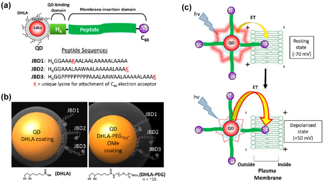
QD applied for bioelectronic voltage sensing in neural membranes. (a) A schematic diagram and (b) molecular models for the design of the QD (electron donor) – peptide-fullerene (electron acceptor) bioconjugated system. (c) A schematic diagram for the fluorescence change introduced by membrane depolarization process. The electrons transfer from the photoexcited QD donor to the fullerene acceptor when the plasma membrane is depolarized, giving rise to the quenching of PL. Reproduced from ref.225 with permission from the American Chemical Society, copyright 2017.
Moreover, the nanoscale sizes of QDs have enabled light-triggered redox reactivity in the cytosolic space from the subcellular biointerfaces. This has produced light-harvesting bacteria and yeast cells for energy-efficient biofuel or fine chemical production, a new approach in synthetic biology and biomanufacturing.226–230
Finally, the emission from QDs can be used for optogenetics stimulation. A notable example is a recent demonstration of using ZnS-based mechanoluminescent QDs for ultrasound-triggered optogenetics231. The photoexcited QDs were injected into the blood circulation and can be recharged by 400 nm light at the superficial vessel location. The QDs emit light on-demand by applying a focused ultrasound through intact scalp and skull. This demonstration opens up a new avenue for future in vivo bioelectrical studies with QDs.
3.2.3. 2D-semiconductors bioelectronics
2D semiconductors such as MoS2226–229, just a few nanometres in thickness, are good candidates for soft bioelectronics.232 The band gap of monolayer MoS2 is 1.8 eV and 1.2 eV for the bulk.233 MoS2-based FET devices have a high on/off ratio,205, 234 together with high surface-to-volume ratio, which makes them highly suitable for bioelectronic sensing.123, 213 Sarkar et al. reported a MoS2-based FET sensor that can detect streptavidin at ultralow concentrations, about 100 fM.232 Additionally, the flexibility and the piezoresistivity of MoS2235 have enable the fabrication of a skin-like tactile sensor array, as reported by Park et al.236 This MoS2-based conformal tactile sensor can be placed over uncommon surfaces such as leather and a human fingertip. The device showed sensitive and robust behaviors and linear responses even after 10,000 loading cycles.
2D semiconductors also possess advantages for optoelectronic applications due to their excellent absorption in the visible range and the capability to generate photocurrent. For example, Choi et al. reported the design of a human eye-inspired, hemispheric image sensor with high array density, which was fabricated from a MoS2-graphene heterostructure.237 These soft implantable bioelectronics act as retinal prosthetics and can successfully stimulate optic neuronal cells of a rat under external optical irradiation. Furthermore, MoS2 demonstrates high rates of electron-hole pair generation in response to illumination. Liu et al. reported that the reactive oxygen species (ROS) generated from the photocatalysis effect of few-layered vertically aligned MoS2 achieved E. coli disinfection with >99.999% inactivation.236 Photoexcited electron–hole pairs in other semiconductor composites,238, 239 such as C3N4/rGO heterojunctions,240 may also enable the photocatalytic effect in cells and tissue. Zhang et al. reported a modulation neuronal interface between C3N4 and PC12 cells, where neuronal differentiation can be achieved upon photostimulation.240 Moreover, the photocatalytic effect has enabled g-C3N4 mediated conversion of NADH into NAD+, a process which can be utilized for the catalytic synthesis of L-lactate from L-lactate dehydrogenase.241–243
The shape, dimensions, chemical composition, and surface properties of 2D semiconductors are all related to their biocompatibility. While 2D MoS2 has been demonstrated to show low cytotoxicity,244, 245 biocompatibility in vitro and in vivo remains a concern for other 2D materials, especially for those transition metal dichalcogenides containing Se, Te, or As.246–248
3.2.4. Metal oxide-based bioelectronics
Many metal oxide semiconductors can be configured as FET devices. For example, Nakatsuka et al. used thin-film In2O3 FETs for biomolecular sensing under physiological condition. They modified their FETs with DNA aptamers whose conformation changes upon binding to various molecules such as serotonin, dopamine, glucose and sphingosine-1-phosphate. Notably, the detected molecular concentration ranges from 10−14 to 10−9 M in PBS solution, overcoming the limitations of Debye screening .249
Metal oxide semiconductors are also frequently applied as photocatalysts and solar-to-chemical energy conversion materials because of their inherent ability to generate electron and holes upon photoexcitation, good charge carrier mobility, excellent stability, and tuneable structures. TiO2 is one of the most frequently used materials for in vitro and in vivo bioelectronic applications. Demonstrated by Tang et al., a vertically oriented Au-decorated TiO2 nanowire array of artificial photoreceptors successfully restored functional and behavioral light sensitivity in blind mice.250 This nanowire array resembles the architecture and function of photoreceptors in retinas. Unlike other engineered bioelectrical implants for sight restoration, TiO2 arrays require no trans-ocular cables or power supplies and are expected to offer optimized spatial resolution. With Au nanoparticle decoration, surface roughness guarantees enhanced interfacing between innate retinal circuits and TiO2. Design of future retinal implants or bioinspired devices would need materials with broadband photo-responsivity from the UV region to the near-infrared region, for which oxide composites or doped oxides may meet the requirement (e.g., Au-WO3-TiO2,251 CuO/Ta2O5,252 or In-doped TiO2253). Other example in this category includes niobium oxide (Nb2O5)-based photoelectrochemical sensing.254
Many metal oxides, such as tantalum pentoxide (Ta2O5), ruthenium oxide (RuO2), nickel oxide (NiO), manganese dioxide (MnO2), and cobalt oxide (Co3O4) are widely applied as electrode materials in lithium-ion batteries, supercapacitors, and solar cells;255,256 the device configurations and operational mechanisms can be tailored for bioelectronics more broadly. Most of these metal oxides can be obtained through hydrothermal synthesis to yield controllable shapes and electrochemical or optical properties.
4. Organic semiconductor-based bioelectronics
Organic semiconductors have become excellent candidates for flexible and stretchable bioelectronic applications, because of their low temperature solution-phase processability, good mechanical deformability, and applicable charge transport properties.39, 257 When in contact with skin or implanted into tissues, mechanically compliant organic bioelectronics can minimize discomfort and adverse effects due to the mechanical mismatch.39, 257–260 Moreover, some organic semiconductors are self-healable and biodegradable, which is ideal for wearable and injectable bioelectronics.261, 262 However, several factors, including the balance between mechanical deformability and device mobility, long-term stability under physiological conditions, stretching and bending durability, need to be considered during the development of the next generation of organic bioelectronics. In this section, we discuss the molecular design of semiconductor polymers, chemical and biochemical sensing from organic transistors, surface chemistry for targeting, photoelectrochemistry and photochemistry of organic semiconductors, and energy conversions of organic semiconductors used in bioelectronics.
4.1. Chemical designs for mechanical deformability
Rational design of semiconductor polymers can help improve the mechanical properties without negative changes to the electrical transport behaviors.263–266 Increasing the size or number of amorphous regions by lowering regioregularity could prevent crystallization in semiconductor polymers. This would lead to an increase of stretchability, however, it also impacts the electrical performance.267 Side chain engineering of semiconductor polymers is another efficient route for modulating stretchability.267 For example, the linear alkyl side chain modification of poly(3-alkylthiophene) (P3AT) developed by Savagatrup et al.268 and poly(butyl acrylate) (PBA) side chain modification of isoindigo-based polymers PII2T developed by Wen et al.269 showed that the tensile moduli of such polymers can be reduced by softening the side chains.
Recently, the introduction of conjugation breaking spacers (CBs) into the backbone was demonstrated to be an efficient strategy to endow stretchability to the semiconductor polymer.270–272 Oh et al. reported the creation of 2,6-pyridine dicarboxamide (PDCA) conjugation units that integrated with 3,6-di(thiophen-2-yl)-2,5-dihydropyrrolo[3,4-c]pyrrole-1,4-dione (DPP) semiconductor polymers (Fig. 9).273 PDCA moieties introduce hydrogen bonding units into the polymer backbone. While the semiconducting crystalline parts allow remarkable charge transport, amorphous polymer chains crosslinked by hydrogen bonds – which can reversibly undergo dynamic breakage and reformation – offer the polymers excellent flexibility and tolerance to stretching. Organic thin-film field effect transistors (OTFTs) fabricated using this intrinsically stretchable semiconductor can be stretched without significantly compromising the semiconducting behavior, with only a slow decline in field effect mobility when stretched up to 100%. When mounted on human limbs, this OTFT device can tolerate various human movements such as arm folding, hand twisting, and elbow stretching, while retaining an average mobility bigger than 0.1 cm2⋅V−1⋅s−1.
Figure 9.
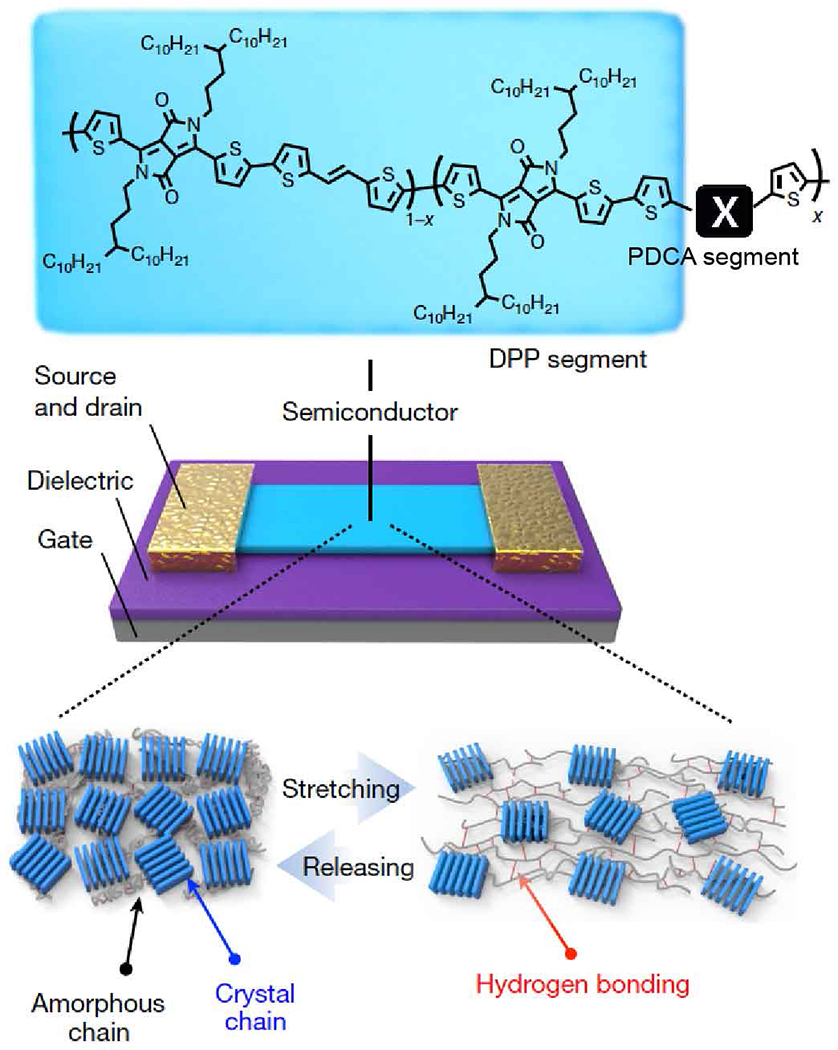
Intrinsically stretchable and healable polymers for fabricating stretchable organic thin-film field effect transistors (OTFTs). 2,6-pyridine dicarboxamide (PDCA) conjugation breaking spacers are integrated with the 3,6-di(thiophen-2-yl)-2,5-dihydropyrrolo[3,4-c]pyrrole-1,4-dione (DPP) semiconductor polymer. The polymer contains crystalline domains (blue) and amorphous polymer chains, where dynamic hydrogen bonds can break and reform. Reproduced from ref.273 with permission from Springer Nature, copyright 2016.
4.2. Chemical designs for degradation and stability
Organic semiconductor-based bioelectronic devices are typically not as stable as their inorganic counterparts. Depending on the intended purpose of the device, specifically the duration of the interface, this can be either a positive or negative aspect.
There are two major routes for the degradation of semiconductor polymers: hydrolytic degradation and oxidative degradation.274 Hydrolytic degradation is determined by the microstructure and composition of the polymer, as well as the temperature and pH of the surroundings. For hydrolytic degradation, several kinds of sites on the polymer backbone can initiate chemical and enzymatic degradation, including ester/thioester, carbonate, anhydride, urea, urethane, and imide/amide groups, etc.274 An increase of crystallinity and cross-linking density would typically lead to a decrease of degradation rate. Oxidative degradation is a chemically and enzymatically relevant oxidative cleavage procedure of polymers. Common sites for oxidative degradation in polymers are shown in reference.274
For long-term bioelectronic devices, stable performance is required (e.g., organic photovoltaic components used as a retinal prosthesis). Encapsulation of the device to prevent water and oxygen transmission is an efficient strategy. For example, in organic LED (OLED) synthesis, the semiconductor polymer can be protected by a ~1 μm thick multilayer encapsulation.275 The encapsulation contains three layers of Al2O3 and two layers of crosslinked acrylic polymer, complying with the standards for typical encapsulation of OLED microdisplays. This multilayer structure encapsulating effect is 10−5 –10−6 g⋅m−2⋅d−1, which is comparable with low water vapor transmission rates. Rational design of the polymer structure is another efficient strategy to improve stability.276 For example, Giovannitti et al. reported that 3,3′-dimethoxy-2,2′-bithiophene comonomers in alkoxy-Benzo[1,2-b:4,5-b′]dithiophene (BDT) copolymers improved the material stability.277 Specifically, they found that alkoxybithiophene units stabilize positive charges on the polymer backbone, playing a vital role in the long-term operation of OECT.
In some biomedical applications, transient bioelectronics are useful for in vivo healing or regeneration,153, 261 as was discussed in section 2. Nondegradable implants may create a risk of causing a chronic inflammation, necessitating extra surgeries to take them out which risks infection. Thus, molecular designs that make organic semiconductor-based devices degradable at physiological conditions are desirable. For example, Lei et al. utilized imine-linked DPP and p-phenylenediamine to synthesize degradable organic materials in acidic (pH = 4.6) environments.278 By coupling this material with iron electrodes, they fabricated ultra-lightweight disintegrable pseudo-CMOS logic circuits and polymer transient electronics. Their biodegradable organic semiconductor electronics have the potential use for biointegrated applications.
4.3. Chemical designs for electronic functionalities
Organic semiconductors have been developed for numerous bioelectronic applications, notably the skin-inspired electronics.279, 280 For example, transistor-matrix based organic electronics with thousands of flexible sensory units can potentially replicate skin sensation.270 Wang et al. developed a large-scale high yield uniform transistor array with an intrinsic stretchability up to 100% strain while keeping a ~1 cm2⋅V−1⋅s−1 charge-carrier mobility.259 Kim et al. configured organic transistors into artificial synaptic junctions,279 where the active channels in an ion gel can be gated by multiple inputs. A hybrid monosynaptic reflex arc was demonstrated by connecting this artificial synaptic transistor to nerves of a discoid cockroach.
4.3.1. Chemical designs for charge carrier mobility control
Rational design of semiconductor polymers is the efficient route for improving carrier mobility while keeping good mechanical properties.263, 265, 266 The crystalline domains in semiconductor polymers, which arise from intermolecular π-π stacking, are favourable for charge carrier mobility.271 Thus, molecular weight plays an important role in charge carrier mobility.281 Zen et al. reported that in the case of poly(3-hexylthiophene), abbreviated as P3HT, high molecular weight P3HT has higher mobility in organic field-effect transistors,282 which rely on tie chains with connection function and effective charge transportation between crystalline regions. However, high molecular-weight P3HT showed a lower elastic modulus. More recently, new molecular design routes have been developed for less crystalline polymers to achieve both the high charge mobility and stretchability. For example, Xu et al. used a nanoconfinement method to increase polymer chain dynamics and suppress crystallization, while maintaining the mechanical properties of high-mobility polymers.270, 271 When introducing nanofibrils into a soft deformable elastomer, semiconducting films can be stretched to 100% strain without influencing mobility.
4.3.2. Surface chemistry in organic transistors
Two kinds of transistors, including organic electrochemical transistors95, 283–285 (OECTs, based on electrochemically doping/de-doping upon ionic species injection into the active materials) and electrolyte-gated organic field effect transistors286–288(EGOFETs, based on gate voltage-modulated channel currents via a capacitive field effect mechanism at the channel/electrolyte interface) are commonly used in bioelectronic sensing. For detailed information regarding the working principles of these devices, we refer the interested reader to a number of excellent reviews on the subject.26, 95, 289
Surface modifications with functional chemical moieties, peptides, proteins, and nucleic acids enable specific chemical and biological detection with high sensitivity.290–292 For example, the Inal and Owens groups have conducted extensive research on surface biofunctionalization of OECT devices.290, 293–295 Several enzymes, including glucose oxidase (GOx), lactate oxidase (LOx), and cholesterol oxidase (ChOx), were covalently immobilized onto the PEDOT:PSS gate electrodes to enhance the sensing selectivity.290 For instance, the PEDOT:PSS can be blended with polyvinyl alcohol (PVA) to introduce hydroxyl functional groups, and then linked with heterobifunctional silanes, i.e., 3-glycidoxypropyltrimethoxysilane or GPTMS, via a condensation reaction prior to the protein attachments. Containing an epoxy ring, this silane can form chemical bonds with amides from target proteins. The OECT device is based on the n-type copolymer P-90 with lactate oxidase grafting. Working as a resistor, the LOx-functionalized micro-channel amplified the signal of the transistor circuit with its current changing near the noise level with lactate.
Biorecognition can also be realized by surface functionalization (Fig. 10a and b).294 Mulla et al. employed monomeric porcine odorant binding proteins (pOBPs) as ligands and assembled them on the metal gate of a capacitive coupled p-type organic FET (polymer, PBTTT-C14) device.291 This device can be used for the selective detection of chiral differential interaction in OBPs in the picomolar concentration range (Fig. 10c and d). Subtle capacitance changes that associated with the ligand-protein complex formation allow sensitive determination of the free-energy balances from conformational events, i.e., the interaction of chiral (S)-(+)- and (R)-(−)-carvone enantiomers with OBPs. While pOBPs are negatively charged in pure water, the chiral molecules bear a dipole moment and physically bind to pOBPs.
Figure 10.
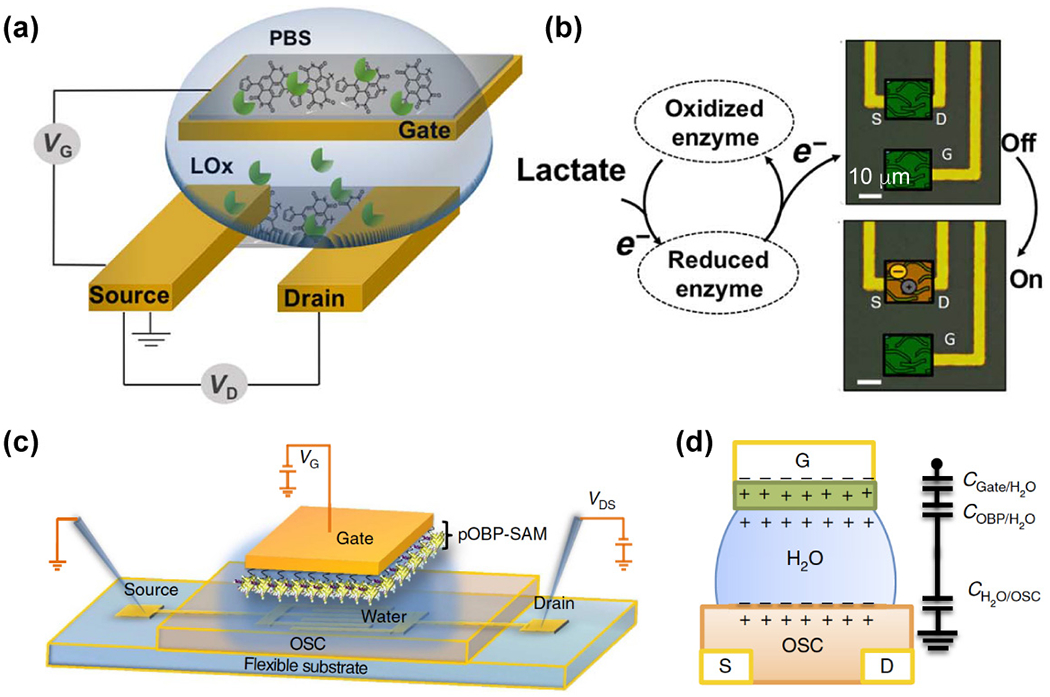
Surface modification of organic transistors for bioelectronic sensing. (a) A schematic diagram of the enzyme biofunctionalization on OECTs devices. (b) LOx enzyme immobilized on the gate electrode of transistors can enhance the sensing selectivity. (a) and (b) Reproduced from ref.294 with permission from the American Association for the Advancement of Science, copyright 2018. (c) A schematic diagram and (d) working mechanism of a capacitively coupled p-type organic FET with pOBPs as ligands. (c) and (d) Reproduced from ref.291 under the terms of the Creative Commons Attribution License from Springer Nature, copyright 2015.
Different to chemical conjugation, physical adsorption process depends on binding kinetics and equilibrium and can be driven by surface energy, intermolecular forces, polarity, charges, and morphology.296–298 The desire to understand how these factors impact protein adsorption and to predict and control the adsorption process have been main motivating forces for the research in this field, which can help optimize engineering techniques performance in biomedical or physiological applications.299
4.3.3. Photoelectrochemistry of organic semiconductor-based biointerfaces
Organic semiconductors can also be utilized in light-triggered electron injection or stimulation. Capacitive processes from double layers and Faradaic process from reduction/oxidation of a solution species, as discussed in section 2.3.2, are the two main processes that occur at liquid/solid interfaces. Applying photostimulation strategies on the biointerface, such as optical neuronal modulation,300 presents a potential future direction for biomedical implants as brain disease therapeutics or retinal prostheses.301–304 Due to the mechanical deformability properties of polymers, organic semiconductors are ideal for injectable and implantable bioelectronics.305–307 Meanwhile, organic semiconductors may also produce electron-hole pairs upon exposure to sufficiently energetic light. This capability for photostimulation may be further enhanced by the good charge carrier mobility available in organic semiconductors.98, 305, 308–315
Ghezzi et al. reported that by employing semiconductor polymer regioregular poly(3-hexylthiophene-2,5-diyl) with phenyl-C61-butyric-acid-methyl ester (rr-P3HT:PCBM) as a photosensitive layer, and ITO as a reference electrode, hippocampal neurons cells could be photostimulated through a photovoltaic mode.309 Maya-Vetencourt et al. developed an organic implant for restorative retinal prostheses using a similar method.308 They utilized P3HT as an active semiconductor layer, poly(3,4-ethylenedioxythiophene): polystyrene sulfonate (PEDOT:PSS) as intermediate conductive layer, and 30 μm thick silk fibroin layer as a passive substrate (Fig. 11a).308 After implantation, this biocompatible and photosensitive organic prosthetic can rescue light sensitivity and spatial acuity in vivo for nearly a year. Additionally, a P3HT-based optoelectronic epiretinal interface was reported by Gautam et al. to provide visual cues that could stimulate blind retina.
Figure 11.
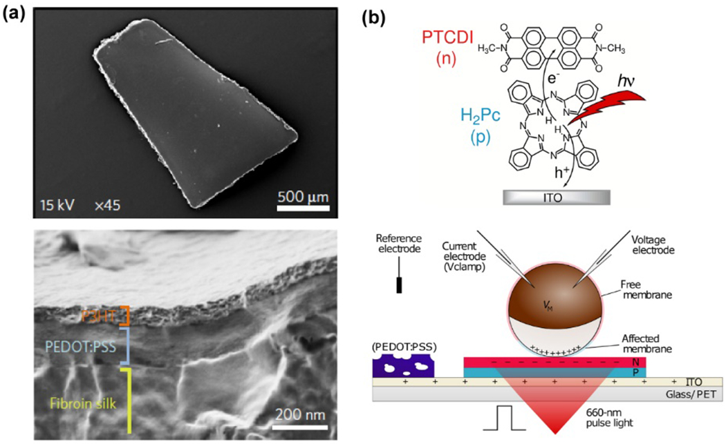
Organic semiconductors used for optical modulation of cells and tissues. (a) SEM images of photosensitive organic prosthetic implants composed of active P3HT layer, conductive PEDOT:PSS layer, and silk fibroin substrate. Reproduced from ref.308 with permission from Springer Nature, copyright 2017. (b) A schematic diagram of the organic electrolytic photocapacitors based on H2Pc / PTCDI junction for the X. laevis oocyte photoexcitation. Reproduced from ref.317 with permission from the American Association for the Advancement of Science, copyright 2019.
Jakešová et al. demonstrated that organic electrolytic photocapacitors (OEPCs)316 could be used to generate photocapacitive current for X. laevis oocyte stimulation.317 Photoexcitation of the H2Pc (P-layer, donor) and PTCDI (N-layer, acceptor) junction accumulated electronic charges, forming the opposite electrolytic double layer at the front and back plane of semiconductor electrodes (Fig. 11b).317 Furthermore, organic photovoltaic photosensors of (2,4-bis[4-(N,N-diisobutylamino)-2,6-dihydroxyphenyl] squaraine, (SQIB) blended with a fullerene acceptor (phenyl-C61-butyric acid methyl ester, PCBM) were utilized by Abdullaeva et al., to examine how activation of voltage-gated ion channels works in single neuroblastoma (N2A) cells by utilizing patch-clamp recording.318
4.3.4. Other organic semiconductors devices relevant for biointerfaces
Organic semiconductors may serve as energy transducers, converting solar energy to electrical energy (organic photovoltaics, OPVs). Thus, organic semiconductor-based devices can be employed as a power and light source in various kinds of biomedical applications.319–321 Park et al. created a self-powered organic electrochemical transistor (OECT) based sensor with high signal to-noise ratios (SNR) for on-skin and on-tissue cardiac signal detection.322 In this case, the organic conductor PEDOT:PSS served as an active channel of the OECT, which was powered by integrated OPVs. The potential variance between the gel electrode on the chest and the OECT channel on the fingertip acted as the gate bias, affecting the channel conductance and producing the sensing signals. Jinno et al. reported environmentally and mechanically stable ultraflexible OPVs generated from a mixture film containing a donor–acceptor polymer with quaterthiophene and with naphtho[1,2-c:5,6-c′]bis[1,2,5]thiadiazole (NTz) (PNTz4T) and [6,6]-phenyl C71-butyric acid methyl ester (PC71BM) used as a stable active layer.323 This device exhibited a stable photoconversion efficiency (PCE) up to 7.9% under ambient air conditions. The PCE of the double-side-coated OPVs remains stable after 20 compressions and with 100 minutes of water exposure, implying it may be used as a stable power source for wearable electronics.322 Similar designs from the same group were utilized in a self-powered compliant electronic device, which may be used to realize precise and sensitive biological signal acquisition.
Organic semiconductors also serve as important active materials in OLEDs, which are commonly used as light sources in biomedical application.324 For example, OLEDs are desirable for making epidermal pulse oximeters owing to the processability and fabrication of flexible devices.325, 326 Khan et al. reported the fabrication of a reflectance oximeter array (ROA), realized by printing and integrating organic optoelectronic arrays and conventional Si circuits.326 ROAs contain four red OLEDs, four NIR OLEDs, and eight organic photodiodes (OPDs), which are blade coated and screen printed on flexible polyethylene naphthalate substrates. Significantly different molar absorptivities of HbO2 and Hb endow the device with the capacity for in vivo 2D mapping of oxygenation of forearms under pressure-cuff-induced ischemia. By taking advantage of design freedom for organic devices, Lee et al. reported organic pulse oximeters (OPOs) with low power consumption, which are good candidates for stand-alone wearable devices ready for continuous monitoring.325
OLEDs also represent a candidate for illumination in optogenetic experiments,320, 327, 328 because of their high array density at sub-cellular length scales and easily-tuneable emission properties by chemical synthesis. Steude et al. reported the fabrication of a blue-emitting fluorescent p-i-n OLED stack that contains more than 200,000 pixels across a ~20 mm2 area with small pitch size of 6 × 9 μm2. Using OLED arrays, they controlled multiple C. rheinhardtii behaviors such as moving speed and swimming direction, by light stimulation. The same group also found significantly altered membrane current upon illumination.
5. Inorganic conductors for bioelectronics
Metal- and carbon-based materials are the two major groups of conductive inorganic materials that are exploited in many bioelectronics devices. New developments in chemistry to adjust the conductivity, biocompatibility, chemical stability, and workability in terms of fabrication and patterning of these materials is crucial for the performance of next-generation bioelectronics. The general characteristics of common inorganic conductor materials were summarized in Table 2.
Table 2.
Characteristics of common inorganic conductors used for bioelectronics.
| Characteristics | |
|---|---|
| Platinum | - Most widely used material for bioelectronic probes - Good electrical conductivity, stability and biocompatibility - Established fabrication and surface modification methods - Can be alloyed with iridium to increase charge injection current |
| Gold | - Excellent electrical conductivity, stability, malleability, and biocompatibility - Established fabrication and surface modification methods - Gold nanostructures exhibit plasmonic properties |
| Liquid metal | - Focuses on low melting point gallium alloys - Can be used to fabricate all soft and self-healing circuits |
| Other metals: | |
| - Silver | - Excellent conductivity - Antimicrobial properties |
| - Stainless steel | - Cheap alternative to noble metals - Great chemical stability |
| - Copper | - Nonmagnetic and MRI safe - Alternative to gold with excellent conductivity |
| Carbon | - Used mostly in the form of graphene or carbon nanotubes - High chemical stability - Can be mechanically flexible - Large surface area - Wide-range of conductivities - Nanostructured carbon can be cytotoxic |
| Oxides, nitride, carbides | - Wide range of physical and chemical properties - New opportunities for future bioelectronics |
5.1. Metal-based materials
Many bioelectronics devices for biosensing and modulation involve the usage of metal-based materials, which include pure metals, metal oxides, metallic alloys, and their composites with carbon or organic materials. Typically, many metals are used directly as electrodes for recoding electrical signals or inputting stimulation current, with classic options including Pt, Au, and Pt-iridium alloys (Pt-Ir). These metallic materials are chemically stable and have minimal cytotoxicity. As an alternative to conventional electrodes, intrinsically soft, low melting temperature liquid metals, such as gallium-based liquid metal (e.g. EGaIn), are promising for the further convergence of biology and epidermal electronics.329, 330 Chemical engineering methods have been advancing these metals or metallic alloys towards better functionality, stability and biocompatibility by increasing charge injection capacity (CIC),331 electrochemical stability,332 inertness or resistance to corrosion,333 ductility,334 and surface softening.335
5.1.1. Pt
Pt, a ductile transition metal with good chemical stability and biocompatibility, can be fabricated into a variety of geometries for bioelectronic applications.
a). PtNPs.
PtNPs are widely used as decoration on other materials to offer active reactive sites and enhanced material properties. For instance, PtNPs show high affinity with liquid metals, resulting in the uniform dispersion of liquid metal on Pt-decorated carbon nanotubes (Fig. 12a).336 With both mechanical and electrical properties superior to pristine liquid metal, the Pt/CNTs/liquid metal composite can be printed into high-resolution 3D structures (Fig. 12a), enabling the construction of future 3D wearable bioelectronics. In this study, the PtNPs were decorated by reducing Pt(NH3)4(NO3)2, on carboxylated nanotubes in an H2 atmosphere.
Figure 12.
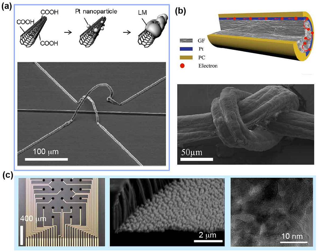
Pt nanostructures used for bioelectronics. (a) Top: A schematic diagram shows Pt nanoparticles as interface materials in the preparation of carbon nanotube/liquid metal (LM) composite. Bottom: SEM image of a 3D structure of printed Pt/CNTs/liquid metal composites. Reproduced from ref.336 with permission from the American Chemical Society, copyright 2019. (b) Top: the structure of a Pt coated graphene fiber (GF) with an as yet unrivalled charge injection capacity of ~10 mC⋅cm−2. Graphene, as current collector, improved the charge injection capacity of the system via a strong synergistic effect. Bottom: SEM image of a tied knot shows the flexibility of the graphene microfibers. Reproduced from ref.342 with permission from Wiley, copyright 2019. (c) Optical image (left), cross-section SEM image (middle), and high-resolution TEM image (right) of the porous Pt nanorods obtained from dissolution Ag from a co-sputtered PtAg alloy. Reproduced from ref.352 with permission from the American Chemical Society, copyright 2019.
PtNP-decorated silicone composites have a high surface area and can produce a cathodal charge storage capacity of ~50 mC⋅cm−2, comparable to highly doped organic electrode coatings.337 PtNPs also improve the current density and detection sensitivity of a graphene-based glutamate sensor338 and glucose sensor,339 owing to their superior catalytic behavior over hydrogen peroxide (H2O2). When combined with natural reducing agents, such as tannic acid (TA) polyphenols,340 the catalysis of H2O2 is accelerated via synergistic effects.
b). 1D Pt structures.
Pt wires or fibers have also been widely utilized as electrodes, especially for measuring extracellular activity in vivo. Alloyed with Ir, electrodes are strengthened while retaining the chemical stability and biocompatibility. Pt-Ir shows low conductor resistance (impedance of ~400 MΩ⋅μm2 at 1 kHz) but with a limited CIC below 200 μC⋅cm−2,341 which limits its usage in liquid solutions due to possible toxic products generated from Faradic interfacial charge transfers. Further improvements can come from synergistic effects with carbon. For example, a coaxial graphene/Pt fiber-like electrodes showed an increased CIC of ~ 10 mC⋅cm−2 (Fig. 12b).342
c). 2D Pt structures.
Planar Pt materials are attractive as recording sites in bioelectronic devices. With nanofabrication and photolithography, Pt of a few nanometres thickness is patterned with spatial precision on Au interconnection networks, as shown in many state-of-the-art electrophysiology probes, such as the flexible 3D mesh electronics,10, 40, 343 and neuron-like electronics344. Encapsulated by flexible polymers, these probes seamlessly integrate with biological tissues (for example, brain), which helps the signal transduction for electrophysical recording or stimulation and elicits minimal cell losses at the interface.
d). 3D Pt structures.
3D nanostructured Pt electrode arrays are widely applied as 3D metamaterials in different interfacing scenarios. For example, vertically aligned Pt nanopillars have been utilized in measuring both intracellular and extracellular activities from individual cells.345–347 Pt pillar arrays can be constructed via focused ion beam (FIB) milling and FIB-assisted Pt deposition.345 This technique, however, is incompatible on flexible substrates like parylene C. While electrochemical deposition348, 349 and dealloying Pt-based compounds350, 351 can result in 1D Pt nanostructures, noxious byproducts, such as electrochemical surfactants and Pt black, limit its usage.
3D porous Pt constructed by selective chemical etching addresses the above-mentioned challenges. Ganji et al. synthesized porous Pt nanorods (PtNRs) on parylene C substrates by dissolving Ag from a co-sputtered PtAg alloy (Fig. 12c).352 These Pt nanorods display good stability, biocompatibility, and electrochemical parameters. With similar chemical etching, nanoporous Pt meta-electrodes fabricated by Dipalo et al. were characterized with great nanoscale surface roughness, a near-infrared (NIR) light absorption, and an intimate biointerface with cardiac cells.90 These Pt meta-electrodes function like 3D antennas, and when paired with plasmonic optoacoustic poration, can record intracellularly. Overall, porous Pt meta-electrodes have several merits compared to 3D arrays with high aspect ratio Pt nanostructures, including easier fabrication, simple electronic circuitry design, and cost-efficient large scale production.
5.1.2. Au
Au is another good candidate for forming bioelectrical interfaces because of its excellent electrical conductivity, ductility, biocompatibility, chemical stability, and various fabrication and surface modification methods. Besides, Au has plasmonic properties, which can be used to generate localized heating in the vicinity upon light irradiation. Thus, Au has been widely used in many bioelectronic systems, as interconnections and leads for sensing, by enhancing tissue engineering as a good conductor, and to modulate and sense biological behaviors via plasmonic responses.
a). Au for electrical sensing.
Au nanostructures perform well in sensing intracellular action potentials in excitable cells, like neurons and cardiomyocytes. Au nanopillar with a mushroom-shaped cap can also record subthreshold synaptic activity and action potentials in vitro with minimal invasiveness for days,353 longer than the conventional patch-clamp methods. As was demonstrated by Fendyur et al., mushroom-shaped Au microelectrodes improved membrane engulfment substantially (Fig. 13a),353 which is desirable for their application due to the formation of high resistance seals between interfaced cell and the electrodes. Recently developed OpticSELINE microelectrodes354, flexible on-skin electronics,355 and aforementioned mesh electronics10 are also examples of Au-based electronics.
Figure 13.
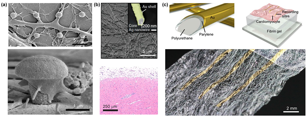
Au-based nanostructures used for bioelectronics. (a) SEM images of rat hippocampal cells cultured on Au mushroom microelectrodes. Reproduced from ref.353 under terms of the Creative Commons Attribution License from Frontiers, copyright 2011. (b) Top: SEM image and backscattered electron (BSE) image (inset) of Au–Ag nanocomposites. Bottom: haematoxylin & eosin (H&E) staining of Ag–Au nanowires implanted cardiac muscles shows little fibrotic reaction and inflammatory response. Reproduced from ref.358 with permission from Springer Nature, copyright 2018. (c) Top: A schematic diagram of the ultrasoft Au-deposited parylene–polyurethane nanomesh (left). This ultrasoft electronics can be used for mapping the electrophysiological dynamics during cardiomyocytes beating (right). Bottom: An optical image of the ultrasoft nanomesh. Reproduced from ref.362 with permission from Springer Nature, copyright 2018.
For intracellular recordings of single-unit electrical activities of networks of neurons and refined modulation of subthreshold events, Au nanopillars345, 356 and monocrystalline Au nanowires (AuNWs) of ~100 nm in diameter357 are valid. The AuNWs were grown on sapphire substrates via CVD and later mounted on a tungsten (W) tip that was coated with nail varnish solution for passivation. AuNWs are also widely applied in flexible electronics that are wearable and implantable. For example, Au-coated Ag nanocomposites (Fig. 13b) in an elastomeric block-copolymer matrix exhibit an excellent conductivity of up to ~73,000 S⋅cm−1, and a stretchability up to more than 800%.358 This Au-Ag nanocomposite conformed to human skin and swine heart, and performed electrophysiological recording and electrical/thermal modulation. The inert Au coating prevented silver oxidation and ensured biocompatibility.
b). Tissue engineering.
Cardiac patches made of 3D porous biomaterial scaffolds with seeded cardiac cells can be used to treat damaged heart tissues after a heart attack.359–361 While the porosity of polymer substrates offers environmental cues for healthy cell growth and functioning, it is expected that integration of electrically conductive materials can not only enable electrical sensing,362 but also increase synchronized contraction of cardiac cells and therefore improve the therapeutic value of the cardiac patch.363, 364 For example, ultrasoft polymer nanomeshes with 100 nm of Au deposition have been demonstrated by Lee et al. to map electrophysiological dynamics during cardiomyocyte beating (Fig. 13c).362 Besides, Au-decorated alginate cardiac patches designed by Dvir et al. enhanced electrical communication between adjacent cardiac cells and thereby improve synchronization of cell contractions.364
An on-off on-demand drug release functionality can be integrated by depositing drug-loaded electroactive polymers within Au-decorated cardiac patches. For example, negatively charged chondroitin 4-sulphate hydrogels can load positively charged growth factors and cytokines, such as insulin-like growth factor 1 (IGF-1), vascular endothelial growth factor (VEGF), and stromal cell-derived factor-1 (SDF-1), while positive polypyrrole (PPy) films can load dexamethasone (DEX). These biochemical cues control cardiac function and improve therapeutic effects of the patches through different regulation pathways.6
c). Plasmon-enabled bioelectrical sensing and modulation.
Beyond Au nanoparticle (AuNP)-based photothermal cancer therapy, plasmonic effects are also widely used for bioelectronic sensing and modulation through neural photostimulation. For example, Dipalo et al. fabricated 3D plasmonic Au nanoelectrodes for intra- and extracellular recording of spontaneous neural APs. Photo-triggered plasmonic optoporation allowed AuNWs intracellular access without perturbing ongoing electrical activity.356 Au nanorods (AuNRs), generating surface plasmons in response to near-infrared light, can facilitate neuromodulation through the optocapacitive effect.65, 66 In contrast to this, the ability to photothermally inhibit single-neural activity in vitro with NIR-sensitive nano-Au has also been reported by Yoo et al.64, 365, 366
d). Fabrication and surface modification.
A variety of approaches have been reported to fabricate nano- and microscale Au, for example the reduction of HAuCl4 into Au nanorods by citrate or borohydride367 in water solution (bottom-up method), photolithography, and electron beam lithography (top-down method). Reported by Lu et al., welding under relatively low pressures and near room temperature produced crystalline AuNW network with diameters smaller than 10 nm.368 The atomic diffusion and surface relaxation enabled cold welding within seconds merely via mechanical contact. This nanoscale welding is expected to advance bottom-up assembly of 1D metallic nanowires in future bioelectronics with improved mechanical durability and electrical properties.
Surface functionalization of Au can promote desirable functions, such as physisorption of biological cargo loading and cell adhesion, and create favourable electrostatic or ligand-receptor interactions by replicating naturally occurring binding sites. For example, ligands like Ts1 promote AuNPs binding to neuronal membrane with washout resistance.66 Arginylglycylaspartic acid (RGD), the most common motif responsible for cell adhesion to the extracellular matrix (ECM), can promote membrane/Au contact and cause the phagocytosis-like cell engulfment of the Au-mushrooms nanoelectrodes.369 Electrostatically charged polymers, such as polylysines370 and polyornithines,371 have also been widely applied to enhance cell adhesion to Au nanoelectrodes. Additionally, Au nanoelectrodes coated with Pt, iridium oxide (IrOx), and titanium nitride (TiN), offer excellent electrical coupling, surface area, and cell adhesion characteristics without influencing the plasmonic performance. Au-nanostructured microelectrodes were also used as a component in a system to process to detect cancer in unprocessed serum, in conjunction with a gene-responsive peptide nucleic acid coating and Ru(NH3)63+/Fe(CN)63− electrocatalytic redox pair372
Overall, different surface coating materials, ranging from binding motif-mimicking synthetic coatings to natural extracellular matrix gels, such as fibronectin, laminin, and collagen, and to inorganic materials, interplay with biological systems through differing mechanisms and can induce various biological responses and downstream regulations.373–375
5.1.3. Liquid Metal
Taking advantage of the extreme deformability and excellent metallic conductivity, liquid metals are widely used in many flexible bioelectronic devices or e-skins, such as Ga-based neural probes,376, all-soft matter circuits,377 and conformal and reconfigurable electronics that can undergo extreme strains.329, 378 While the most well-known liquid metal, mercury (Hg), is lethally toxic, gallium (Ga) and several Ga-based alloys, commonly gallium indium (EGaIn) and Galinstan, are considered to be biologically safe.379
In air, the surface of Ga quickly forms a thin oxide layer, which prevents surface tension-driven droplet formation and thereby allows the patterning of Ga into designed geometries and structures. The electrochemistry of native surface oxides of Galinstan in electrolyte solution is highly dependent on the electrolyte concentration. Ga oxide can be removed via etching with acidic (pH<3) or basic (pH>10) solutions or via electrochemical reactions under a reducing bias.380, 381 For example, NaOH solution dissolves Ga(III) oxide and produces NaGa(OH)4, which forms hydrophilic interfaces and results in low interfacial tension between the electrolyte and liquid metal.382
Along with an increasing number of studies focused on the liquid metal-based bioeletronics, several patterning methods have been developed to fabricate liquid metal traces, for example, microfluidic injection, additive and subtractive process, and lithography methods.383 Recently, liquid metal patterning technologies to match cellular dimensions have been developed. To achieve single cell spatial resolution, all-soft EGaIn-based devices with submicron feature sizes down to 180 nm were created.384 Fabricated using both electron-beam lithography and soft lithography, this device generated the current highest resolution of liquid metal patterning. Additionally, sonication has been used to produce liquid metal droplets for printable devices. The morphology of liquid metal particles can be stabilized by positively charged molecular or macromolecular surfactants, such as cetrimonium bromide (CTAB) and lysozyme.385 Embedded in polymers, liquid metal-based soft electronic devices are not only stretchable, but also self-healing. For example, abundant hydrogen bonds in PVA recovered the mechanical and electrical properties of patterned liquid metal circuits after cutting without any addition of any agents or solvents.386 Liquid metal-suspended soft elastomers also have self-healing abilities without requiring manual repair or external heat.387 When impaired, the metal droplets break to generate new connections with nearby metal droplets, rerouting the transportation of electrical signals without disruption. For more information about the chemistry, physical properties, patterning, and device fabrications of liquid-metal-based materials, readers may refer to available literature.329 , 388
5.1.4. Other Metals
Nano-silver structures, e.g., Ag nanowires (AgNWs), and 2D Ag flakes, have received extensive attention as conductive fillers for stretchable bioelectronics or rubbery transistors. Ag is highly conductive and mechanically durable, and AgNW-based meshes or arrays can have high conductivity due to contacts between long nanowires. Besides previously mentioned Au-Ag nanocomposites,358 other Ag nanostructures have also been embedded in stretchable polymers, such as polyurethane (PU) and polydimethylsiloxane (PDMS), to make devices that can endure ultrahigh stretching. Yang et al. seeded high density AgNWs into PU using intense pulsed light, which heated local PU so that it melted and softened to allow AgNWs to be embedded.389 Light-induced melting of PU enables tight contact without breaking the substrate, while simultaneously improving junction conductivity between each nanowire. Similarly, Kim et al. embedded AgNWs in P3HT-percolated PDMS to construct stretchable transistors,390 where AuNPs were also coated onto the AgNWs for reducing the energy barrier between the source and the drain. Recently, 2D Ag flake-based conductive networks in a fluorine rubber were studied by Matsuhisa et al. As 2D nanostructures have a larger junction area, which in turn allows for reduced contact resistance, 2D Ag flake-based conductive rubber presented a high conductivity of more than 700 S⋅cm−1 at 0% strain.391 With in situ formed AgNPs, a reinforcement effect led to a conductivity ten times higher than Ag flakes alone (about 6000 S⋅cm−1 at unstretched stage).392
Stainless steels (SS) possess good stability, resistance to corrosion, and are characterized with good electrochemical properties, for example, capacitive interfacial charge transfer. A study by Schwarz et al. using SS probes 30-50 μm in diameter successfully recorded brain activities in unrestrained, naturally moving rhesus monkeys for close to five continuous years.393 The scalability of SS also enables large-scale monitoring with volumetric probes with thousand-channel capacity. However, most stainless steels are not compatible with magnetic resonance imaging (MRI) because of their iron-rich chemical composition, which induces severe magnetic field distortions.394 Therefore, stainless steel induces undesirable artifacts and is potentially unsafe for patients under MRI testing as high frequency magnetic fields may cause high magnetic dislocation forces and torque.
Comparatively, Cu is considered MRI safe with minimal imaging artifacts within a magnetic field less than 40 T⋅m−1.395 Although Cu is acceptable to use in MRIs due to its low magnetic susceptibility, close to that of water and tissues, the potential cytotoxicity of Cu impedes its direct implantation for in vivo applications.396, 397 Zhao et al. overcame this limitation by encapsulating the Cu microelectrodes with graphene via a low-pressure CVD process. Remarkably, graphene-coated Cu (G-Cu) electrodes generate negligible magnetic field distortion and MRI artifacts, presenting great opportunities for simultaneous brain activity mapping and electrophysiological recording. Cu, a cheaper alternative to Au, is also widely used as interconnecting wires in flexible electronics in serpentine or waveform patterns that can survive extreme strains.398, 399
5.2. Carbon
Graphene and carbon nanotubes (CNTs) are favoured in bioelectronics for their outstanding chemical stability, biocompatibility, high mechanical flexibility, large surface area, a wide electrochemical window for doping and modification, and a variety of fabrication methods.400 Many flexible monolithic devices and fiber-like probes are fabricated with nanocarbon for bioelectrical sensing,401, 402 energy storage,403 and electrochemical measurements404. Furthermore, carbon microelectrodes with nanoscale tips (Fig. 14a) are ideal for high resolution measurement of synaptic activities and vesicles (Fig. 14b).405 With a carbon fiber in a cell or at close proximity to a cell, oxidation currents elicited by known redox reactions (Fig. 14c) can be electrochemically detected.405–409
Figure 14.
Carbon microfiber used for intracellular electrochemical detection. (a) SEM of an insulated carbon microelectrode with nanoscale tip. Reproduced from ref.407 with permission from the American Chemical Society, copyright 2020. (b) A schematic diagram shows single-cell intracellular measurements of vesicles and synaptic activities using a carbon-fiber microelectrode. (c) On a carbon electrode, vesicles rupture and expel contents, for example norepinephrine (i), epinephrine (ii), octopamine (iii) or dopamine (iv). The elicited oxidation currents can be electrochemically detected by the carbon microelectrode. (b) and (c) Adapted from ref.405 with permission from Springer Nature, copyright 2017.
5.2.1. Graphene
Graphene, a 2D structure of hexagonally arranged carbon that is one atom in thickness, has been widely used in bioelectronics. It has extraordinary mobility of charge carriers near 10,000 cm2⋅V−1⋅s−1 at room temperature410 and a high surface-to-volume ratio (theoretically, a specific surface area of ~2600 m2⋅g−1). Coating carbon allotropes on top of metal microelectrodes and vice versa can lead to a synergistic effect between carbon and metal constituents, forming a structure with better electrochemical performance than either individual material, for example, lower electrode impedance, improved charge injection capacity (CIC), and higher surface area. A thin-Pt-coated graphene fiber shows an unrivalled CIC of more than 10 mC∙cm−2 and an extremely low impedance at 1kHz of ~3 MΩ⋅μm2, which is two-magnitudes lower than its Pt counterpart (~ 400 MΩ⋅μm2) and smaller compared to the graphene comparisons (~ 9 to 28 MΩ⋅μm2).342 In a wearable patch for diabetes monitoring and therapy (Fig. 15a), a serpentine bilayer of Au mesh and Au-doped graphene together showed improved electrochemical activity compared to bare graphene, owing to the formation of efficient interfaces for stable charge transfer.404 The hybrid patch, consisting of several sensors and drug delivery microneedles, stably operated under various mechanical deformations (Fig. 15b).
Figure 15.
Graphene-based bioelectronics. (a) A schematic diagram of the serpentine Au mesh/graphene-based diabetes patch with sweat-control, sensing and therapy components. (b) Optical images of the compressed (top) and stretched (bottom) diabetes patches. (a) and (b) Reproduced from ref.404 with permission from Springer Nature, copyright 2016. (c) A schematic diagram shows the fabrication steps to obtain soft graphene contact lens on Parylene C. (d) Top: infrared fundus photo of a monkey eye taken during multifocal electroretinography (ERG) recording with a soft graphene contact lens (or GRACE device). Bottom: The response density plot of ERG signals in associated regions. (c) and (d) Reproduced from ref.427 under the terms of the Creative Commons Attribution License from Springer Nature, copyright 2018.
Graphene films are also attractive candidates for fabricating sensitive field effect transistors (FETs). Because the formation of unstable potentials at the tissue/metal interfaces causes large direct current (DC) offsets and drift, ultraslow neural activities are always distorted, making it challenging for metal electrodes to record ultraslow signals. Masvidal-Codina and co-workers reported graphene-based solution-gated FETs (or gSGFETs), in the form of 2D flexible epicortical and intracortical arrays which can serve as an alternative to metal electrodes for mapping ultraslow (below ~0.1 Hz) cortical brain activity that occurs in neurologic diseases..401
High-quality graphene can support primary neuron growth without other biomaterials.411 Graphene substrates were reported to enhance differentiation of neural stem cells and promote mouse hippocampal neurite sprouting and extension.412, 413 Graphene is also widely applied as an advanced coating biomaterial by exfoliation-and-transfer or direct CVD growth onto bioprobes.414, 415 Graphene-coated probes demonstrated excellent biocompatibility, and generally exhibit intimate and robust graphene/cell interfaces, which help cell maintain a viability of more than 90%.416 A scattered distribution of microglia and astrocytes was observed around the graphene-coated electrode.402, 417 The biocompatibility can be further improved by appropriate material treatments.418 For example, hydrophilization treatment using steam plasma419 and layer-by-layer deposition with poly-L-lysine420 improve the proximate contacts between graphene and cells.
3D graphene structures provide cells with spatial microenvironments and synergistic cell guidance cues. For example, 3D graphene foams synthesized by Ni-foam-templated CVD formed 3D interfaces with neurons, which increased the proliferation and growth of neural stem cells (NSC) and enhanced NSC differentiation towards neurons, compared to planar graphene films.421 These 3D graphene foams can also serve as a conductive scaffold for electrical cell stimulations, where an increased intracellular Ca2+ signal in neurons upon electrical stimulation was observed. Similarly, high density microelectrode arrays of 3D porous graphene, fabricated by direct laser pyrolysis, offer a minimally invasive but efficient cortical neuromodulation and sensing.422 As was demonstrated by Lu et al., the porous graphene can be doped with 70% nitric acid to decrease electrode impedance and increase the charge injection capacity.423
Graphene has broadband optical transparency of more than 90%, which can benefit simultaneous optical imaging, optogenetic stimulation, and electrophysiology.424–427 For example, contact lenses fabricated from graphene on soft Parylene C film (Fig. 15c) enabled simultaneous in situ infrared fundus visualization during multi-electrode electroretinography (ERG) recording (Fig. 15d).427 Transparent graphene contact lenses have also been applied for electromagnetic interference shielding,428 glucose level measurement,429 and intraocular pressure sensing.430 Besides, Kuzum et al. have demonstrated transparent flexible 2D graphene neural electrodes that provide simultaneous neural calcium and electrical visualization with high spatiotemporal resolution.424 However, a few layers of graphene generate photoelectrochemical currents during light illumination, which may interfere with the neural electrophysiological signals and produce artifacts.431
Graphene is magnetically insusceptible, and therefore ensures a negligible artifact during magnetic resonance imaging (MRI). Zhao et al. fabricated a graphene-covered copper (G-Cu) microwire that is compatible with 7.0 T MRI scans as well as being biocompatible and nontoxic.402 A thin layer of graphene prevents Cu-induced acute tissue toxicity and fast corrosion of Cu. However, over chronic implantation, the rigidity of the G-Cu microelectrodes may elicit neuroinflammation, such as activation of microglia and astrocytes and glial scar formation.
5.2.2. Carbon nanotubes (CNTs)
Similar to graphene, CNTs show a capability to reinforce cell adhesion and growth.432–434 The large surface area of CNTs promotes neuron adhesion and the formation of tight junctions between CNTs and neural cell membranes, facilitating sensitive recording or efficient electrical stimulation. Excellent biocompatibility of carbon-based nanomaterials can be achieved by adjusting the dosage, surface chemistry, and structure patterning into various architectures that are ideal for biointerfaces.
CNTs display electrical conductivity ranging from metallic to semiconductors, depending on the orientation in which the carbon is wrapped. The specific impedance of CNT fibers is ~20 mΩ⋅μm2, which is only one-twentieth of Pt/Ir (~400 mΩ⋅μm2), while the charge injection limit of CNT fibers is ~6 mC⋅cm−2, sixtyfold larger than Pt/Ir (~100 μC⋅cm−2) with the same geometrical area.435 The low impedance and the large CIC enable a remarkably high SNR and charge injection across the bioelectronics/cell interfaces.
The flexibility of CNTs allows for conformal integration on human body and within dynamic tissue environments, and CNTs have been broadly examined in many intrinsically stretchable transistor-based bioelectronics436, 437, self-healable electronic skins,438, 439 and implantable microfibers.16, 440 By varying the size and hierarchical structures of CNT, tissue-comparable bending stiffness of ~10−8 nN⋅m2 can be reached in a case of carbon helical fiber bundles (Fig. 16a and b),16 which is much lower than those of Si wires and Au wires (~ 0.1 nN⋅m2). This flexibility allows for conformal integration within dynamic tissue environments and helps to reduce inflammatory responses (Fig. 16c). Similarly, a soft ultra-small MRI compatible implant based on CNTs formed a scar-free neural interface, allowing for stable recording of single-unit action potentials for several months. With magnetic insusceptibility, MRI global mapping of brain activity can be performed during electrical recording.440
Figure 16.
Hierarchical carbon fiber-based bioelectronics. (a) A schematic diagram shows the hierarchical helical bundles of muscle. (b) Top: TEM image of a multi-walled CNT, the building block for a CNT-based hierarchical helical bundle. Middle: SEM image of a primary CNT-based fibre. Bottom: SEM image of assembled hierarchical helical CNT bundles. (c) Left: a schematic diagram shows the CNT helical fibre bundles can be injected into blood vessel for in vivo monitoring. Right: photograph of the skin surface of a cat after injection with a CNT-based multiply sensing fibre. (a) − (c) Reproduced from ref.16 with permission from Springer Nature, copyright 2019.
5.3. Oxides, nitrides and carbides
The use of graphene oxide nanosheets (s-GO) to selectively downregulate the glutamatergic synaptic activity of hippocampal neurons in vitro and in vivo was reported by Rauti et al., who exploited the use of carbon for trimming down specific synaptic activity and target joint diagnostic/therapeutic applications.441 Reduced graphene oxide (r-GO) has also been reported with enhanced charge injection capacity that is preferable for electrical neural stimulation.442 These graphene oxides can be reliably prepared via modified Hummers methods, where potassium permanganate is added into a solution of graphite, sodium nitrate, and sulfuric acid.443, 444
Metal oxides with nanostructured surfaces, such as iridium oxide (IrOx) nanotubes, can interrogate cultured cells. For example, Cui et al. have demonstrated the usage of IrOx nanotube electrodes for intracellular action potential detection.445 This platform was used to evaluate the effect of ion-channel blocking drugs on the electrophysiology of cardiomyocytes with significantly improved SNR. These hollow nanotube arrays would be more valuable than solid nanowires when there is a need for intracellular sampling or intracellular delivery of materials such as drugs.
Oxides and nitrides, such as ZnO nanowires, titanium nitride (TiN), and IrOx have also been used as coating materials to improve the electrode performance. Coated with TiN, Pt-Ir electrodes can be largely improved to reach a 5-fold increase in CIC, due to the large effective surface area TiN provides. The roughness of TiN surfaces also promotes cell adhesion in many cases, for example, the TiN-coated Au cardiac patch.6 When coated with IrOx, Pt-Ir reaches a higher charge capacity of around ~5 mC⋅cm−2 because of the charges transferring in a reversible faradaic reaction between Ir3+ and Ir4+ oxide states.
MXenes, which are a class of 2D transition metal carbides, nitrides, or carbonitrides, have been used mostly for energy storage applications. They have tuneable surface terminations, high conductivity, and remarkably high volumetric capacitance.446 Recently, Driscoll et al. used 2D Ti3C2 MXene as high-resolution neural electrodes.447 Distinct among carbon-based nanomaterials, Ti3C2 is processable in aqueous dispersions. Possessing high effective surface area, this MXene-based neural interfaces displayed low impedance, good sensitivity for neural signals, and high spatiotemporal resolution. Besides serving as biocompatible electrodes, the MXene family of materials may also yield high power density energy storage systems for bioelectronics.
6. Organic conductor-based bioelectronics
The synthesis of conducting materials that are highly flexible while maintaining mechanical integrity remains one of the most challenging aspects facing bioelectronics to date. Organic conducting materials, including conjugated polymers and hydrogels, can be more biocompatible and easier to fabricate compared to most inorganic materials.448 For hydrogels, in particular, their Young's moduli and water content are much closer to those of biological tissues, allowing them to form more compliant biointerfaces while at the same time, providing satisfactory electrical performance via ionic conduction.71, 449 While many conductive polymers have been identified for applications in flexible electronics,450 only a few have been used for bioelectronics. Current research focuses almost entirely on three in particular: Poly(3,4-ethylenedioxythiophene):poly(styrene sulfonate) (PEDOT:PSS), polypyrrole (PPy), and polyaniline (PANI).289, 451 The characteristics of these polymers are summarized in Table 3.
Table 3.
Characteristics of common organic conductors used for bioelectronics.
| PEDOT:PSS | PPy | PANI | |
|---|---|---|---|
| Systematic name | Poly(3,4-ethylenedioxythiophene):poly(styrene sulfonate) | Polypyrrole | Polyanilline |
| Chemical structure* | 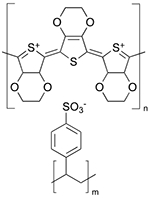 |
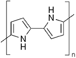 |
|
| Characteristics | - The most studied conductive polymer - Mixture of two ionomers - Poor mechanical stability, requires fixing or composite formulation |
- pH-sensitive conductivity - Mechanoelectric properties - Can be synthesized through photopolymerization |
- Low-cost precursor and synthesis - pH-sensitive conductivity - Can be synthesized in situ onto biological structures |
The exact structure depends on protonation and oxidation states and will vary depending on the conditions.
6.1. PEDOT:PSS
Poly(3,4-ethylenedioxythiophene):poly(styrene sulfonate), or PEDOT:PSS, is a polymer mixture formed of two ionomers that has proven to be one of the most promising conductive polymers for bioelectronics. PEDOT synthesized through oxidative polymerization is conductive but insoluble in water. A counterion, PSS, is added to increase its dispersion and stability via Coulomb interactions therefore making it suitable for the synthesis of hydrogels.452 PSS is an insulator, and the conductivity of the overall composite is determined by the PEDOT crystallinity. This combination offers numerous advantages in terms of processability and biocompatibility. Whereas conventional hydrogels are generally poorly conductive, PEDOT:PSS hydrogels possess a highly tuneable electron and ion conductivity using a variety of dopants, which either add or remove π-electrons from the polymer matrix.453, 454
6.1.1. Chemistry-enabled conductivity, stretchability, and adhesion
One of the challenges in PEDOT:PSS chemistry is managing the strong π-π interactions that are necessary to achieve conductivity. Most PEDOT:PSS materials are prepared as composites, with additives such as poly(vinyl alcohol),455 acrylamide,456 and polyacrylic acid457 allowing for the formation of hydrophobic fibers to minimize unfavourable interactions in their structure. Yeon et al. found that blending dodecyl sulfate to PEDOT:PSS aqueous solution enhances the conductivity by selectively removing insulating PSS, increasing interconnectivity between conductive PEDOT cores.458 This technique allowed them to achieve high conductance materials that can be blended with fabrics and used as Joule heaters for thermal stimulation. However, such additives could potentially compromise the electrical properties of the polymer, so an alternative approach is to fabricate PEDOT:PSS as a thin film and then transfer and fix it onto other elastic substrates, e.g., PDMS. This preserves the high conductivity of native PDMS, while also providing the additional mechanical stability offered by the presence of the substrate. Numerous transfer printing methods have recently been reported that could enable high-throughput synthesis of such devices.459–462
An important merit of organic bioelectronic devices is their ability to withstand mechanical stress and maintain their useful properties under deformation. While PEDOT:PSS can only sustain near 2% stretching, modification using dopants and copolymerization permits high composite flexibility. For example, Cuttaz et al. demonstrated that the combination of PU and PEDOT:PSS formed a conductive elastomer that integrated the flexibility of PU and the conductive properties of PEDOT:PSS.463 It was shown that these materials could be directly laser micromachined into devices with comparable performance to Pt arrays in in vitro experiments. Additionally, the conductive properties of PEDOT:PSS can stimulate and promote tissue regeneration. In recent work, Iandolo et al. demonstrated 3D printed scaffold made of conductive polymer-based composites that support bone regeneration and showed the proof of concept using human fetal mesenchymal stem cells.464
Most dopants are capable of improving either mechanical or electrical properties, but not both. To resolve this issue, Wang et al. proposed the application of additives called stretchability and electrical conductivity (STEC) enhancers, taking inspiration from a styrene-ethylene-butylene-styrene block copolymer elastomer structure.465 The authors suggested that properly chosen STEC enhancers can weaken the PSS interaction with PEDOT, softening PSS domains while promoting high conductivity and crystallinity in the PEDOT network (Fig. 17a). This architecture yields a stretchable and conductive PEDOT:PSS-based material. They identified numerous potential STEC enhancers such as sodium dodecyl benzenesulfonate, dioctyl sulfosuccinate sodium salt, and bis(trifluoromethane) sulfonamide lithium salt. The PEDOT:PSS films thus obtained achieve conductivities up to 4100 S⋅cm−1 under 100% strain. They validated the utility of the material by fabricating interconnects for electrical devices that preserve the conductivity under mechanical stretch and large deformations (Fig. 17b). In another example, D-sorbitol was used as both a secondary dopant and plasticizer to improve biocompatibility and to permit conductivities higher than 1000 S⋅cm−1 under strains greater than 60%.466 d-sorbitol can form hydrogen bonds with the hydroxyl groups of polymers such as PEDOT:PSS, promoting phase segregation and increasing the overall stretchability of the material, as well as inducing conformational changes for the formation of conductive PEDOT chains. Overall, research focusing on the stretchability of PEDOT:PSS has focused on partially reducing connections within the PEDOT:PSS matrix while either maintaining maximum PEDOT core interaction or substituting ionic additives to make up for reduced intrinsic PEDOT conductivity.
Figure 17.
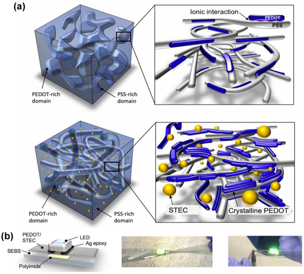
STEC-enabled PEDOT:PSS bioelectronics. (a) Schematic representations of PEDOT:PSS domains in a pristine polymer (top) and with an addition (bottom) of stretchability and electrical conductivity enhancer. (b) Left: schematic representation of LED device with interconnects made of PEDOT/STEC. Middle: photograph shows high LED brightness when the device is stretched and twisted. Right: photograph shows high LED brightness when the device is poked with a sharp object. (a) and (b) Reproduced from ref.465 with permission from the American Association for the Advancement of Science, copyright 2017.
Since additives can impair material homogeneity and invite possible cytotoxicity, synthetic strategies to increase the purity of PEDOT:PSS are desirable. Synthesis of pure PEDOT:PSS hydrogels under regular conditions is challenging due to the collapse of the fibrillar structure, which decreases the conductivity (Fig. 18a). Lu et al. have developed a method to synthesize pure PEDOT:PSS while retaining its stability, elasticity, and conductivity.467 They were able to form interconnected and pure PEDOT:PSS nanofibrils by the addition of DMSO to aqueous PEDOT:PSS, dry annealing, and rehydrating. During this process, drying the solution concentrated the PEDOT:PSS and annealing at high temperatures induced recrystallization and chain rearrangement (Fig. 18b). This results in a dry, phase-separated system that, when maintained in a well-spaced network, remains interconnected once the hydrophilic PSS domains are rehydrated. The mechanical properties of these gels can be tuned by varying the amount of DMSO and method of dry annealing (Fig 18c). Importantly, this technique is compatible with inkjet printing and allows for fast pattern fabrication (Fig. 18d).
Figure 18.
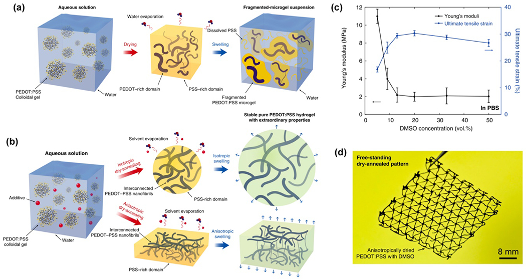
Pure PEDOT:PSS hydrogel and freestanding structure. (a) Schematic representation of PEDOT:PSS domains aggregation during water evaporation. (b) Schematic representation of fibril domain morphology in PEDOT:PSS hydrogel dried with DMSO as an additive. (c) DMSO dependent Young’s moduli and ultimate tensile strains in the pure PEDOT:PSS gels. (d) Free-standing PEDOT:PSS pattern fabricated using inkjet printing. (a) − (d) Reproduced from ref.467 under the terms of the Creative Commons Attribution License from Springer Nature, copyright 2019.
Finally, to enable adhesive properties, a mussel-inspired PEDOT:PSS composite was recently synthesized by Gan et al. by using PEDOT:PSS and polydopamine-reduced sulfonated graphene oxide (PSGO). The material was highly elastic, redox-active, and strongly adhesive due to the abundance of catechol groups that can effectively interact with a range of substrates. Its utilities in bioelectronic applications was demonstrated by recording a range of bioelectrical signals using both epidermal and implantable electrodes.468
6.1.2. Chemistry-enabled functionalities in electrochemical transistors
Ion-gated organic electrochemical transistors (IGTs) are promising in bioelectronics, however most IGTs operate only in depletion mode (are conductive under zero bias) and are not suitable for sensitive recordings. Fabrication of enhancement mode IGTs (e-IGTs) requires nontrivial chemical modifications, which often make the device hydrophobic, unstable or cytotoxic, therefore compromising its biocompatibility. To address these challenges, Cea et al. devised a composite of PEDOT:PSS with polyethylenimine (PEI) to realize a biocompatible e-IGT.469 Main components of the active channel in the new e-IGT are PEDOT:PSS, PEI and ᴅ-sorbitol. ᴅ-sorbitol was used as a biocompatible stabilizer to increase hydration and mobility of ions, but novel electrical properties come from the interaction between PEDOT:PSS and PEI (Fig. 19a). PEI causes electron transfer and reduction of PEDOT through formation of PEI:PSS complexes and causes de-doping in PEDOT which loses its conductivity. Upon application of gate bias, PEI gets protonated and releases PSS, which upon binding with PEDOT, restores conductivity in the channel. The resulting material is highly stable and the redox reaction ideally reversible.
Figure 19.
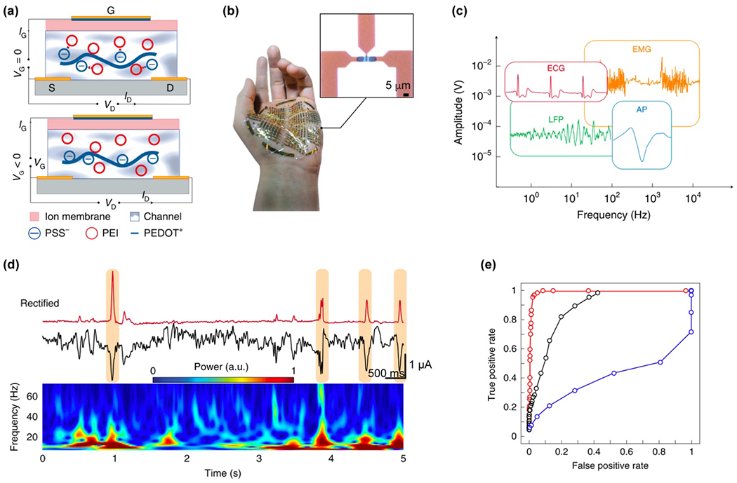
e-IGT for bioelectronics. (a) Schematic illustration of e-IGT device operation. Protonation of PEI+ under negative gate potential releases PSS- which upon binding to PEDOT reinstitutes its conductivity. (b) Photograph showing conformance of the ultra-thin e-IGT based device to the human hand. Inset shows the microphotograph of an individual junction. (c) Traces of sample signals recorded with e-IGT-based devices spanning through amplitude and frequency ranges. (d) Output of nonlinear rectifier made of IGT-based circuit. Top: marked spikes show epileptic discharges. Bottom: Power spectrogram of the recording. (e) Operating curves showing improved detection performance of nonlinear amplifier (red) over bandpass filter (black) and amplitude (blue) thresholding. (a) – (e) Reproduced from ref.469 with permission from Springer Nature, copyright 2020.
The obtained materials can be easily fabricated using a standard lithographic approach to form thin and flexible membranes (Fig. 19b). The applicability of e-IGTs was validated by recording a number of different bioelectronic signals (Fig. 19c). To demonstrate long-time in vivo biocompatibility, soft circuits made of depletion and enhancement IGTs were used for nonlinear signal amplification of high-fidelity detection of epileptic discharges (Fig. 19d). Such local nonlinear amplifiers showed both a high response rate as well as improved detection quality over classic thresholding methods (Fig. 19e). The devices were stable for over two weeks after implantation and provided high quality recording from freely moving animals. This study is an excellent example of how chemical principles can be applied to realize new functionalities while at the same time preserving the stability and biocompatibility of the device.
6.2. PPy
Polypyrroles (PPy) offer similar advantages as PEDOT:PSS for conductive, organic bioelectronics. When oxidized, PPy becomes conductive because of delocalized π-electrons in a conjugated double bond network along the polymeric nanofibrils. Furthermore, they are highly biocompatible and environmentally stable. Ease of synthesis, thermal stability, and biocompatibility make this material uniquely useful for bioelectronic applications. PPy is typically synthesized as monolithic sheets that are highly conductive and accrue significant actuation strain after the application of an electric current. Therefore, PPy can also be used for electrochemically induced strains in the fabrication of artificial muscles or mechanomodulation.470 Additionally, PPy can be synthesized through photopolymerization, and free-standing structures can be fabricated using methods of 3D additive manufacturing471 and two-photon polymerization.472 One of the drawbacks is the high sensitivity of PPy to the pH of the environment and the strong correlation between protonation level and conductivity. In order to address these difficulties, different PPy microstructures were evaluated, and it was found that conductivities of nanotubular structures were up to ten times stronger than for globular PPy, even in body pH levels.473, 474
6.2.1. Chemistry-enabled adhesion
PPy films are intrinsically stretchable but do not easily adhere to cells and tissues. Texidó et al. found that doping PPy with hyaluronic acid strengthens the composite’s adhesion to stretchable materials such as PDMS, offering an alternative means to create stretchable PPy-based conductive devices.475 Another report shows strong dependence of hyaluronic acid molecular weight on its adhesive properties with higher molecular weight providing improved adhesion, higher electrochemical activity and lower impendence of the bioelectrodes.476 A dopant-free solution for achieving strong adhesion is direct PPy polymerization on a porous PDMS surface that has been pre-activated using UV/ozone oxidation. With this technique, Tsao et al. built stretchable devices on three-dimensional PDMS substrates that have high stretchability and stable conductivity, and which can be used for measuring stretching forces.477
One issue that consistently arises is that conductive polymers generally become hydrophobic once optimized for their conductive, optical, and elastic capabilities. For bioelectronics, it is important that a material be self-adhesive and interface well with a biological tissue. Recent research has focused on the synthesis of PPy composites, incorporating additives to improve its hydrophilicity. Han et al. found that incorporating polydopamine (PDA) via in situ formation of PDA-PPy nanofibrils (Fig. 20a) within a polyacrylamide matrix increases its overall hydrophilicity while retaining transparency and its electronic properties.478 They found that functional groups on PDA bond with water molecules while its catechol groups form a complex with PPy, creating an electrically functional (Fig 20b), hydrophilic composite device capable of transmitting 70% of the visible spectrum (Fig. 20c and d). The material can withstand strains exceeding 2000% and adheres with ease to the human skin tissue, which was demonstrated by the fabrication of electrodes for MCG and ECG. Beyond copolymerization, deposition of adhesive biomolecules has shown promise for increasing PPy adhesion. Jang et al. demonstrated a method to immobilize Arg-Gly-Asp peptide on the electrode surface using electrodeposition.479 By varying electrodeposition time, they achieved high control over peptide surface density without significantly affecting the electrical impedance of the electrode. Material adhesion properties were quantified using in vitro biointerfaces with human mesenchymal stem cells.
Figure 20.
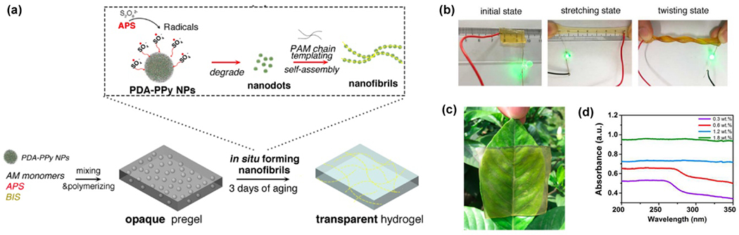
PDA-PPy hydrogels. (a) Schematic representation of in situ transformation of PDA-PPy nanoparticles into transparent fibrils. (b) Demonstration of the electrical conductivity of the hydrogel (6 wt. %) under stretching and twisting. (c) Photography of transparent hydrogel on a leaf. (d) UV-vis absorption spectra of hydrogels prepared with different PDA-PPy concentration. (a) – (d) Reproduced from ref.478 with permission from the American Chemical Society, copyright 2018.
To accurately sense or stimulate a desired target molecule or cell, the device must be able to integrate with that target specifically. This issue led to the development of methods for targeted adhesion. One method for obtaining targeted adhesion can be the integration of antibodies or biomolecules with the materials. Golabi et al. used 4-N-Pentylphenoboronic acid as a functional dopant with PPy to specifically increase its affinity towards diols.480 Boronic acid interacts with cis-diol to form cyclic esters and interfaces well with PPy, thus making it an ideal candidate to create PPy devices that selectively interact with organisms with sugar-rich membranes like bacteria. Golabi et al. further researched PPy bacterial differentiation using a variety of ion dopants. They found that adhesion of specific bacterial strains can be modulated by changing the dopant type.481 This material allowed the creation of a new method of label-free bacterial differentiation. Further studies will focus on electrical modulation or stimulation for bacterial adhesion, which might prove useful for monitoring of bacterial population in mixed culture. This, in turn, could be used in a clinical setting, e.g., for monitoring the gut biome.
6.2.2. Chemistry-enabled dynamic substrates
Electroactive properties of PPy were recently used to study mechanotransduction at the nano-biointerface in mesenchymal stem cells. The Jiang group used template-free electropolymerization to obtain PPy nanotubes array on a titanium substrate (Fig. 21a).482 In this material, during the electrochemical reduction/oxidation cycle, the morphology of the interface switches between nanotubes and nanotips (Fig. 21b).482 This morphological change allowed them to cycle the interface between the highly adhesive hydrophobic surface and poorly adhesive hydrophilic surface, providing attachment and detachment stimuli to MSCs. The stimulation effectively changed the distribution of actin filaments (Fig. 21c), cell surface area (Fig. 21d), and caused nuclear translocation (Fig. 21e). Such geometric stimulation may be used in the future for smart materials promoting tissue regeneration.
Figure 21.
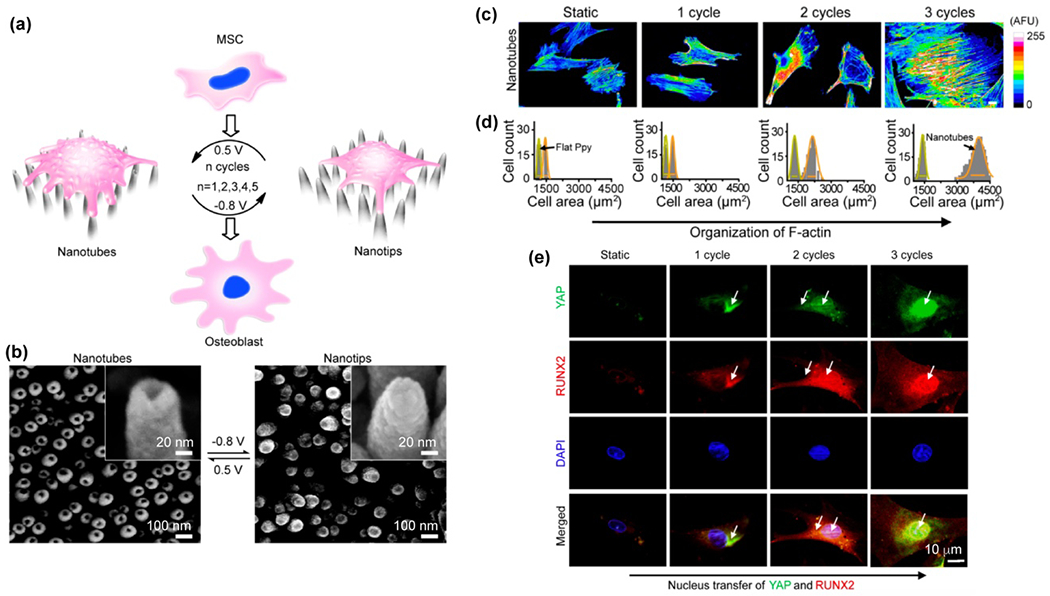
Structured PPy for mechanotransduction. (a) Schematic representation of structure switching in PPy array directing development of Mesenchymal stem cells. (b) SEM images of PPy array at the two redox states showing nanotube and nanotip geometry. Mechanotransduction effects on (c) distribution of actin filaments (pseudocoloured heat maps, scale bar 10 um), (d) cell area, and (e) nuclear translocation. (a) – (e) Reproduced from ref.482 with permission from the American Chemical Society, copyright 2017.
Electrostimulation with PPy-based conductive hydrogels was also recently used to treat spinal cord injury. Zhou et al. were able to cross-link PPy with tannic acid (TA), a plant-derived polyphenol commonly used in many medical products due to its antioxidant, antibacterial, and anti-inflammatory properties.483 Optimization of TA content allowed the authors to obtain a hydrogel with low Young's modulus and conductivity matching that of the native spinal cord. In vitro studies showed that the hydrogel stimulates differentiation of neural stem cells, while at the same time suppressing the development of astrocytes. In vivo studies in mice models of spinal cord injury showed that hydrogel implantation promotes tissue regeneration and leads to significant recovery of neural connectivity. PPy films were also successfully used for controlled drug delivery. PPy films were successfully loaded with dexamethasone484 and salicylate485 and used for electrically controlled delivery. In an interesting study, Antensteiner et al. developed a method of fabricating PPy conductive microcups through PLGA microsphere templating.486 These cups possess a unique morphology and could possibly be used for electrical stimulation, drug release, and mechanomodulation.
6.3. PANI
Polyaniline (PANI) is another conductive polymer that has been extensively studied for its applications to bioelectronics. PANI is a low-cost, easily synthesized alternative to other conductive polymers with comparable mechanical stability and electrical properties. Early reports indicated poor biocompatibility with PANI but further investigation shown that this arose from the presence of residual monomers and acid catalysts.487 Studies using optimized synthetic protocols have shown that pristine aniline, especially in a base form, is biocompatible and free of embryotoxicity.488 Similar to other conductive polymers, PANI can be produced as a freestanding film, or as composites doped with secondary materials.
6.3.1. Chemistry for material processing
Compared with other conductive polymers, PANI has some limitations towards its use in bioelectronics, namely low solubility in many solvents and reduced conductivity in higher pH environments. Crystalline nanocellulose (CNC) can be used for PANI stabilization as its surface is rich in the hydroxyl groups, which stabilize the polymer structure. Razalli et al. showed that a polyaniline-crystalline nanocellulose (PANI-CNC) composite protonates in neutral environments, which allows it to be conductive in nearly neutral pH environments typically found in biological systems.489 CNC is also an appealing material for biointerfaces due to its natural availability, biodegradability and biocompatibility, which are discussed further in Section 7.5.490 Another example of a biocompatible dopant is gelatin methacrylate. It is especially attractive for developing transient biointerfaces as it maintains a stable structure for about 4 weeks and completely degrades in about 6-8 weeks in cell culture media.491 Recently gelatin-PANI nanofibers co-doped with camphorosulfonic acid were fabricated by electrospinning and used to stimulate and direct the growth of C2C12 myoblast cells. A combination of electrical and mechanical cues for directing cell growth might prove useful for applications in tissue regeneration.
6.3.2. Chemical stabilization
Maintaining the electric integrity of conductive polymers over time is critical for the use in implant fabrication. In cell cultures, PANI has a tendency to lose dopants in a process called de-doping. Furthermore, if composites are washed off and polymer exposed to body fluids, the pH is sufficient to deprotonate amine groups of PANI, which will significantly impair its conductive properties. Preventing this unwanted alteration has been the focus of recent research. For example, Mawad et al. created degradation resistant PANI by immobilizing phytic acid, the dopant, using a prefabricated chitosan film.492 Phytic acid is anionic and interacts with the positively charged amine groups of both chitosan and PANI and thus is immobilized via coulombic interaction. This material was used to create a suture-less conductive patch that survived in vivo for two weeks. This phytic acid doped PANI/chitosan material was later utilized to develop a bioelectronic patch which can couple with a damaged cardiac tissue. The patch alters heart electrophysiology, enhancing conduction velocity across damaged cardiac walls with minimal invasiveness and only mild inflammation. 493
6.3.3. Genetically assisted chemical assembly
Presently, even cutting-edge chemical tools do not allow for the fabrication of structures that can match the structural complexity of biological systems, and there is no implantation strategy that can lead to precise placement and integration of bioelectronics. To address these challenges, new routes to self-assembled bioelectronics have to be devised. Recently, Liu et al. developed a method of selective in situ modification of cell membranes with conductive polymers guided by the expression of a catalytic enzyme.494 Classically, PANI is synthesized under oxidative and strongly acidic conditions. To create biocompatible reaction conditions, target cells were transduced with humanized ascorbate peroxidase Apex2 using adeno-associated virus vectors (Fig. 22a). Additionally, to further lower polymerization potential a mixture of monomer and dimer of aniline in 1:1 molar ratio was used as a substrate for directed polymerization (Fig. 22b). It was shown that this strategy allows for selective and efficient modification of neuronal membranes in vitro. Besides, subsequent doping of PANI with p-toluenesulfonic acid can significantly increase the conductivity of polymer structures. Also, the enzymatic system allows for synthesis of other polymers such as conductive PEDOT and insulating poly(1,1’-diaminobenzidine) (PDAB).
Figure 22.
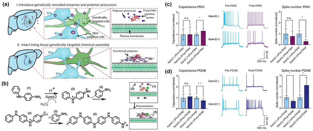
Genetically targeted chemical assembly of polymers. (a) A schematic diagram shows specific synthesis of functional polymer on membranes of genetically modified neurons. (b) Scheme of Apex2-catalyzed polymerization reaction initiated by oxidation of aniline dimer. Chemical species participating in a reaction are as follows: (1) aniline dimer, (2) aniline dimer radical cations, (3) aniline monomer, (4) aniline trimer radical cations, and (5) polyaniline (PANI). Patch clamp measurements of membrane capacitance and current potential spikes from neurons show that modification with conductive PANI increases transmembrane capacitance and decreases spike number (c) while modification with insulating poly(3,3’-diaminobenzidine) (PDAB) inversely reduces the capacitance and increases spike number. (a) – (d) Reproduced from ref.494 with permission from the American Association for the Advancement of Science, copyright 2020.
Patch clamp experiments have allowed for a thorough characterization of electrophysiology during polymer modification. It was shown that modification of neurons with conductive PANI increased their membrane capacitance and decreased spike number (Fig. 22c), while modification with insulating PDAB had the opposite effect (Fig. 22d). This method was proven successful when applied to cultured brain-slices and freely moving animals. In the former case, either excitatory or inhibitory motor neurons of Caenorhabditis elegans were genetically modified with Apex2 protein and PANI was selectively deposited. This procedure resulted in alteration of motor functions of an animal consistent with previous studies using optogenetics.495 Although the present work leaves the open questions of cytotoxicity of monomers and side products of radical oxidation reactions, it represents an important direction in the field of organic conductors. The presented methodology is especially important as similar in situ synthesis and directed self-assembly methods are likely to be developed for the inorganic materials.
7. Outlook – New Chemistry Aspects in Bioelectronics
The study of bioelectronics is, by its nature, highly interdisciplinary in that it draws from most areas of the physical and life sciences. In this section, we provide a small sample of new developments in chemistry that are of interest to bioelectronics. While each of these topics is a large and active area of research in its own right, we have selected a number of key topics that are particularly relevant.
7.1. Mechano-biochemistry
A major component of how an organism biologically adapts to its environment comes from the mechanical interactions between the two.496–498 As such, the field of mechanobiology shares some overlap with bioelectrical investigation, as both fields require an understanding of how physical stimuli can be translated into biochemical signals and vice versa. While the explicit study of coupling between bioelectricity, biomechanics, and biochemistry remains relatively uncommon,499 a number of highly relevant questions arise from considering the intersection of these fields. Here, we will examine the salient cell level processes where bioelectronics may be employed. This includes both mechanosensing as well as the processes by which cells generate and distribute mechanical forces (Fig. 23).
Figure 23.
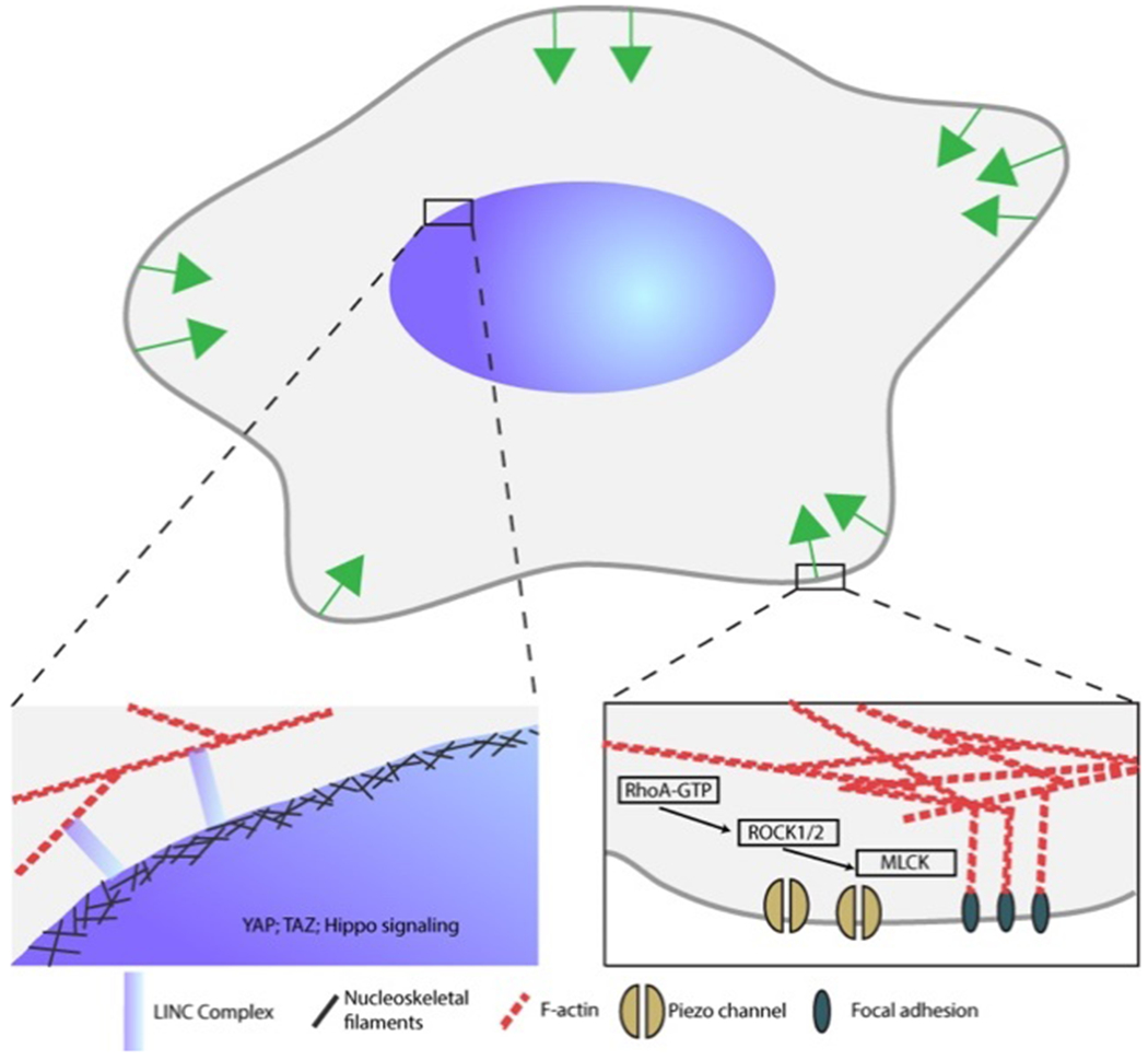
A minimal mechanical model of a cell. Top: schematic of an entire mammalian cell, with the nucleus shown in blue and the cytosol in grey. Green arrows indicate locations, orientations, and relative magnitudes of traction stresses. Lower left: mechanical components around the cell nucleus. The actin cytoskeleton is linked to the nucleoskeleton through the LINC complex. Within the nucleus, YAP/TAZ are effectors of Hippo signaling, which ultimately governs cell spreading and proliferation. Lower right: mechanical components at the cell edge. Traction stresses are transmitted from the cytoskeleton to the substrate through focal adhesions. The RhoA pathway is especially active at focal adhesions and modulates cell contractility by affecting the activity of myosin light chain kinase, MLCK. Piezo channels are both mechanically and electrically active, and therefore are integral parts of electromechanical coupling.
Cells employ a variety of methods for sensing the mechanical characteristics of their physical environments. This allows them to perform such functions as sensing the stiffness of their substrate,500 responding to stretching501 and shear flow,502, 503 and detecting local topography,115, 504 among others. Cells are also out of thermodynamic equilibrium by definition, and they actively move, change shape, and transmit forces to their local environments. A vast array of interlinked biochemical pathways function to transduce mechanical stimuli to chemical signals and back again to mechanical outputs. Within this set of pathways, we can construct a minimal mechanical model of a cell using a number of candidates that emerge as ideal targets for integration with bioelectronics.
We begin with the calcium ion, Ca2+, for a number of reasons. First, Ca2+ is a ubiquitous and well-studied secondary messenger, i.e., calcium signaling is integrated into a vast array of biological functions. This is true of mechanical functions where, depending on cell type, calcium can induce cell contractions, modulate membrane waves,505 and coordinate cell migration during development.506, 507 Second, biocompatible Ca2+ sensitive dyes are readily commercially available, so that monitoring of intracellular Ca2+ concentration is fairly easy. Finally, it is an appealing target for bioelectronic devices, as many excitable and non-excitable cell types possess voltage-gated calcium channels, such that devices may alter calcium signaling directly, through membrane potential modulation, or through alternate means, such as the optocapacitive mechanism.65
The actomyosin cytoskeleton constitutes the unifying machinery for cell mechanics. The globular protein actin assembles into long filaments (F-actin) that provide the basic structural integrity of the cell (Fig. 23). Forces are generated both from the ATP-driven polymerization and depolymerization of F-actin508 and by myosin, a molecular motor protein that forms contractile units with F-actin. Recent work has tracked the diffusivity of single charged particles, and from those results highlighted an aspect of the cytoskeleton in producing heterogeneities of intracellular mechanical and electrical characteristics.44 These results also point to the possibility of perturbing cytoskeletal architecture using electric fields alone. This may be achieved by manipulating actin509, 510 or other cytoskeletal filaments.511, 512 Another possibility is to alter molecular motor transport through bioelectronic means. To do so, we must consider where pathways involved in bioelectrical signal transduction intersect with mechanotransduction pathways.
Two of the best-studied regulators of cell mechanics are RhoA and YAP/TAZ (Fig. 23). RhoA, a small GTPase, regulates cell contractility by acting on the rho kinases ROCK1 and ROCK2, which phosphorylate myosin light chains and thereby induce contractions. Stresses are transmitted from the cytoskeleton to the substrate at focal adhesion complexes, where RhoA and ROCK activity is enriched.513, 514 Yes-associated protein (YAP) and transcriptional coactivator with PDZ-binding motif (TAZ) respond to mechanical cues – high cell density,515 low cytoskeletal stress,516 or substrate stiffness516 – by translocating from the nucleus to the cytoplasm. YAP/TAZ are effectors of the Hippo signaling pathway,517 and when present in the nucleus they encourage cell spreading and proliferation.518 The Linker of Nucleoskeleton and Cytoskeleton (LINC) complex couples the cytoskeleton to the nucleus and thus enables mechanotransduction.519, 520 These core regulators of cell mechanics intersect with bioelectronics through calcium. Like RhoA, Ca2+ is upstream of myosin light chain kinase521 and other regulators of contractility,522 and calcium is necessary to stabilize cell-cell adherens junctions, so Ca2+ dynamics can influence how cells sense their environments. There also exists a wide variety of other pathways that putatively transduce electric fields into a number of mechanical and morphological outputs, including wound healing,523 angiogenesis,524 and cell motion directionality.525
The Piezo channels are of particular relevance to bioelectronic and biomechanical applications. Piezo proteins function as stretch-activated pores of ion channels, allowing ion flux when their associated bilayer is under tension.526, 527 They are evolutionarily conserved528 and broadly important to physiology: they are necessary components in vascular development in mice,529 stem cell differentiation,530 and mechanotransduction in light touch sensing.531 Interestingly, Piezo channels also display a voltage-sensitive functionality that is also well-conserved.528 Positive applied voltages increase the probability of a channel being open, and they also allow the channel to retain sensitivity after several mechanical impulses.528 As such, Piezo channels are appealing targets in bioelectronics, both as potential targets for modulation, and as major components of electromechanically coupled machinery in cells.
Nano-biointerfaces can perturb the mechano-biochemistry just described through a number of ways. One potential route to modulation is the material properties of the bioelectronic devices, such as stiffness532–534 or topography.115, 504, 535 Exogenous impulses are also viable candidates. Recently, electric fields were shown to induce alignment in the traction stress field of epithelial monolayers,536 and Si nanowires with photoelectrochemical functionality have been applied to control beating in cardiomyocytes.62, 130 Furthermore, electrically conductive cell coatings have been explored in the specific instance of graphene sheaths around cells.537 Mechanical changes, for instance, cell shrinking, induce wrinkles in the coating that alter the conductivity, allowing shape deformations to be tracked in a manner somewhat reminiscent of traction force microscopy.538 We anticipate further investigations to explore coupling in the opposite direction, that is, using electrically active substrates or coatings to induce cell mechanical effects.38
7.2. Bioelectrical responses to acoustic, optical, and magnetic stimuli
To overcome the activation energy barrier, chemical reactions require energy inputs as a vital ingredient. This most often takes the form of thermal inputs, i.e., heating the reaction vessel, but it is not necessary to rely on thermal energy to enable reactions to proceed. Optical, acoustic, and magnetic inputs present other techniques for promoting reactions, with many methods offering good spatiotemporal control over these processes. Such precise control is a key feature of the latest developments in bioelectronics, and as such, these methods all provide unique opportunities for integration with bioelectronic devices.539
7.2.1. Acoustic processes in bioelectrical chemistry
Sonochemistry, the field of study surrounding the interaction of acoustic vibrations and chemistry, came to prominence with the 1895 discovery of cavitation-induced damage to warship propellers.540 Ultrasonic – above 20 kHz – vibrations in fluids are capable of producing cavities on the scale of hundreds of microns. The collapse of these cavities, which have lifetimes of microseconds, induces local hot spots with temperatures of greater than 5000K and pressures exceeding 1000 atm.541, 542 These extreme conditions facilitate a number of chemical reactions, frequently including the lysis of the solvent into radicals, e.g., the formation of hydrogen and hydroxyl radicals in water. While cavitation and collapse are not typically accompanied by bulk increases in temperature,543 the production of radicals is usually undesirable in biological settings. As such, sonochemical applications in bioelectronics tend to deviate from the “usual” picture of sonolytic reactions, and instead integrate other methods that use ultrasound as a trigger, or else consider lower-frequency vibrations.544
Ultrasound imaging is probably the most widespread use of ultrasound in medical technology.545–547 In its most basic form, the technique relies only on the reflection of ultrasonic waves from biological tissue.548 However, recent developments have incorporated the use of ultrasound-responsive contrast agents (UCAs). The basic design of UCAs consists of a thin shell, typically composed of phospholipids, albumin, or other surfactants, enclosing a gas bubble, which can consist of air, sulfur hexafluoride, or various perfluorocarbons.546 The difference in impedance between gas and tissue can be up to 3000-fold, such that sound waves reflecting off of UCAs are considerably stronger than those reflecting off of tissue boundaries.546 Another interesting recent development in ultrasound-based imaging is the use of acoustoelectric imaging,549 which relies on changes in local resistivity introduced by pressure waves in any conductive medium.550, 551 Recently, this principle was employed to image across the skull and observe changes in current density enacted by deep brain stimulation therapy.552, 553 This raises the exciting possibility of electric field or electrochemical mapping of systems using noninvasive, surface-mounted bioelectronics.
Ultrasound has also been employed as a means to target drug delivery. A common means to achieving this comes from infusing certain types of UCAs, namely ones containing perfluorocarbon droplets, with a given drug.546 Perfluorocarbon droplets undergo a rapid expansion upon ultrasound exposure, from a droplet to bubble phase. This expansion is posited to aid in drug delivery by varying mechanisms, depending on the composition of the droplet shell. Lipid shell droplets are posited to fuse with cell membranes after expansion, which aids in the transfer of drugs from droplet to cell.554 Droplets based on block copolymers show similar phase-transition functions, but the mechanism of drug delivery is different in that the volume expansion results in the shell thinning rapidly. Drugs embedded in the shell, then, become more accessible upon ultrasound exposure.554, 555
Similar principles to those used in drug delivery have been employed to varying therapeutic ends, ranging from sonodynamic therapies556 to transient poration of various biological barriers for drug delivery.556, 557 Neural activity stimulated by focused ultrasound558 is an especially exciting prospect, one that is further developed in recent reports of acoustogenetics, that is, systems that genes that encode responses to ultrasound for visualization559 or modulation557 purposes. As mentioned earlier in Section 3.2.2, focused ultrasound has also enabled light emission from mechanoluminescent QDs for local and in vivo optogenetics.231 A common theme throughout these techniques is the ability to deliver energy with good spatiotemporal localization and little energy loss through tissues. This makes them attractive candidates for integration with bioelectronic methods, which can be engineered to be orthogonal when interaction is not desired, and synergistic when it is useful.
7.2.2. Optical processes in bioelectrical chemistry
We have discussed extensively photochemistry in the context of electrical responses to light from organic and inorganic semiconductors and conductors in previous sections. Here, we consider several other areas of photochemical research that show promise for integration with bioelectronics.
a). Photoswitch.
Phototriggers are caged compounds that release their contents upon light exposure. Photon-driven uncaging for biological applications was first demonstrated using o-nitrobenzyl esters of cAMP560 and ATP.561 Since then, the field has seen the development of many different photolabile cages, which have been applied to selectively control the release of Ca2+, neurotransmitters, secondary messengers, DNAs, and RNAs, among others.562, 563 Recent attention has also been cast on photoswitching mechanisms, in which the uncaging is reversible.563 Most applications of photoswitching compounds include azobenzene groups (Fig. 24), which can undergo a reversible cis-trans isomerization under UV illumination.564–566 Recently, a membrane-targeted photoswitch was developed, where photoisomerization elicited action potentials in vitro and in vivo (Fig. 24a).564 Molecular dynamics simulations and electrophysiology recording revealed a transient hyperpolarization followed by a delayed depolarization, a novel mechanism for neuromodulation (Fig. 24a).564 Azobenzene-based materials also enabled photo-controllable adhesions (Fig. 24b).509 Other photoswitch candidates include norboradienes,567 spiropyrans,568 and systems of ketone electrophiles with amine/hydrazide nucleophiles.569
Figure 24.
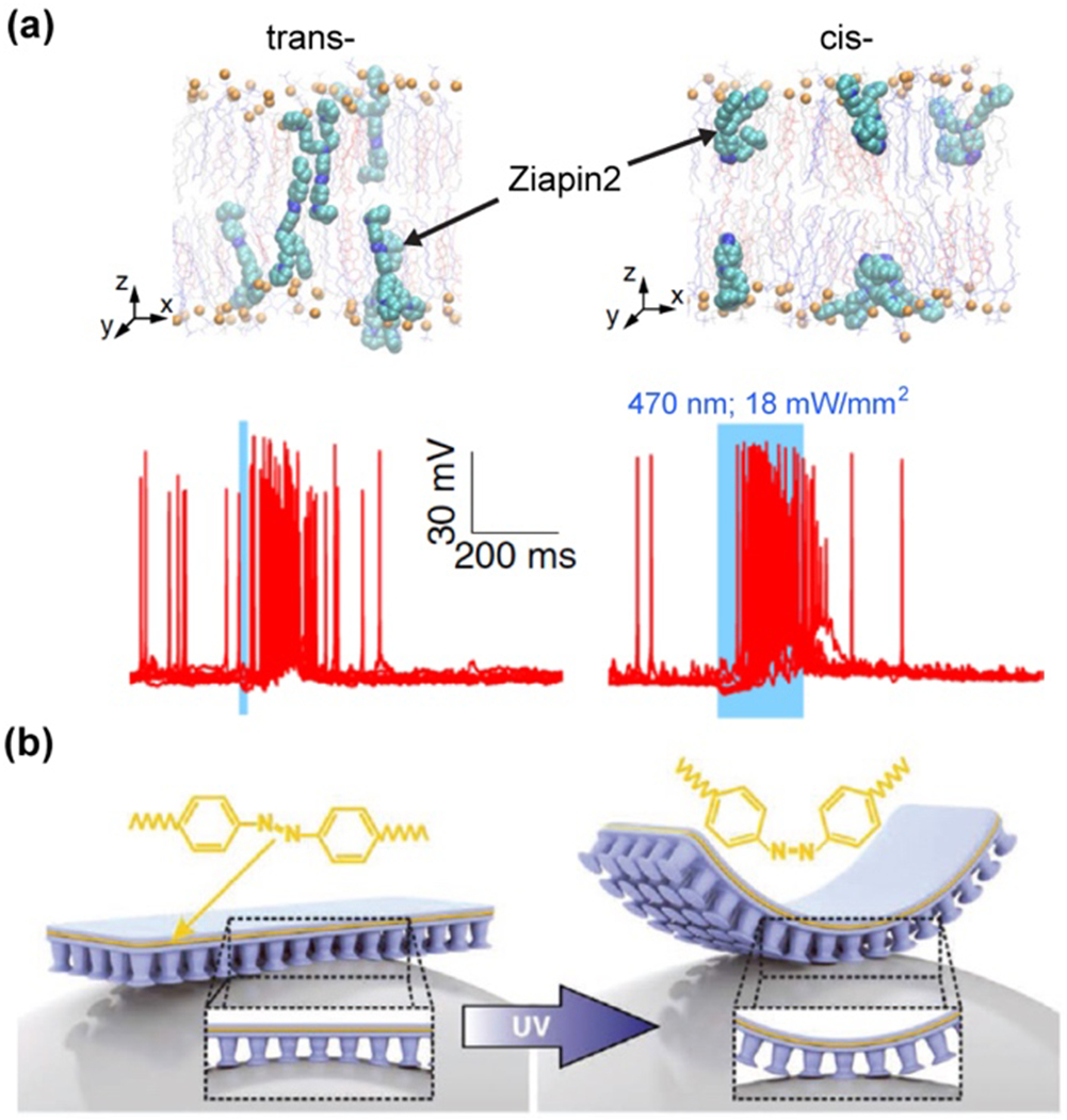
Photoisomerization-triggered neuromodulation. (a) Top: snapshots from MD simulations of a membrane-bound photoswitch, Ziapin2, in trans- and cis-conformations. Bottom: current-clamp traces from neurons incubated with Ziapin2. Illumination period is indicated with cyan shading. Reproduced from Ref.564 with permission from Springer Nature, copyright 2020. (b) Schematic of how photoisomerization can induce appreciable mechanical deformations in a material, useful for applications such as switchable adhesions and robotic actuators. Reproduced from Ref.565 with permission from Wiley, copyright 2019.
b). Optogenetics.
Optogenetics refers to a suite of techniques involving the genetic engineering of organisms to display light-responsive properties. It has seen a massive amount of interest since the early 2000s, when the phototransducer rhodopsin was employed to activate neurons,570 and the light-gated ion channel channelrhodopsin-2 was used to depolarize cells.571 Subsequent developments took advantage of ligand-gated channels and photocaged ligands, e.g., DMNB-capsaicin and DMNTE-ATP, to optically control the relevant channels.572 Since then, optogenetic methods have also been extended to the light-oxygen-voltage (LOV) sensing domain of Avena sativa phototropin 1 (Fig. 25).573 In this method, light activation uncages a domain that interacts with PDZ domains; in effect, allowing optical control over protein recruitment. This method, dubbed tuneable light-interacting protein tags (TULIPs), has been employed to great effect in studying cell mechanics by modulating actin severing by the protein cofilin,574 microtubule gliding assays,575 cell adhesion via switchable extracellular matrix,576 as well as force generation enacted via RhoA signaling.577, 578
Figure 25.
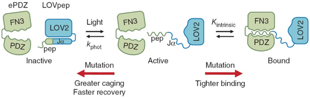
Schematic of LOVpep-based optogenetic dimerization. Illumination exposes the PDZ-binding domain of LOV2, thereby causing dimerization with PDZ domain proteins. Reproduced from Ref.573 with permission from Springer Nature, copyright 2012.
Because of optogenetics and other light-activated techniques in bioelectronics, the development of small, biocompatible light sources is of great interest. Micron-scale LEDs, for instance, have shown promise due to their small size and integrability,579 and they have been applied to neural modulation using optogenetics.580 They also function credibly as components of closed-loop systems,581 and have recently been validated for that purpose.4 Such devices should also prove feasible for use in photoswitching and photouncaging applications, such as controlled neurotransmitter release.
c). Upconversion.
Upconversion is the process wherein two photons of low frequency are absorbed by a structure and a single photon of higher frequency is emitted. Upconverting nanoparticles (UCNPs) are typically formed through heavy doping of trivalent lanthanides, especially Yb3+ and Tm3+.582 UCNPs with these dopants are particularly useful in biology, as they can absorb from within the so-called NIR-I window at 700-950 nm, where light has the greatest tissue penetration depth.583 The emission wavelengths can then be tuned to various desirable wavelengths in the visible range.584 This property has been used to enable NIR vision in mice, by complexing UCNPs with rods and cones.535 UCNPs have also been applied in conjunction with optogenetics, to overcome the depth limit imposed by the allowable wavelengths for optogenetic functionalization.585
These applications do not specifically involve bioelectronics, but they present a general template that will undoubtedly prove useful in the future: NIR light is used to access deep tissues and is upconverted to higher frequency light by UCNPs acting as intermediaries in the relevant tissues. These higher frequency photons can then be used to trigger bioelectrical signal generation and transmission, increasing their versatility and reducing the invasiveness of the overall therapy.
7.2.3. Magnetic processes in bioelectrical chemistry
Historically, the influence of magnetic fields on chemical reactions has been assumed to be nonexistent for most practical purposes.586 With a few notable examples, namely the radical pair mechanism,587–589 there is a paucity of proposed means by which external magnetic fields may inject enough energy into a system to induce an appreciable change in reaction outcomes or kinetics, particularly in the context of biochemical reactions.590 When measurable impacts of sub-Tesla magnetic fields have been observed, most notably in the case of enzymatic ATP synthesis rates,591 reproduction of these results has been elusive.592 The development of magnetic nanoparticles, however, has revitalized the possibility of magnetic stimuli to biology, with a few recent advances deserving particular attention.
Magnetic nanoparticles can be synthesized using a variety of metals and metal oxides, with iron, nickel, and cobalt being common choices.593 At room temperature, the magnetic moments of ferromagnetic particles below a material-dependent size threshold become small enough that they can be flipped by thermal fluctuations. They then have a net zero magnetic moment, but very high magnetic susceptibility (superparamagnetism).594 When a sample of particles are exposed to an alternating magnetic field (AMF), typically at radio frequencies, the induced oscillations have a heating effect that has been employed to kill cancer cells (magnetodynamic therapy),595 as well as activate transient receptor potential (TRP) channels.596 This TRP activation has been further applied to stimulate neurons both in vitro60, 596 and in vivo.60, 597 Recently, an elegant design was demonstrated for the remotely-controlled chemomagnetic modulation of neurons, where thermally-responsive liposomes (phase transition temperature, 43 °C) released chemical payloads (e.g., hM3D(Gq) ligand clozapine N-oxide, endogenous dopamine receptor D1 agonist) upon AMF application (Fig. 26a).61 This has allowed for magnetically-triggered motivated behaviors and sociability in mouse models (Fig. 26b). Magnetic nanoparticles with other shapes, such as hollow ones have been engineered for magnetically controlled drug release.593, 598 These examples highlight the recurring theme of novel forms of energy input to spatiotemporally control drug release.
Figure 26.
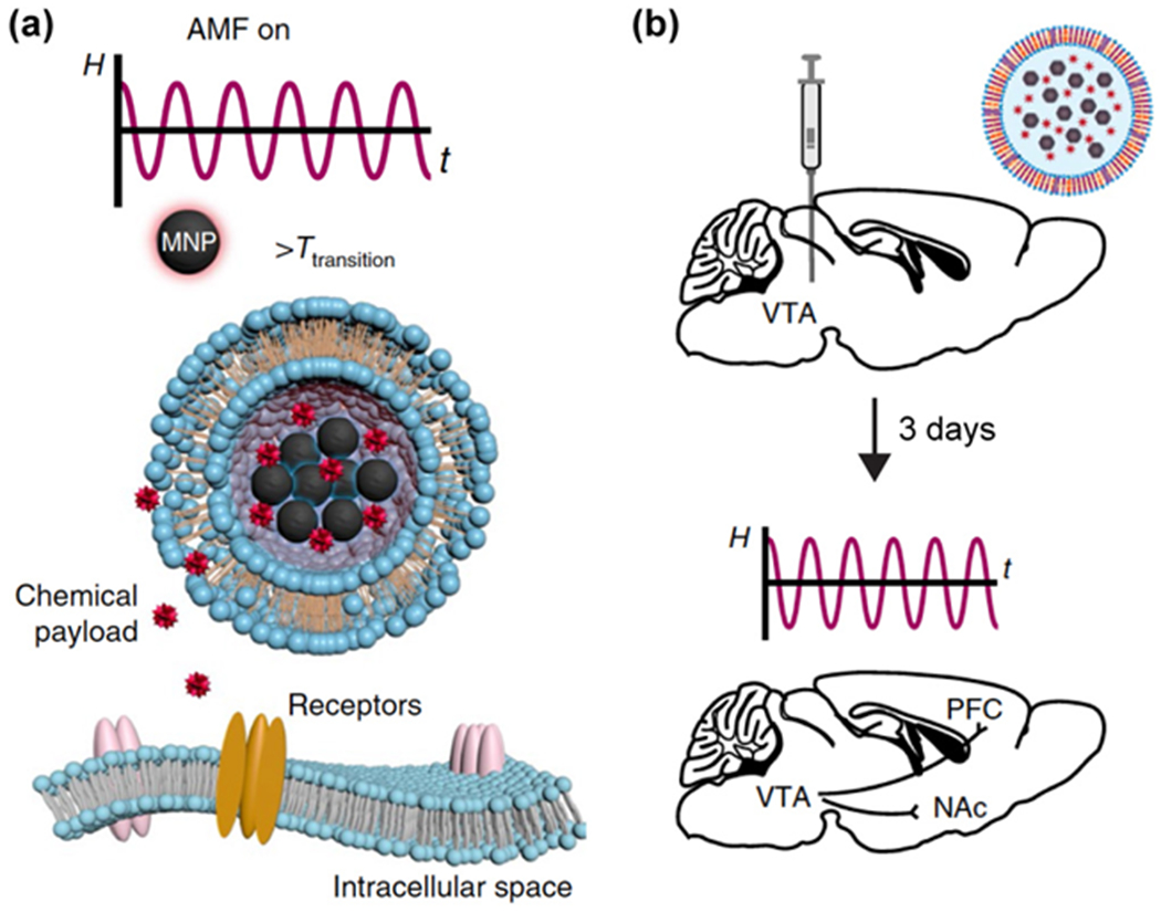
Schematic of remotely controlled chemomagnetic neuromodulation. (a) Magnetically responsive liposomes release chemical payloads upon magnetic heating and stimulate the receptors. (b) The liposomes can be injected into the ventral tegmental area, a region typically used for motivated behavior, reward and depression studies. (a) and (b) Reproduced from Ref.61 with permission from Springer Nature, copyright 2019.
7.3. Biomimetic Chemistry
Biomimetic materials comprise a large and active area of interest, focused on materials that aim to replicate some facet of biology. Some biomimetic materials are designed to only match a specific property, for example, soft substrates that approximate in vivo extracellular matrix more closely than glass599 but are otherwise quite chemically different from their biological counterparts. On the other hand, there exist biomimetics that are nearly identical to biological substances but for certain key differences, such as peptoids, which contain similar backbone structures to polypeptides but whose chemistry is entirely altered by having side chains substituted on backbone nitrogen atoms instead of alpha carbon atoms.600, 601
A key advantage offered by biomimetic materials is that, by their definition, they are based on designs that have been well-validated over the entire history of evolution. For bioelectronic applications, there is the additional benefit of their being more likely – although not guaranteed – to integrate nondestructively with biological targets. Despite this promise of reduced invasiveness, they may also be more resistant to biological degradation and able to operate in environments not accessible to strictly natural substances. For instance, certain biomimetics may operate in extreme temperature or pH conditions. Finally, many biomimetics are adaptable in two senses of the term. In one sense, the modular nature of biomimetic polymers enables large and versatile design spaces. In the other sense, they can also yield devices that automatically adjust themselves to suit their environments. This latter possibility was recently demonstrated with an artificial heart valve that adjusts its shape to maintain functionality with pediatric patients as they grow (Fig. 27a and b).602
Figure 27.
Biomimetic targets and designs. (a) Schematic showing conformation of geometrically adaptable heart valve when implanted in a juvenile sheep, in the unextended conformation. (b) Schematic showing conformation of geometrically adaptable heart valve when implanted in mature sheep. In this case, the needed pulmonary valve dimensions are 1.8x larger than the juvenile case. (a) and (b) Reproduced from Ref.602 with permission from the American Association for the Advancement of Science, copyright 2020. (c) Electric eel-mimicking hydrogel array. Red gel is high concentration NaCl, blue gel is low concentration NaCl, green gel is cation-selective, and yellow gel is anion-selective. Reproduced from Ref.605 with permission from Springer Nature, copyright 2017.
Considering the fascination Michael Faraday had with electric eels,603 it is perhaps fitting that researchers have recently turned to electric eels (Fig. 27c) as inspiration for next-generation power sources.604, 605 Briefly, Electrophorus electricus supports the production of potential differences up to 600 V and short-circuit currents near 1 A,606 with stacks of electrocytes – electrically active cells. The functionality of electrocytes comes from their ability to selectively modulate Na+ and K+ ion channel activity at the anterior and posterior ends. During activation, K+ efflux is reduced at the posterior end only, while Na+ influx is increased at the same region. This alters the total transcellular potential, that is, the potential across both the posterior and anterior areas, to about 150 mV. To recapitulate this behavior, the authors of a recent report designed a sequence of four hydrogels that contain alternating high concentration NaCl and low concentration NaCl, interdigitated by cation selective and anion selective gels that act as semipermeable membranes. When the full sequence of gels is placed in contact with each other, Na+ flows through the cation selective gel and Cl− flows through the anion selective gel, so that the resulting potential across the entire series was observed as high as 185 mV. While the total size of these biomimetic hydrogel stacks is not yet competitive with the size of the electrocytes that inspired them, these results are encouraging.
In the case of electronic plants, the “biomimetic template” is literal, rather than aspirational – plant structures are used as part of the fabrication process. This allows for the complex interlocking designs of plant structures to be replicated comparably easily. One example of this is seen in the production of conductive xylem wires and logic gates, made by immersing a cut rose in PEDOT-S:H solution.607 Such designs have also been employed to create plant tissue/conductive xylem supercapacitors.608 As the field of biomimetic and bioinspired materials continues to grow, there are certain to be similar keen analogies drawn between what biology already does and what can be incorporated into bioelectronics design.
7.4. Bioelectrocatalysis
The field of bioelectrocatalysis is drawing growing interest, as it promises to yield renewable energy materials that are also environmentally sustainable in their manufacture. Much of the focus of this field has centered on systems that function like either biomass fuel cells or solar energy.74, 609 Both approaches rely on similar components, namely, an electrocatalytic site, a means of charge transport to the electrode, and the electrode itself. Redox proteins and cofactors use a wide variety of both organic and metal centers in electrocatalysis, enabling the use of H2, glucose, or light as energy sources.
Electron transfer – from redox site to electrode – is the key process in bioelectrocatalysis (Fig. 28a). Under certain circumstances, namely that the distance from redox site to electrode is less than 2 nm,75 electrons can transfer directly from one to the other. This mechanism is called direct electron transfer (DET). While DET systems thus require less components than other strategies, the distance requirement places major restrictions on the design of the electrocatalytic site and the electrode, and the overall throughput is limited to what can be achieved with a single layer of sites.74, 75 This restriction can be partially lifted by direct wiring of redox sites and electrodes, which has recently been demonstrated using metalloprotein-prion domain protein chimera nanowires (Fig. 28b).610 Such methods, however, come with the caveat that such wiring schemes entail additional complexity for the system. Mediated electron transfer (MET) uses redox mediators to shuttle electrons from electrocatalytic site to electrode. This opens up the list of viable redox proteins, as mediators can access cryptic redox sites,74 and allows for more redox sites per electrode area. Designs using MET also frequently make use of inert polymer media, which can improve the stability of the overall device.74
Figure 28.
Chemical considerations in electron transfer and electrode selection for bioelectrocatalysis. (a) Direct electron transfer (DET) and mediated electron transfer (MET) schemes. DET is shown both wired and unwired. Reproduced from Ref.75 with permission from Springer Nature, copyright 2020. (b) A view of a protein chimera nanowire used for wiring in a synthetic redox film. Reproduced from Ref.610 with permission from Springer Nature, copyright 2016. (c) Diagram of how enhanced wettability of electrode surface can improve the electrochemical performance of a catalyst. Reproduced from Ref.612 with permission from the Wiley, copyright 2014.
Finally, the electrode selection can also have an impact on electrocatalytic performance. Surface chemistry, for example surface wettability (Fig. 28c), and topography each play important roles in ensuring good contact between the electrocatalyst and electrode.75, 611, 612 Additionally, the bioelectrochemical reaction may only take place on certain substrates, e.g., with microbes that harvest energy through iron oxidation or sulfate reduction.613
7.5. Biologically derived materials for bioelectronic systems
Recent years have seen a growing interest in materials that can be derived directly from biological sources, including plant biomass and animal sources. This owes itself to several factors. First, the raw materials are readily available: the primary components in plant biomass, cellulose and lignin, are among the most abundant biopolymers on the planet. Chitin, which is obtained from fungal, arthropod, and other sources, is also ubiquitous. As such, they are inexpensive and easy to procure. Additionally, they are derived from renewable sources, and the raw materials are biodegradable, making the manufacture of biomass-based materials potentially more environmentally friendly than fossil or mineral materials.
Cellulose is composed of β-1,4 linked d-glucose subunits (Fig. 29a). In many plant cell walls, cellulose is synthesized into nanofibers, which can vary in organization from species to species.614 Processing of these plant materials can yield additional nanostructures, with a great deal of recent attention focusing on cellulose nanocrystals. On its own, cellulose and its derivatives are good insulators, however, the high concentration of surface hydroxyl groups allows for a number of functionalization techniques that can endow such materials with capabilities relevant to bioelectronics. Nanocellulose materials integrated with carbon nanomaterials (nanotubes and graphene) have yielded flexible supercapacitors with high capacitance retention, even after being subjected to large deformations.615–617 Likewise, nanocellulose has been combined with conductive polymers PPy (Fig 29b), PANI, and PEDOT to yield supercapacitor devices.618–621 Such supercapacitors are immensely useful in bioelectronics, primarily as energy storage devices.622 To that end, they have been used in wearable technologies, integrated into clothing, and implanted.623
Figure 29.
Nanofibrillar cellulose and lignin form good substrates for bioelectronic supercapacitors. (a) Photograph of nanocellulose fibrillar paper and molecular structures for different types of nanocellulose fibers. (b) SEM image of PPy-nanocellulose fiber composite material. (a) and (b) Reproduced from Ref.621 with permission from the American Chemical Society, copyright 2015. (c) SEM image of lignin-derived carbon nanofiber mat. (d) 3D visualization of lignin-derived carbon nanofiber maps obtained from computed tomography. (c) and (d) Reproduced from Ref.628 under the terms of the Creative Commons Attribution License from the Royal Society of Chemistry, copyright 2019.
The structure of lignin is considerably more variable than that of cellulose: whereas the latter is well-defined as a polymer of glucose, the structure and molecular composition of lignin is highly heterogeneous (Fig. 29c and d). Nevertheless, its abundance and structural properties make it an attractive target for bioelectronic devices. As a photocatalyst, lignin hybrids with ZnO, TiO2, CeO2, and CuO have been found to improve photocatalytic depollution.624 Furthermore, lignin integrates well with conductive polymers for photovoltaic applications. The high content of aromatic structures in lignin and derivatives aid in hole transport, a fact that has been exploited to improve performance in PEDOT-based photovoltaics.625, 626 Like nanocellulose, lignin nanofibers have also served as a structural basis for supercapacitor devices.627, 628 Although we are not aware of any biological applications of lignin-based photocatalysts or photoelectrochemical stimuli in the existing literature, these materials show promise as low-cost devices that may enhance biological integration compared to artificially derived substrates.
Other biologically derived materials for electronics include chitosan, as well as reflectins and eumelanins obtained from cephalopods.629 Chitosan is a derivative of the polysaccharide chitin, which is among the most widely available biopolymers and is therefore a cost-effective and biocompatible material for bioelectronics.630 In the bioelectronic context, chitosan is frequently derivatized further into maleic chitosan and proline chitosan.631 Chitosan conductivity arises from proton mobility, so chitosans fall within the bioprotonics class of ionotronics.632, 633 As evidence of this, chitosan-based FET devices have been fabricated on SiO2 with palladium hydride contacts used to measure the protonic current.634
Biopolymers derived from cephalopods have attracted considerable interest on account of the wide variety of intriguing material behaviors squid skin can demonstrate, including sophisticated thermal regulation635 and colour changing.636 Reflectins, which constitute a family of proteins that are only found in cephalopods, are the primary component responsible for colour changing.637 In addition to their applicability to adaptive colour and camouflage, reflectins have been coaxed into self-assembly to form nanoparticles and films.638, 639 Studies of reflectin conductivity have found them to be bioprotonics,640 and they have been employed to form bioprotonic transistors.641, 642 Eumelanins comprise another protein family that can be found in cephalopod ink and also possess interesting electrical properties. In particular, hydrated thin films of eumelanins demonstrate conductivity that has been attributed to protonic conductivity as well as electrochemical reactions,643 that is, they are simultaneously bioprotonics and electrochemically active. The relative contributions of the protonic and electrochemical currents remain unclear, however, and it has been suggested that melanins behave as nearly purely protonic devices.644 Together with chitosan and reflectin, these three materials, which are all relevant to cephalopod physiology, compose a promising class of bioprotonics, and are likely to be incorporated into novel devices and materials with unique responsiveness.
7.6. Computational approaches to bioelectronics
Computational approaches have a long record of success in chemical and materials discovery. Large combinatorial libraries and high-throughput discovery techniques, for instance, take advantage of chemical information processing (cheminformatics) for both data handling and candidate identification.645–648 Similarly, in silico modeling of structures can rapidly narrow down a field of promising candidates, without requiring experimental validation for every possibility – a prospect that quickly becomes untenable as the size of the library grows.649 A functional example of this has been displayed with photoswitchable molecules, as discussed in section 7.2.2. In order to ensure that further experiments would be worthwhile, DiFrancesco et al. conducted molecular dynamics experiments to verify that their target molecule, Ziapin2, would integrate with cell membranes and still undergo cis-trans photoisomerization.564
The incredible success of computational methods for electronic structure have enabled a more precise understanding and characterization of new developments in organic electronics, including organic semiconductors and photovoltaic.156, 650 The principles of “molecular design,” in which functional improvements arise from fine tuning of the relevant molecules, rely in part on our ability to efficiently compute the effects of modifications to various moieties of those molecules. Of particular interest to bioelectronic applications are the frontier orbital energies, solubility characteristics, and morphological stability of organic electronics.
Machines that are capable of learning have been actively studied since the 1950’s.651 However, a series of high-profile achievements in the early 2010’s, coupled with the advent of practical implementations of deep learning,439, 652 have led machine learning (ML) to the forefront of academic interest in recent years. Proposed and actual applications of machine learning techniques have proliferated in most areas of the physical and life sciences, from particle physics beyond the Standard Model653 to pathology diagnosis from medical images.654, 655
As an illustrative example, we may consider neural decoding. Neural decoding is the process of converting records of brain activity into an understanding of both normal and pathological brain functions. As such, it relies heavily on signal processing, clustering, and other tasks ideally suited to machine learning.656 In principle, the information decoded by machine learning provides insights into the representational content of those signals. While this assertion is epistemologically suspect,657 such methods have produced functional results. For example, comprehensible machine-generated speech was recently derived from neural patterns,658 and the means to both control659 and receive660 sensory feedback from bionic arms have been reported. To further understand the architecture of the brain, we will require better means to measure neural signaling, therefore the future of neuronal decoding is intertwined with the development of bioelectronic sensors.
With the goal of more precisely tuneable bioelectronics – both in terms of design and effect – in mind, machine learning has shown great promise in this field. Recently, ML has been combined with molecular dynamics simulations to obtain structural and material properties of amorphous Si at low computational cost compared to ab initio methods.661 Similarly, ML has been employed to devise an interatomic potential for Si that improves on empirically derived force fields in describing a number of observable properties, e.g., phase changes by different mechanisms.662 ML has also been used to predict sets of structures that will be similar and stable under given thermodynamic constraints.653, 663
7.7. Living bioelectronics
Continued progress in bioelectronics and related areas of research has led to developments in a nascent field that combines biological cells with electronic systems in a genuinely synergistic fashion. This field of “living bioelectronics,” also referred as “biohybrid robots” in the literature,664, 665 promises to combine the strengths of artificial robots – information density, reliability, and processing speed – with the strengths of biology – error-tolerance, energy-efficiency, and dynamic responses.666 Currently, there is a good deal of attention on the development of reliable and scaleable actuators for living bioelectronics. There are a number of proposed paths towards this goal, ranging from biomimetic composites of synthetic parts548 to self-assembling “tissues” of engineered cells.664, 665
The artificial approach makes extensive use of piezoelectric motors,667 shape memory alloys,209 and dielectric elastomers.668 There have been notable recent successes for piezoelectric669 and shape memory alloy-based209, 670 actuators in soft robotics,671 as well as a striking biomorphic design of artificial wings using dielectric elastomers.672 For applications in living bioelectronics, however, engineered tissues have drawn a great deal of attention.665 This is due to many factors, including the multiple functionality of cells665 and the potential for implants where the interactions with the biological environment are features that are designed, rather than minimized or tolerated.504, 673 To that end, systems that incorporate cell-based actuators into their design include artificial muscles,664 light674 and electricity-responsive536 coordinated undulations in a synthetic ray, and motors powered by the optically-controlled swimming of bacteria.675
As fundamentally robotic systems, living bioelectronics would be autonomous biological systems controlled by computer hardware, a premise that carries with its major implications for biomedical ethics676–678 as well as computer/information ethics.679, 680 It is not sufficient to call for ethical clarity at some unspecified point in the future. Given the potential global impact of living bioelectronics and the cost mistakes in this field may incur,681, 682 it is vital that all developments are firmly based on an ethical foundation.
8. Concluding remarks
Chemistry offers numerous opportunities for improving bioelectronics into devices with excellent biocompatibility, biomechanical properties and electronic/optoelectronic performance. This goal requires considerable cross-disciplinary efforts; when done successfully, it blends materials science, bioengineering, and electronic device/system fabrication, along with new developments in chemistry. The chemistry aspects accelerate important advances in how we think about bioelectronics. As we have seen, devices may include components that are organic or inorganic, and which function as conductors or semiconductors. The characteristics of each type of material allow for bioelectronics that acts on length scales from the molecular to the organismal, with durations from nanoseconds to months or even years.
In the near future, we expect that chemical considerations will be employed to great success in formulating synergistic combinations of some of the recent discoveries highlighted here. This may happen in two main ways. In one approach, materials with similar chemistries but varying functionalities can be used in tandem to create devices that expand the range of capabilities beyond either material. The other approach entails combining materials with much more differing chemical properties, to either attenuate the weaknesses of each other, or to bestow the eventual device with multiple distinct functionalities. It is likely that both approaches will yield highly significant insights. Hard-soft composites offer a mechanical example of this principle, in which the combination of stiff and compliant materials can both mitigate the impacts of mechanical mismatch between device and tissue, as well as offering new routes of sensing or stimulation.
Furthermore, developments in disciplines that are adjacent to bioelectronics offer a wealth of possible applications to bioelectronics. For instance, a common theme is the use of energy input methods with good spatiotemporal resolution – acoustic, optical, and magnetic impulses – to dramatically improve the localization of various therapies. There is enormous potential for bioelectronic discoveries based on perspectives from multiple disciplines. This is as valid for bioelectronics collaborations within the natural sciences as it is for collaborations between scientists and other areas of inquiry, such as ethics or sociology. In all cases, advances in chemistry will enable many of the most critical insights.
Acknowledgements:
This work is supported by the Air Force Office of Scientific Research (AFOSR FA9550-18-1-0503), US Army Research Office (W911NF-18-1-0042), US Office of Naval Research (N000141612958), the National Science Foundation (NSF 1848613), and the National Institutes of Health (NIH NS101488).
Footnotes
Conflicts of interest: The authors declare no conflicts of interest.
References
- 1.Zhang A and Lieber CM, Chemical Reviews, 2016, 116, 215–257. [DOI] [PMC free article] [PubMed] [Google Scholar]
- 2.Chortos A, Liu J and Bao Z, Nature Materials, 2016, 15, 937–950. [DOI] [PubMed] [Google Scholar]
- 3.Jonsson A, Inal S, Uguz I, Williamson AJ, Kergoat L, Rivnay J, Khodagholy D, Berggren M, Bernard C, Malliaras GG and Simon DT, Proceedings of the National Academy of Sciences, 2016, 113, 9440. [DOI] [PMC free article] [PubMed] [Google Scholar]
- 4.Mickle AD, Won SM, Noh KN, Yoon J, Meacham KW, Xue Y, McIlvried LA, Copits BA, Samineni VK, Crawford KE, Kim DH, Srivastava P, Kim BH, Min S, Shiuan Y, Yun Y, Payne MA, Zhang J, Jang H, Li Y, Lai HH, Huang Y, Park SI, Gereau RW and Rogers JA, Nature, 2019, 565, 361–365. [DOI] [PMC free article] [PubMed] [Google Scholar]
- 5.Cingolani E, Goldhaber JI and Marbán E, Nature Reviews Cardiology, 2018, 15, 139–150. [DOI] [PMC free article] [PubMed] [Google Scholar]
- 6.Feiner R, Engel L, Fleischer S, Malki M, Gal I, Shapira A, Shacham-Diamand Y and Dvir T, Nature Materials, 2016, 15, 679–685. [DOI] [PMC free article] [PubMed] [Google Scholar]
- 7.Yacoub MH and McLeod C, Nature Reviews Cardiology, 2018, 15, 770–779. [DOI] [PubMed] [Google Scholar]
- 8.Freedman B, Boriani G, Glotzer TV, Healey JS, Kirchhof P and Potpara TS, Nature Reviews Cardiology, 2017, 14, 701–714. [DOI] [PubMed] [Google Scholar]
- 9.Hong G, Yang X, Zhou T and Lieber CM, Curr Opin Neurobiol, 2018, 50, 33–41. [DOI] [PMC free article] [PubMed] [Google Scholar]
- 10.Fu TM, Hong G, Zhou T, Schuhmann TG, Viveros RD and Lieber CM, Nat Methods, 2016, 13, 875–882. [DOI] [PubMed] [Google Scholar]
- 11.Hong GS, Fu TM, Qiao M, Viveros RD, Yang X, Zhou T, Lee JM, Park HG, Sanes JR and Lieber CM, Science, 2018, 360, 1447-+. [DOI] [PMC free article] [PubMed] [Google Scholar]
- 12.Hong GS and Lieber CM, Nature Reviews Neuroscience, 2019, 20, 330–345. [DOI] [PMC free article] [PubMed] [Google Scholar]
- 13.Gao W, Emaminejad S, Nyein HYY, Challa S, Chen K, Peck A, Fahad HM, Ota H, Shiraki H, Kiriya D, Lien DH, Brooks GA, Davis RW and Javey A, Nature, 2016, 529, 509–514. [DOI] [PMC free article] [PubMed] [Google Scholar]
- 14.Bandodkar AJ, Jeang WJ, Ghaffari R and Rogers JA, Annual Review of Analytical Chemistry, 2019, 12, 1–22. [DOI] [PubMed] [Google Scholar]
- 15.Kalantar-Zadeh K, Berean KJ, Ha N, Chrimes AF, Xu K, Grando D, Ou JZ, Pillai N, Campbell JL, Brkljača R, Taylor KM, Burgell RE, Yao CK, Ward SA, McSweeney CS, Muir JG and Gibson PR, Nature Electronics, 2018, 1, 79–87. [Google Scholar]
- 16.Wang L, Xie S, Wang Z, Liu F, Yang Y, Tang C, Wu X, Liu P, Li Y, Saiyin H, Zheng S, Sun X, Xu F, Yu H and Peng H, Nature Biomedical Engineering, 2019, DOI: 10.1038/s41551-019-0462-8. [DOI] [PubMed] [Google Scholar]
- 17.Lacour SP, Courtine G and Guck J, Nature Reviews Materials, 2016, 1. [Google Scholar]
- 18.Wenger N, Moraud EM, Gandar J, Musienko P, Capogrosso M, Baud L, Le Goff CG, Barraud Q, Pavlova N, Dominici N, Minev IR, Asboth L, Hirsch A, Duis S, Kreider J, Mortera A, Haverbeck O, Kraus S, Schmitz F, DiGiovanna J, van den Brand R, Bloch J, Detemple P, Lacour SP, Bézard E, Micera S and Courtine G, Nature Medicine, 2016, 22, 138–145. [DOI] [PMC free article] [PubMed] [Google Scholar]
- 19.Wagner FB, Mignardot J-B, Le Goff-Mignardot CG, Demesmaeker R, Komi S, Capogrosso M, Rowald A, Seáñez I, Caban M, Pirondini E, Vat M, McCracken LA, Heimgartner R, Fodor I, Watrin A, Seguin P, Paoles E, Van Den Keybus K, Eberle G, Schurch B, Pralong E, Becce F, Prior J, Buse N, Buschman R, Neufeld E, Kuster N, Carda S, von Zitzewitz J, Delattre V, Denison T, Lambert H, Minassian K, Bloch J and Courtine G, Nature, 2018, 563, 65–71. [DOI] [PubMed] [Google Scholar]
- 20.Formento E, Minassian K, Wagner F, Mignardot JB, Le Goff-Mignardot CG, Rowald A, Bloch J, Micera S, Capogrosso M and Courtine G, Nature Neuroscience, 2018, 21, 1728–1741. [DOI] [PMC free article] [PubMed] [Google Scholar]
- 21.Gill ML, Grahn PJ, Calvert JS, Linde MB, Lavrov IA, Strommen JA, Beck LA, Sayenko DG, Van Straaten MG, Drubach DI, Veith DD, Thoreson AR, Lopez C, Gerasimenko YP, Edgerton VR, Lee KH and Zhao KD, Nature Medicine, 2018, 24, 1677–1682. [DOI] [PubMed] [Google Scholar]
- 22.Acarón Ledesma H, Li X, Carvalho-de-Souza JL, Wei W, Bezanilla F and Tian B, Nature Nanotechnology, 2019, 14, 645–657. [DOI] [PMC free article] [PubMed] [Google Scholar]
- 23.Chen R, Canales A and Anikeeva P, Nature Reviews Materials, 2017, 2, 1–16. [DOI] [PMC free article] [PubMed] [Google Scholar]
- 24.Obidin N, Tasnim F and Dagdeviren C, Advanced Materials, 2019, 1901482, 1–26. [DOI] [PubMed] [Google Scholar]
- 25.Frank JA, Antonini MJ and Anikeeva P, Nature Biotechnology, 2019, 37, 1013–1023. [DOI] [PMC free article] [PubMed] [Google Scholar]
- 26.Rivnay J, Wang H, Fenno L, Deisseroth K and Malliaras GG, Sci Adv, 2017, 3, e1601649. [DOI] [PMC free article] [PubMed] [Google Scholar]
- 27.Cai P, Leow WR, Wang X, Wu YL and Chen X, Adv Mater, 2017, 29. [DOI] [PubMed] [Google Scholar]
- 28.Wang M, Mi G, Shi D, Bassous N, Hickey D and Webster TJ, Advanced Functional Materials, 2018, 28, 1700905. [Google Scholar]
- 29.Won SM, Song E, Zhao J, Li J, Rivnay J and Rogers JA, Adv Mater, 2018, 30, e1800534. [DOI] [PubMed] [Google Scholar]
- 30.Wang T, Wang M, Yang L, Li Z, Loh XJ and Chen X, Adv Mater, 2020, 32, e1905522. [DOI] [PubMed] [Google Scholar]
- 31.Gao W, Ota H, Kiriya D, Takei K and Javey A, Acc Chem Res, 2019, 52, 523–533. [DOI] [PubMed] [Google Scholar]
- 32.Ray TR, Choi J, Bandodkar AJ, Krishnan S, Gutruf P, Tian L, Ghaffari R and Rogers JA, Chem Rev, 2019, 119, 5461–5533. [DOI] [PubMed] [Google Scholar]
- 33.Moffa AH, Martin D, Alonzo A, Bennabi D, Blumberger DM, Benseñor IM, Daskalakis Z, Fregni F, Haffen E, Lisanby SH, Padberg F, Palm U, Razza LB, Sampaio-Jr B, Loo C and Brunoni AR, Progress in Neuro-Psychopharmacology and Biological Psychiatry, 2020, 99. [DOI] [PubMed] [Google Scholar]
- 34.Dai XC, Hong GS, Gao T and Lieber CM, Accounts of Chemical Research, 2018, 51, 309–318. [DOI] [PMC free article] [PubMed] [Google Scholar]
- 35.Fu TM, Hong GS, Viveros RD, Zhou T and Lieber CM, Proceedings of the National Academy of Sciences of the United States of America, 2017, 114, E10046–E10055. [DOI] [PMC free article] [PubMed] [Google Scholar]
- 36.Fu TM, Hong GS, Zhou T, Schuhmann TG, Viveros RD and Lieber CM, Nature Methods, 2016, 13, 875-+. [DOI] [PubMed] [Google Scholar]
- 37.Hong GS, Fu TM, Zhou T, Schuhmann TG, Huang JL and Lieber CM, Nano Letters, 2015, 15, 6979–6984. [DOI] [PubMed] [Google Scholar]
- 38.Jiang Y, Li X, Liu B, Yi J, Fang Y, Shi F, Gao X, Sudzilovsky E, Parameswaran R, Koehler K, Nair V, Yue J, Guo K, Fang Y, Tsai H-M, Freyermuth G, Wong RCS, Kao C-M, Chen C-T, Nicholls AW, Wu X, Shepherd GMG and Tian B, Nature Biomedical Engineering, 2018, 2, 508–521. [DOI] [PMC free article] [PubMed] [Google Scholar]
- 39.Someya T, Bao Z and Malliaras GG, Nature, 2016, 540, 379–385. [DOI] [PubMed] [Google Scholar]
- 40.Li Q, Nan KW, Le Floch P, Lin ZW, Sheng H, Blum TS and Liu J, Nano Letters, 2019, 19, 5781–5789. [DOI] [PubMed] [Google Scholar]
- 41.Cohen-Karni T, Timko BP, Weiss LE and Lieber CM, Proceedings of the National Academy of Sciences of the United States of America, 2009, 106, 7309–7313. [DOI] [PMC free article] [PubMed] [Google Scholar]
- 42.Duan X, Gao R, Xie P, Cohen-Karni T, Qing Q, Choe HS, Tian B, Jiang X and Lieber CM, Nature Nanotechnology, 2012, 7, 174–179. [DOI] [PMC free article] [PubMed] [Google Scholar]
- 43.Tian B, Cohen-Karni T, Qing Q, Duan X, Xie P and Lieber CM, Science, 2010, 329, 830–834. [DOI] [PMC free article] [PubMed] [Google Scholar]
- 44.Xiang L, Chen K, Yan R, Li W and Xu K, Nature Methods, 2020, DOI: 10.1038/s41592-020-0793-0. [DOI] [PMC free article] [PubMed] [Google Scholar]
- 45.Phillips R and Quake SR, Physics Today, 2006, 59, 38–43. [Google Scholar]
- 46.Musk E, Journal of Medical Internet Research, 2019, 21, e16194–e16194. [DOI] [PMC free article] [PubMed] [Google Scholar]
- 47.Drake KL, Wise KD, Farraye J, Anderson DJ and BeMent SL, IEEE Transactions on Biomedical Engineering, 1988, 35, 719–732. [DOI] [PubMed] [Google Scholar]
- 48.Jones KE, Campbell PK and Normann RA, Annals of Biomedical Engineering, 1992, 20, 423–437. [DOI] [PubMed] [Google Scholar]
- 49.Maynard EM, Nordhausen CT and Normann RA, Electroencephalography and Clinical Neurophysiology, 1997, 102, 228–239. [DOI] [PubMed] [Google Scholar]
- 50.Vetter RJ, Williams JC, Hetke JF, Nunamaker EA and Kipke DR, IEEE Transactions on Biomedical Engineering, 2004, 51, 896–904. [DOI] [PubMed] [Google Scholar]
- 51.Wise KD, IEEE Engineering in Medicine and Biology Magazine, 2005, 24, 22–29. [DOI] [PubMed] [Google Scholar]
- 52.Campbell PK, Jones KE, Huber RJ, Horch KW and Normann RA, IEEE Transactions on Biomedical Engineering, 1991, 38, 758–768. [DOI] [PubMed] [Google Scholar]
- 53.Spoendlin H and Schrott A, Hearing Research, 1989, 43, 25–38. [DOI] [PubMed] [Google Scholar]
- 54.Jonas JB, Schmidt AM, Muller-Bergh JA, Schlotzer-Schrehardt UM and Naumann GOH, Investigative Ophthalmology and Visual Science, 1992, 33, 2012–2018. [PubMed] [Google Scholar]
- 55.Willett FR, Deo DR, Avansino DT, Rezaii P, Hochberg LR, Henderson JM and Shenoy KV, Cell, 2020, 181, 396–409.e326. [DOI] [PMC free article] [PubMed] [Google Scholar]
- 56.Eichenlaub J-B, Jarosiewicz B, Saab J, Franco B, Kelemen J, Halgren E, Hochberg LR and Cash SS, Cell Reports, 2020, 31, 107581. [DOI] [PMC free article] [PubMed] [Google Scholar]
- 57.Obaid A, Hanna M-E, Wu Y-W, Kollo M, Racz R, Angle MR, Müller J, Brackbill N, Wray W, Franke F, Chichilnisky EJ, Hierlemann A, Ding JB, Schaefer AT and Melosh NA, Science Advances, 2020, 6, eaay2789. [DOI] [PMC free article] [PubMed] [Google Scholar]
- 58.Zhang Y, Zheng Z, Yu M, Hsu C, Berthiaume EA, Pan H, Zhang X, Stieg AZ, Wu B, Wang H, Ting K and Soo C, ACS Applied Materials & Interfaces, 2018, 10, 15449–15460. [DOI] [PMC free article] [PubMed] [Google Scholar]
- 59.Zhang Y, Mickle AD, Gutruf P, McIlvried LA, Guo H, Wu Y, Golden JP, Xue Y, Grajales-Reyes JG, Wang X, Krishnan S, Xie Y, Peng D, Su CJ, Zhang F, Reeder JT, Vogt SK, Huang Y, Rogers JA and Gereau RW, Science Advances, 2019, 5, 1–12. [DOI] [PMC free article] [PubMed] [Google Scholar]
- 60.Chen R, Romero G, Christiansen MG, Mohr A and Anikeeva P, Science, 2015, 347, 1477–1480. [DOI] [PubMed] [Google Scholar]
- 61.Rao SY, Chen R, LaRocca AA, Christiansen MG, Senko AW, Shi CH, Chiang PH, Varnavides G, Xue J, Zhou Y, Park S, Ding RH, Moon J, Feng GP and Anikeeva P, Nature Nanotechnology, 2019, 14, 967-+. [DOI] [PMC free article] [PubMed] [Google Scholar]
- 62.Jiang Y, Parameswaran R, Li X, Carvalho-de-Souza JL, Gao X, Meng L, Bezanilla F, Shepherd GMG and Tian B, Nature Protocols, 2019, 14, 1339–1376. [DOI] [PMC free article] [PubMed] [Google Scholar]
- 63.Parameswaran R, Koehler K, Rotenberg MY, Burke MJ, Kim J, Jeong K-Y, Hissa B, Paul MD, Moreno K, Sarma N, Hayes T, Sudzilovsky E, Park H-G and Tian B, Proc Natl Acad Sci USA, 2019, 116, 413–421. [DOI] [PMC free article] [PubMed] [Google Scholar]
- 64.Yoo S, Hong S, Choi Y, Park JH and Nam Y, ACS Nano, 2014, 8, 8040–8049. [DOI] [PubMed] [Google Scholar]
- 65.Carvalho-de-Souza JL, Pinto BI, Pepperberg DR and Bezanilla F, Biophysical Journal, 2018, 114, 283–288. [DOI] [PMC free article] [PubMed] [Google Scholar]
- 66.Carvalho-de-Souza JL, Treger JS, Dang B, Kent SB, Pepperberg DR and Bezanilla F, Neuron, 2015, 86, 207–217. [DOI] [PMC free article] [PubMed] [Google Scholar]
- 67.Jiang Y, Carvalho-de-Souza JL, Wong RCS, Luo Z, Isheim D, Zuo X, Nicholls AW, Jung IW, Yue J, Liu D-J, Wang Y, De Andrade V, Xiao X, Navrazhnykh L, Weiss DE, Wu X, Seidman DN, Bezanilla F and Tian B, Nature Materials, 2016, 15, 1023–1030. [DOI] [PMC free article] [PubMed] [Google Scholar]
- 68.Kubanek J, Shukla P, Das A, Baccus SA and Goodman MB, Journal of Neuroscience, 2018, 38, 3081–3091. [DOI] [PMC free article] [PubMed] [Google Scholar]
- 69.Plonsey R and Barr RC, Bioelectricity: a quantitative approach, Springer Science & Business Media, 2007. [Google Scholar]
- 70.Savtchenko LP, Poo MM and Rusakov DA, Nature Reviews Neuroscience, 2017, 18, 598–612. [DOI] [PubMed] [Google Scholar]
- 71.Yuk H, Lu B and Zhao X, Chemical Society Reviews, 2019, 48, 1642–1667. [DOI] [PubMed] [Google Scholar]
- 72.Sanjuan-Alberte P, Alexander MR, Hague RJM and Rawson FJ, Bioelectronic Medicine, 2018, 4, 1–7. [DOI] [PMC free article] [PubMed] [Google Scholar]
- 73.Choi C, Ashby DS, Butts DM, DeBlock RH, Wei Q, Lau J and Dunn B, Nature Reviews Materials, 2020, 5, 5–19. [Google Scholar]
- 74.Ruff A, Conzuelo F and Schuhmann W, Nature Catalysis, 2020, 3, 214–224. [Google Scholar]
- 75.Chen H, Dong F and Minteer SD, Nature Catalysis, 2020, 3, 225–244. [Google Scholar]
- 76.Rudolph TK and Freeman BA, Science Signaling, 2009, 2, re7–re7. [DOI] [PMC free article] [PubMed] [Google Scholar]
- 77.Dickinson BC and Chang CJ, Nature Chemical Biology, 2011, 7, 504–511. [DOI] [PMC free article] [PubMed] [Google Scholar]
- 78.Burton A, Obaid SN, Vazquez-Guardado A, Schmit MB, Stuart T, Cai L, Chen Z, Kandela I, Haney CR, Waters EA, Cai H, Rogers JA, Lu L and Gutruf P, Proc Natl Acad Sci U S A, 2020, 117, 2835–2845. [DOI] [PMC free article] [PubMed] [Google Scholar]
- 79.Lu L, Gutruf P, Xia L, Bhatti DL, Wang X, Vazquez-Guardado A, Ning X, Shen X, Sang T, Ma R, Pakeltis G, Sobczak G, Zhang H, Seo D.-o., Xue M, Yin L, Chanda D, Sheng X, Bruchas MR and Rogers JA, Proc Natl Acad Sci U S A, 2018, 115, E1374–E1383. [DOI] [PMC free article] [PubMed] [Google Scholar]
- 80.Zhang Z and Yates JT, Chemical Reviews, 2012, 112, 5520–5551. [DOI] [PubMed] [Google Scholar]
- 81.Vilan A and Cahen D, Chemical Reviews, 2017, 117, 4624–4666. [DOI] [PubMed] [Google Scholar]
- 82.Pankove JI, Optical processes in semiconductors, Prentice-Hall, Englewood Cliffs, N.J.,, 1971. [Google Scholar]
- 83.Mayer KM and Hafner JH, Chem Rev, 2011, 111, 3828–3857. [DOI] [PubMed] [Google Scholar]
- 84.Jauffred L, Samadi A, Klingberg H, Bendix PM and Oddershede LB, Chem Rev, 2019, 119, 8087–8130. [DOI] [PubMed] [Google Scholar]
- 85.Donner JS, Thompson SA, Kreuzer MP, Baffou G and Quidant R, Nano Lett, 2012, 12, 2107–2111. [DOI] [PubMed] [Google Scholar]
- 86.Bai T and Gu N, Small, 2016, 12, 4590–4610. [DOI] [PubMed] [Google Scholar]
- 87.Dalby MJ, Gadegaard N, Herzyk P, Sutherland D, Agheli H, Wilkinson CDW and Curtis ASG, Journal of Cellular Biochemistry, 2007, 102, 1234–1244. [DOI] [PubMed] [Google Scholar]
- 88.Beard P, Interface Focus, 2011, 1, 602–631. [DOI] [PMC free article] [PubMed] [Google Scholar]
- 89.Park S, Frank JA and Anikeeva P, Nature Biomedical Engineering, 2018, 2, 471–472. [DOI] [PubMed] [Google Scholar]
- 90.Dipalo M, Melle G, Lovato L, Jacassi A, Santoro F, Caprettini V, Schirato A, Alabastri A, Garoli D, Bruno G, Tantussi F and De Angelis F, Nat Nanotechnol, 2018, 13, 965–971. [DOI] [PubMed] [Google Scholar]
- 91.Li Q, Lu N, Wang L and Fan C, Small Methods, 2018, 2, 1700263. [Google Scholar]
- 92.Schöning MJ and Poghossian A, Analyst, 2002, 127, 1137–1151. [DOI] [PubMed] [Google Scholar]
- 93.Fromherz P, Offenhausser A, Vetter T and Weis J, Science, 1991, 252, 1290. [DOI] [PubMed] [Google Scholar]
- 94.Bernards DA and Malliaras GG, Advanced Functional Materials, 2007, 17, 3538–3544. [Google Scholar]
- 95.Rivnay J, Inal S, Salleo A, Owens RM, Berggren M and Malliaras GG, Nature Reviews Materials, 2018, 3. [Google Scholar]
- 96.Khodagholy D, Rivnay J, Sessolo M, Gurfinkel M, Leleux P, Jimison LH, Stavrinidou E, Herve T, Sanaur S, Owens RM and Malliaras GG, Nature Communications, 2013, 4, 1–6. [DOI] [PMC free article] [PubMed] [Google Scholar]
- 97.Ghittorelli M, Lingstedt L, Romele P, Crăciun NI, Kovács-Vajna ZM, Blom PWM and Torricelli F, Nature Communications, 2018, 9, 1441. [DOI] [PMC free article] [PubMed] [Google Scholar]
- 98.Jakešová M, Sjöström TA, Đerek V, Poxson D, Berggren M, Głowacki ED and Simon DT, npj Flexible Electronics, 2019, 3. [Google Scholar]
- 99.Isaksson J, Kjäll P, Nilsson D, Robinson N, Berggren M and Richter-Dahlfors A, Nature Materials, 2007, 6, 673–679. [DOI] [PubMed] [Google Scholar]
- 100.Williamson A, Rivnay J, Kergoat L, Jonsson A, Inal S, Uguz I, Ferro M, Ivanov A, Sjöström TA, Simon DT, Berggren M, Malliaras GG and Bernard C, Advanced Materials, 2015, 27, 3138–3144. [DOI] [PubMed] [Google Scholar]
- 101.Seitanidou M, Blomgran R, Pushpamithran G, Berggren M and Simon DT, Advanced Healthcare Materials, 2019, 8, 1900813. [DOI] [PubMed] [Google Scholar]
- 102.Berggren M, Crispin X, Fabiano S, Jonsson MP, Simon DT, Stavrinidou E, Tybrandt K and Zozoulenko I, Advanced Materials, 2019, 31, 1805813. [DOI] [PubMed] [Google Scholar]
- 103.Arbring Sjöström T, Berggren M, Gabrielsson EO, Janson P, Poxson DJ, Seitanidou M and Simon DT, Advanced Materials Technologies, 2018, 3, 1700360. [Google Scholar]
- 104.Jonsson A, Song Z, Nilsson D, Meyerson BA, Simon DT, Linderoth B and Berggren M, Science Advances, 2015, 1, 1–6. [DOI] [PMC free article] [PubMed] [Google Scholar]
- 105.Cobo A, Sheybani R and Meng E, Advanced Healthcare Materials, 2015, 4, 969–982. [DOI] [PubMed] [Google Scholar]
- 106.Meng E and Hoang T, Advanced Drug Delivery Reviews, 2012, 64, 1628–1638. [DOI] [PMC free article] [PubMed] [Google Scholar]
- 107.Boyden ES, Zhang F, Bamberg E, Nagel G and Deisseroth K, Nature Neuroscience, 2005, 8, 1263–1268. [DOI] [PubMed] [Google Scholar]
- 108.Levitz J, Broichhagen J, Leippe P, Konrad D, Trauner D and Isacoff EY, Proceedings of the National Academy of Sciences of the United States of America, 2017, 114, E3546–E3554. [DOI] [PMC free article] [PubMed] [Google Scholar]
- 109.Delbeke J, Hoffman L, Mols K, Braeken D and Prodanov D, Frontiers in Neuroscience, 2017, 11, 1–20. [DOI] [PMC free article] [PubMed] [Google Scholar]
- 110.Seymour JP, Wu F, Wise KD and Yoon E, Microsystems and Nanoengineering, 2017, 3, 1–16. [DOI] [PMC free article] [PubMed] [Google Scholar]
- 111.Qazi R, Gomez AM, Castro DC, Zou Z, Sim JY, Xiong Y, Abdo J, Kim CY, Anderson A, Lohner F, Byun SH, Chul Lee B, Jang KI, Xiao J, Bruchas MR and Jeong JW, Nature Biomedical Engineering, 2019, 3, 655–669. [DOI] [PubMed] [Google Scholar]
- 112.Wang N, Journal of Physics D: Applied Physics, 2017, 50. [DOI] [PMC free article] [PubMed] [Google Scholar]
- 113.Li Y, Xiao Y and Liu C, Chemical Reviews, 2017, 117, 4376–4421. [DOI] [PubMed] [Google Scholar]
- 114.Hernandez M, Patzig J, Mayoral SR, Costa KD, Chan JR and Casaccia P, Journal of Neuroscience, 2016, 36, 806–813. [DOI] [PMC free article] [PubMed] [Google Scholar]
- 115.Zhao W, Hanson L, Lou H-Y, Akamatsu M, Chowdary PD, Santoro F, Marks JR, Grassart A, Drubin DG, Cui Y and Cui B, Nature Nanotechnology, 2017, 12, 750–756. [DOI] [PMC free article] [PubMed] [Google Scholar]
- 116.Guimarães CF, Gasperini L, Marques AP and Reis RL, Nature Reviews Materials, 2020, DOI: 10.1038/s41578-019-0169-1, 1–20.33078077 [DOI] [Google Scholar]
- 117.Salatino JW, Ludwig KA, Kozai TDY and Purcell EK, Nature Biomedical Engineering, 2017, 1, 862–877. [DOI] [PMC free article] [PubMed] [Google Scholar]
- 118.Copits BA, Pullen MY and Gereau RW, PAIN, 2016, 157, 2424–2433. [DOI] [PMC free article] [PubMed] [Google Scholar]
- 119.McFarland DJ and Wolpaw JR, Communications of the ACM, 2011, 54, 60–66. [DOI] [PMC free article] [PubMed] [Google Scholar]
- 120.Micera S, Caleo M, Chisari C, Hummel FC and Pedrocchi A, Neuron, 2020, 105, 604–620. [DOI] [PubMed] [Google Scholar]
- 121.Rogers JA, Someya T and Huang Y, Science, 2010, 327, 1603–1607. [DOI] [PubMed] [Google Scholar]
- 122.Xue Z, Song H, Rogers JA, Zhang Y and Huang Y, Advanced Materials, 2019, 1902254, 1–32. [DOI] [PubMed] [Google Scholar]
- 123.Zhu C, Du D and Lin Y, Biosensors and Bioelectronics, 2017, 89, 43–55. [DOI] [PubMed] [Google Scholar]
- 124.Taboada GM, Yang K, Pereira MJN, Liu SS, Hu Y, Karp JM, Artzi N and Lee Y, Nature Reviews Materials, 2020, DOI: 10.1038/s41578-019-0171-7. [DOI] [Google Scholar]
- 125.Koo J, MacEwan MR, Kang SK, Won SM, Stephen M, Gamble P, Xie Z, Yan Y, Chen YY, Shin J, Birenbaum N, Chung S, Kim SB, Khalifeh J, Harburg DV, Bean K, Paskett M, Kim J, Zohny ZS, Lee SM, Zhang R, Luo K, Ji B, Banks A, Lee HM, Huang Y, Ray WZ and Rogers JA, Nature Medicine, 2018, 24, 1830–1836. [DOI] [PubMed] [Google Scholar]
- 126.Irimia-Vladu M, Chem. Soc. Rev, 2014, 43, 588–610. [DOI] [PubMed] [Google Scholar]
- 127.Hoppe A, Güldal NS and Boccaccini AR, Biomaterials, 2011, 32, 2757–2774. [DOI] [PubMed] [Google Scholar]
- 128.Han S, Kim J, Won SM, Ma Y, Kang D, Xie Z, Lee K-T, Chung HU, Banks A, Min S, Heo SY, Davies CR, Lee JW, Lee C-H, Kim BH, Li K, Zhou Y, Wei C, Feng X, Huang Y and Rogers JA, Sci. Transl. Med, 2018, 10, eaan4950. [DOI] [PMC free article] [PubMed] [Google Scholar]
- 129.Parameswaran R, Carvalho-De-Souza JL, Jiang Y, Burke MJ, Zimmerman JF, Koehler K, Phillips AW, Yi J, Adams EJ, Bezanilla F and Tian B, Nature Nanotechnology, 2018, 13, 260–266. [DOI] [PMC free article] [PubMed] [Google Scholar]
- 130.Rotenberg MY, Yamamoto N, Schaumann EN, Matino L, Santoro F and Tian B, Proc Natl Acad Sci USA, 2019, 116, 22531–22539. [DOI] [PMC free article] [PubMed] [Google Scholar]
- 131.Patolsky F, Zheng G and Lieber CM, Nat Protoc, 2006, 1, 1711–1724. [DOI] [PubMed] [Google Scholar]
- 132.Shimoda T, Matsuki Y, Furusawa M, Aoki T, Yudasaka I, Tanaka H, Iwasawa H, Wang D, Miyasaka M and Takeuchi Y, Nature, 2006, 440, 783–786. [DOI] [PubMed] [Google Scholar]
- 133.Tran PD, Artero V and Fontecave M, Energy Environ. Sci., 2010, 3, 727–747. [Google Scholar]
- 134.Hwang SW, Tao H, Kim DH, Cheng H, Song JK, Rill E, Brenckle MA, Panilaitis B, Won SM, Kim YS, Song YM, Yu KJ, Ameen A, Li R, Su Y, Yang M, Kaplan DL, Zakin MR, Slepian MJ, Huang Y, Omenetto FG and Rogers JA, Science, 2012, 337, 1640–1644. [DOI] [PMC free article] [PubMed] [Google Scholar]
- 135.Fang Y, Jiang Y, Acaron Ledesma H, Yi J, Gao X, Weiss DE, Shi F and Tian B, Nano Letters, 2018, 18, 4487–4492. [DOI] [PMC free article] [PubMed] [Google Scholar]
- 136.Hochbaum AI, Gargas D, Hwang YJ and Yang P, Nano Letters, 2009, 9, 3550–3554. [DOI] [PubMed] [Google Scholar]
- 137.Chiappini C, De Rosa E, Martinez JO, Liu X, Steele J, Stevens MM and Tasciotti E, Nature Materials, 2015, 14, 532–539. [DOI] [PMC free article] [PubMed] [Google Scholar]
- 138.Salonen J and Mäkilä E, Advanced Materials, 2018, 30, 1703819. [DOI] [PubMed] [Google Scholar]
- 139.Orosco MM, Pacholski C and Sailor MJ, Nature Nanotechnology, 2009, 4, 255–258. [DOI] [PMC free article] [PubMed] [Google Scholar]
- 140.Vilensky R, Bercovici M and Segal E, Advanced Functional Materials, 2015, 25, 6725–6732. [Google Scholar]
- 141.Acaron Ledesma H and Tian B, J. Mater. Chem. B, 2017, 5, 4276–4289. [DOI] [PubMed] [Google Scholar]
- 142.Kim S and Cahoon JF, Accounts of Chemical Research, 2019, 52, 3511–3520. [DOI] [PubMed] [Google Scholar]
- 143.Fang Y, Jiang Y, Cherukara MJ, Shi F, Koehler K, Freyermuth G, Isheim D, Narayanan B, Nicholls AW, Seidman DN, Sankaranarayanan SKRS and Tian B, Nature Communications, 2017, 8, 2014. [DOI] [PMC free article] [PubMed] [Google Scholar]
- 144.Luo Z, Jiang Y, Myers BD, Isheim D, Wu J, Zimmerman JF, Wang Z, Li Q, Wang Y, Chen X, Dravid VP, Seidman DN and Tian B, Science, 2015, 348, 1451–1455. [DOI] [PubMed] [Google Scholar]
- 145.Hill DJ, Teitsworth TS, Ritchie ET, Atkin JM and Cahoon JF, ACS Nano, 2018, 12, 10554–10563. [DOI] [PubMed] [Google Scholar]
- 146.Kim S, Hill DJ, Pinion CW, Christesen JD, McBride JR and Cahoon JF, ACS Nano, 2017, 11, 4453–4462. [DOI] [PubMed] [Google Scholar]
- 147.Pinion CW, Christesen JD and Cahoon JF, J. Mater. Chem. C, 2016, 4, 3890–3897. [Google Scholar]
- 148.Gao X, Jiang Y, Lin Y, Kim KH, Fang Y, Yi J, Meng L, Lee HC, Lu Z, Leddy O, Zhang R, Tu Q, Feng W, Nair V, Griffin PJ, Shi F, Shekhawat GS, Dinner AR, Park HG and Tian B, Sci Adv, 2020, 6, eaay2760. [DOI] [PMC free article] [PubMed] [Google Scholar]
- 149.Dhanaraj G, Springer handbook of crystal growth, Springer, Heidelberg ; New York, 2010. [Google Scholar]
- 150.Borle WN and Bagai RK, Journal of Crystal Growth, 1976, 36, 259–262. [Google Scholar]
- 151.Li C, Guo C, Fitzpatrick V, Ibrahim A, Zwierstra MJ, Hanna P, Lechtig A, Nazarian A, Lin SJ and Kaplan DL, Nature Reviews Materials, 2020, 5, 61–81. [Google Scholar]
- 152.Chang J-K, Fang H, Bower CA, Song E, Yu X and Rogers JA, Proc Natl Acad Sci USA, 2017, 114, E5522–E5529. [DOI] [PMC free article] [PubMed] [Google Scholar]
- 153.Irimia-Vladu M, Glowacki ED, Sariciftci NS and Bauer S, Green Materials for Electronics, Wiley-VCH Verlag GmbH & Co. KGaA, Weinheim, Germany, 2017. [Google Scholar]
- 154.Park J-H, Gu L, von Maltzahn G, Ruoslahti E, Bhatia SN and Sailor MJ, Nature Materials, 2009, 8, 331–336. [DOI] [PMC free article] [PubMed] [Google Scholar]
- 155.Dekeyser CM, Buron CC, Derclaye SR, Jonas AM, Marchand-Brynaert J and Rouxhet PG, Journal of Colloid and Interface Science, 2012, 378, 77–82. [DOI] [PubMed] [Google Scholar]
- 156.Wilcox DA, Snaider J, Mukherjee S, Yuan L, Huang L, Savoie BM and Boudouris BW, Soft Matter, 2019, 15, 1413–1422. [DOI] [PubMed] [Google Scholar]
- 157.Shin J, Liu Z, Bai W, Liu Y, Yan Y, Xue Y, Kandela I, Pezhouh M, MacEwan MR, Huang Y, Ray WZ, Zhou W and Rogers JA, Science Advances, 2019, 5, eaaw1899. [DOI] [PMC free article] [PubMed] [Google Scholar]
- 158.Shin J, Yan Y, Bai W, Xue Y, Gamble P, Tian L, Kandela I, Haney CR, Spees W, Lee Y, Choi M, Ko J, Ryu H, Chang J-K, Pezhouh M, Kang S-K, Won SM, Yu KJ, Zhao J, Lee YK, MacEwan MR, Song S-K, Huang Y, Ray WZ and Rogers JA, Nature Biomedical Engineering, 2019, 3, 37–46. [DOI] [PubMed] [Google Scholar]
- 159.Chiappini C, Martinez JO, De Rosa E, Almeida CS, Tasciotti E and Stevens MM, ACS Nano, 2015, 9, 5500–5509. [DOI] [PMC free article] [PubMed] [Google Scholar]
- 160.Bai W, Shin J, Fu R, Kandela I, Lu D, Ni X, Park Y, Liu Z, Hang T, Wu D, Liu Y, Haney CR, Stepien I, Yang Q, Zhao J, Nandoliya KR, Zhang H, Sheng X, Yin L, MacRenaris K, Brikha A, Aird F, Pezhouh M, Hornick J, Zhou W and Rogers JA, Nat Biomed Eng, 2019, 3, 644–654. [DOI] [PubMed] [Google Scholar]
- 161.Hu S, Shaner MR, Beardslee JA, Lichterman M, Brunschwig BS and Lewis NS, Science, 2014, 344, 1005–1009. [DOI] [PubMed] [Google Scholar]
- 162.Peled A, Pevzner A, Peretz Soroka H and Patolsky F, J Nanobiotechnol, 2014, 12, 7. [DOI] [PMC free article] [PubMed] [Google Scholar]
- 163.Fang H, Yu KJ, Gloschat C, Yang Z, Song E, Chiang C-H, Zhao J, Won SM, Xu S, Trumpis M, Zhong Y, Han SW, Xue Y, Xu D, Choi SW, Cauwenberghs G, Kay M, Huang Y, Viventi J, Efimov IR and Rogers JA, Nature Biomedical Engineering, 2017, 1, 0038. [DOI] [PMC free article] [PubMed] [Google Scholar]
- 164.Chen YW, Prange JD, Dühnen S, Park Y, Gunji M, Chidsey CED and McIntyre PC, Nature Materials, 2011, 10, 539–544. [DOI] [PubMed] [Google Scholar]
- 165.Ji L, McDaniel MD, Wang S, Posadas AB, Li X, Huang H, Lee JC, Demkov AA, Bard AJ, Ekerdt JG and Yu ET, Nature Nanotechnology, 2015, 10, 84–90. [DOI] [PubMed] [Google Scholar]
- 166.Mathieson K, Loudin J, Goetz G, Huie P, Wang L, Kamins TI, Galambos L, Smith R, Harris JS, Sher A and Palanker D, Nature Photon, 2012, 6, 391–397. [DOI] [PMC free article] [PubMed] [Google Scholar]
- 167.Lorach H, Goetz G, Smith R, Lei X, Mandel Y, Kamins T, Mathieson K, Huie P, Harris J, Sher A and Palanker D, Nature Medicine, 2015, 21, 476–482. [DOI] [PMC free article] [PubMed] [Google Scholar]
- 168.Wang L, Mathieson K, Kamins TI, Loudin JD, Galambos L, Goetz G, Sher A, Mandel Y, Huie P, Lavinsky D, Harris JS and Palanker DV, Journal of Neural Engineering, 2012, 9, 046014. [DOI] [PMC free article] [PubMed] [Google Scholar]
- 169.Yokota T, Nakamura T, Kato H, Mochizuki M, Tada M, Uchida M, Lee S, Koizumi M, Yukita W, Takimoto A and Someya T, Nature Electronics, 2020, 3, 113–121. [Google Scholar]
- 170.Patolsky F, Zheng G, Hayden O, Lakadamyali M, Zhuang X and Lieber CM, Proc Natl Acad Sci U S A, 2004, 101, 14017–14022. [DOI] [PMC free article] [PubMed] [Google Scholar]
- 171.Cui Y, Science, 2001, 293, 1289–1292. [DOI] [PubMed] [Google Scholar]
- 172.Cui Y, Zhong Z, Wang D, Wang WU and Lieber CM, Nano Letters, 2003, 3, 149–152. [Google Scholar]
- 173.Wu Y, Xiang J, Yang C, Lu W and Lieber CM, Nature, 2004, 430, 61–65. [DOI] [PubMed] [Google Scholar]
- 174.Zhao Y, Yao J, Xu L, Mankin MN, Zhu Y, Wu H, Mai L, Zhang Q and Lieber CM, Nano Letters, 2016, 16, 2644–2650. [DOI] [PubMed] [Google Scholar]
- 175.Zhao Y, You SS, Zhang A, Lee J-H, Huang J and Lieber CM, Nat. Nanotechnol, 2019, 14, 783–790. [DOI] [PubMed] [Google Scholar]
- 176.Fang H, Yu KJ, Gloschat C, Yang Z, Chiang CH, Zhao J, Won SM, Xu S, Trumpis M, Zhong Y, Song E, Han SW, Xue Y, Xu D, Cauwenberghs G, Kay M, Huang Y, Viventi J, Efimov IR and Rogers JA, Nat Biomed Eng, 2017, 1. [DOI] [PMC free article] [PubMed] [Google Scholar]
- 177.Fang H, Zhao J, Yu KJ, Song E, Farimani AB, Chiang CH, Jin X, Xue Y, Xu D, Du W, Seo KJ, Zhong Y, Yang Z, Won SM, Fang G, Choi SW, Chaudhuri S, Huang Y, Alam MA, Viventi J, Aluru NR and Rogers JA, Proc Natl Acad Sci U S A, 2016, 113, 11682–11687. [DOI] [PMC free article] [PubMed] [Google Scholar]
- 178.Li J, Song E, Chiang CH, Yu KJ, Koo J, Du H, Zhong Y, Hill M, Wang C, Zhang J, Chen Y, Tian L, Zhong Y, Fang G, Viventi J and Rogers JA, Proc Natl Acad Sci U S A, 2018, 115, E9542–E9549. [DOI] [PMC free article] [PubMed] [Google Scholar]
- 179.Veerbeek J and Huskens J, Small Methods, 2017, 1, 1700072. [Google Scholar]
- 180.Huang K, Duclairoir F, Pro T, Buckley J, Marchand G, Martinez E, Marchon J-C, De Salvo B, Delapierre G and Vinet F, ChemPhysChem, 2009, 10, 963–971. [DOI] [PubMed] [Google Scholar]
- 181.Fabre B, Accounts of Chemical Research, 2010, 43, 1509–1518. [DOI] [PubMed] [Google Scholar]
- 182.Fabre B, Li Y, Scheres L, Pujari SP and Zuilhof H, Angewandte Chemie International Edition, 2013, 52, 12024–12027. [DOI] [PubMed] [Google Scholar]
- 183.Yang Y, Ciampi S, Zhu Y and Gooding JJ, The Journal of Physical Chemistry C, 2016, 120, 13032–13038. [Google Scholar]
- 184.Liu H, Duclairoir F, Fleury B, Dubois L, Chenavier Y and Marchon J-C, Dalton Transactions, 2009, DOI: 10.1039/B901309A, 3793–3799. [DOI] [PubMed] [Google Scholar]
- 185.Vacher A, Auffray M, Barrière F, Roisnel T and Lorcy D, Organic Letters, 2017, 19, 6060–6063. [DOI] [PubMed] [Google Scholar]
- 186.Yzambart G, Fabre B and Lorcy D, Langmuir, 2012, 28, 3453–3459. [DOI] [PubMed] [Google Scholar]
- 187.Gao F and Teplyakov AV, Langmuir, 2017, 33, 8632–8639. [DOI] [PMC free article] [PubMed] [Google Scholar]
- 188.Feng W and Miller B, Langmuir, 1999, 15, 3152–3156. [Google Scholar]
- 189.Bunimovich YL, Shin YS, Yeo W-S, Amori M, Kwong G and Heath JR, J. Am. Chem. Soc, 2006, 128, 16323–16331. [DOI] [PMC free article] [PubMed] [Google Scholar]
- 190.Har-Lavan R, Yaffe O, Joshi P, Kazaz R, Cohen H and Cahen D, AIP Advances, 2012, 2, 012164. [Google Scholar]
- 191.Faber EJ, de Smet LCPM, Olthuis W, Zuilhof H, Sudhölter EJR, Bergveld P and van den Berg A, ChemPhysChem, 2005, 6, 2153–2166. [DOI] [PubMed] [Google Scholar]
- 192.Roth KM, Yasseri AA, Liu Z, Dabke RB, Malinovskii V, Schweikart K-H, Yu L, Tiznado H, Zaera F, Lindsey JS, Kuhr WG and Bocian DF, J. Am. Chem. Soc, 2003, 125, 505–517. [DOI] [PubMed] [Google Scholar]
- 193.Lee SH, Kang JS and Kim D, Materials (Basel), 2018, 11, 2557. [DOI] [PMC free article] [PubMed] [Google Scholar]
- 194.Peng W, Rupich SM, Shafiq N, Gartstein YN, Malko AV and Chabal YJ, Chemical Reviews, 2015, 115, 12764–12796. [DOI] [PubMed] [Google Scholar]
- 195.Politi J, Zappavigna S, Rea I, Grieco P, Caliò A, Luce A, Caraglia M and De Stefano L, Journal of Sensors, 2017, 2017, 6792396. [Google Scholar]
- 196.Pápa Z, Ramakrishnan SK, Martin M, Cloitre T, Zimányi L, Márquez J, Budai J, Tóth Z and Gergely C, Langmuir, 2016, 32, 7250–7258. [DOI] [PubMed] [Google Scholar]
- 197.Wang Z-H and Jin G, Colloids and Surfaces B: Biointerfaces, 2004, 34, 173–177. [DOI] [PubMed] [Google Scholar]
- 198.Aissaoui N, Bergaoui L, Landoulsi J, Lambert J-F and Boujday S, Langmuir, 2012, 28, 656–665. [DOI] [PubMed] [Google Scholar]
- 199.Hong Q, Rogero C, Lakey JH, Connolly BA, Houlton A and Horrocks BR, Analyst, 2009, 134, 593–601. [DOI] [PubMed] [Google Scholar]
- 200.Lee J-H, Zhang A, You SS and Lieber CM, Nano Letters, 2016, 16, 1509–1513. [DOI] [PubMed] [Google Scholar]
- 201.Li X, Chen X, Tan J, Liang X and Wu J, Analyst, 2017, 142, 586–590. [DOI] [PubMed] [Google Scholar]
- 202.Ji X, Wang H, Song B, Chu B and He Y, Frontiers in Chemistry, 2018, 6, 38. [DOI] [PMC free article] [PubMed] [Google Scholar]
- 203.Patolsky F, Timko BP, Yu G, Fang Y, Greytak AB, Zheng G and Lieber CM, Science, 2006, 313, 1100–1104. [DOI] [PubMed] [Google Scholar]
- 204.Zhang W, Tong L and Yang C, Nano Lett, 2012, 12, 1002–1006. [DOI] [PubMed] [Google Scholar]
- 205.Gan X, Zhao H and Quan X, Biosensors and Bioelectronics, 2017, 89, 56–71. [DOI] [PubMed] [Google Scholar]
- 206.Xiong M, Rong Q, Meng H.-m. and Zhang X.-b., Biosensors and Bioelectronics, 2017, 89, 212–223. [DOI] [PubMed] [Google Scholar]
- 207.Son D, Chae SI, Kim M, Choi MK, Yang J, Park K, Kale VS, Koo JH, Choi C, Lee M, Kim JH, Hyeon T and Kim D-H, Advanced Materials, 2016, 28, 9326–9332. [DOI] [PubMed] [Google Scholar]
- 208.Reynolds MF, Guimarães MHD, Gao H, Kang K, Cortese AJ, Ralph DC, Park J and McEuen PL, Science Advances, 2019, 5, eaat9476. [DOI] [PMC free article] [PubMed] [Google Scholar]
- 209.Huang X, Kumar K, Jawed MK, Mohammadi Nasab A, Ye Z, Shan W and Majidi C, Adv. Mater. Technol, 2019, 4, 1800540. [Google Scholar]
- 210.Kang K, Xie S, Huang L, Han Y, Huang PY, Mak KF, Kim C-J, Muller D and Park J, Nature, 2015, 520, 656–660. [DOI] [PubMed] [Google Scholar]
- 211.Datta I, Chae SH, Bhatt GR, Tadayon MA, Li B, Yu Y, Park C, Park J, Cao L, Basov DN, Hone J and Lipson M, Nature Photon, 2020, DOI: 10.1038/s41566-020-0590-4. [DOI] [Google Scholar]
- 212.Xie S, Tu L, Han Y, Huang L, Kang K, Lao KU, Poddar P, Park C, Muller DA, DiStasio RA and Park J, Science, 2018, 359, 1131–1136. [DOI] [PubMed] [Google Scholar]
- 213.Choi S, Tan SH, Li Z, Kim Y, Choi C, Chen P-Y, Yeon H, Yu S and Kim J, Nature Materials, 2018, 17, 335–340. [DOI] [PubMed] [Google Scholar]
- 214.Kim Y, Cruz SS, Lee K, Alawode BO, Choi C, Song Y, Johnson JM, Heidelberger C, Kong W, Choi S, Qiao K, Almansouri I, Fitzgerald EA, Kong J, Kolpak AM, Hwang J and Kim J, Nature, 2017, 544, 340–343. [DOI] [PubMed] [Google Scholar]
- 215.Bae S-H, Lu K, Han Y, Kim S, Qiao K, Choi C, Nie Y, Kim H, Kum HS, Chen P, Kong W, Kang B-S, Kim C, Lee J, Baek Y, Shim J, Park J, Joo M, Muller DA, Lee K and Kim J, Nature Nanotechnology, 2020, DOI: 10.1038/s41565-020-0633-5. [DOI] [PubMed] [Google Scholar]
- 216.Kong W, Li H, Qiao K, Kim Y, Lee K, Nie Y, Lee D, Osadchy T, Molnar RJ, Gaskill DK, Myers-Ward RL, Daniels KM, Zhang Y, Sundram S, Yu Y, Bae S.-h., Rajan S, Shao-Horn Y, Cho K, Ougazzaden A, Grossman JC and Kim J, Nature Materials, 2018, 17, 999–1004. [DOI] [PubMed] [Google Scholar]
- 217.Shin SR, Migliori B, Miccoli B, Li Y-C, Mostafalu P, Seo J, Mandla S, Enrico A, Antona S, Sabarish R, Zheng T, Pirrami L, Zhang K, Zhang YS, Wan K.-t., Demarchi D, Dokmeci MR and Khademhosseini A, Adv. Mater, 2018, 13. [DOI] [PMC free article] [PubMed] [Google Scholar]
- 218.Nurunnabi M, Biomedical applications of graphene and 2D nanomaterials, Elsevier, Cambridge, CA, 1st edition edn., 2019. [Google Scholar]
- 219.Wang F and Liu X, Chemical Society Reviews, 2009, 38, 976–989. [DOI] [PubMed] [Google Scholar]
- 220.Kang D, Kim TW, Kubota SR, Cardiel AC, Cha HG and Choi K-S, Chemical Reviews, 2015, 115, 12839–12887. [DOI] [PubMed] [Google Scholar]
- 221.Holtus T, Helmbrecht L, Hendrikse HC, Baglai I, Meuret S, Adhyaksa GWP, Garnett EC and Noorduin WL, Nat Chem, 2018, 10, 740–745. [DOI] [PubMed] [Google Scholar]
- 222.Montalti M, Cantelli A and Battistelli G, Chemical Society Reviews, 2015, 44, 4853–4921. [DOI] [PubMed] [Google Scholar]
- 223.Efros AL, Delehanty JB, Huston AL, Medintz IL, Barbic M and Harris TD, Nature Nanotechnology, 2018, 13, 278–288. [DOI] [PubMed] [Google Scholar]
- 224.Caglar M, Pandya R, Xiao J, Foster SK, Divitini G, Chen RYS, Greenham NC, Franze K, Rao A and Keyser UF, Nano Letters, 2019, 19, 8539–8549. [DOI] [PMC free article] [PubMed] [Google Scholar]
- 225.Nag OK, Stewart MH, Deschamps JR, Susumu K, Oh E, Tsytsarev V, Tang Q, Efros AL, Vaxenburg R, Black BJ, Chen Y, O’Shaughnessy TJ, North SH, Field LD, Dawson PE, Pancrazio JJ, Medintz IL, Chen Y, Erzurumlu RS, Huston AL and Delehanty JB, ACS Nano, 2017, 11, 5598–5613. [DOI] [PMC free article] [PubMed] [Google Scholar]
- 226.Cestellos-Blanco S, Zhang H and Yang PD, Faraday Discussions, 2019, 215, 54–65. [DOI] [PubMed] [Google Scholar]
- 227.Sakimoto KK, Wong AB and Yang PD, Science, 2016, 351, 74–77. [DOI] [PubMed] [Google Scholar]
- 228.Saldrnoto KK, Kornienko N and Yang PD, Accounts of Chemical Research, 2017, 50, 476–481. [DOI] [PubMed] [Google Scholar]
- 229.Zhang H, Liu H, Tian ZQ, Lu D, Yu Y, Cestellos-Blanco S, Sakimoto KK and Yang PD, Nature Nanotechnology, 2018, 13, 900-+. [DOI] [PubMed] [Google Scholar]
- 230.Guo JL, Suastegui M, Sakimoto KK, Moody VM, Xiao G, Nocera DG and Joshi NS, Science, 2018, 362, 813-+. [DOI] [PMC free article] [PubMed] [Google Scholar]
- 231.Wu X, Zhu XJ, Chong P, Liu JL, Andre LN, Ong KS, Brinson K, Mahdi AI, Li JC, Fenno LE, Wang HL and Hong GS, Proceedings of the National Academy of Sciences of the United States of America, 2019, 116, 26332–26342. [DOI] [PMC free article] [PubMed] [Google Scholar]
- 232.Sarkar D, Liu W, Xie X, Anselmo AC, Mitragotri S and Banerjee K, ACS Nano, 2014, 8, 3992–4003. [DOI] [PubMed] [Google Scholar]
- 233.Mak KF and Shan J, Nature Photon, 2016, 10, 216–226. [Google Scholar]
- 234.Wang L, Wang Y, Wong JI, Palacios T, Kong J and Yang HY, Small, 2014, 10, 1101–1105. [DOI] [PubMed] [Google Scholar]
- 235.Manzeli S, Allain A, Ghadimi A and Kis A, Nano Letters, 2015, 15, 5330–5335. [DOI] [PubMed] [Google Scholar]
- 236.Liu C, Kong D, Hsu PC, Yuan H, Lee HW, Liu Y, Wang H, Wang S, Yan K, Lin D, Maraccini PA, Parker KM, Boehm AB and Cui Y, Nat Nanotechnol, 2016, 11, 1098–1104. [DOI] [PubMed] [Google Scholar]
- 237.Choi C, Choi MK, Liu S, Kim MS, Park OK, Im C, Kim J, Qin X, Lee GJ, Cho KW, Kim M, Joh E, Lee J, Son D, Kwon SH, Jeon NL, Song YM, Lu N and Kim DH, Nature Communications, 2017, 8. [DOI] [PMC free article] [PubMed] [Google Scholar]
- 238.Gao N and Fang X, Chemical Reviews, 2015, 115, 8294–8343. [DOI] [PubMed] [Google Scholar]
- 239.Ong W-J, Tan L-L, Ng YH, Yong S-T and Chai S-P, Chemical Reviews, 2016, 116, 7159–7329. [DOI] [PubMed] [Google Scholar]
- 240.Zhang Z, Xu R, Wang Z, Dong M, Cui B and Chen M, ACS Appl. Mater. Interfaces, 2017, 9, 34736–34743. [DOI] [PubMed] [Google Scholar]
- 241.Huang J, Antonietti M and Liu J, J. Mater. Chem. A, 2014, 2, 7686–7693. [Google Scholar]
- 242.Liu J and Antonietti M, Energy Environ. Sci., 2013, 6, 1486. [Google Scholar]
- 243.Yang D, Zou H, Wu Y, Shi J, Zhang S, Wang X, Han P, Tong Z and Jiang Z, Ind. Eng. Chem. Res, 2017, 56, 6247–6255. [Google Scholar]
- 244.Appel JH, Li DO, Podlevsky JD, Debnath A, Green AA, Wang QH and Chae J, ACS Biomaterials Science & Engineering, 2016, 2, 361–367. [DOI] [PubMed] [Google Scholar]
- 245.Shah P, Narayanan TN, Li C-Z and Alwarappan S, Nanotechnology, 2015, 26, 315102. [DOI] [PubMed] [Google Scholar]
- 246.Teo WZ, Chng ELK, Sofer Z and Pumera M, Chemistry – A European Journal, 2014, 20, 9627–9632. [DOI] [PubMed] [Google Scholar]
- 247.Guiney LM, Wang X, Xia T, Nel AE and Hersam MC, ACS nano, 2018, 12, 6360–6377. [DOI] [PMC free article] [PubMed] [Google Scholar]
- 248.Chia HL, Latiff NM, Gusmão R, Sofer Z and Pumera M, Chemistry – A European Journal, 2019, 25, 2242–2249. [DOI] [PubMed] [Google Scholar]
- 249.Nakatsuka N, Yang KA, Abendroth JM, Cheung KM, Xu X, Yang H, Zhao C, Zhu B, Rim YS, Yang Y, Weiss PS, Stojanović MN and Andrews AM, Science, 2018, 362, 319–324. [DOI] [PMC free article] [PubMed] [Google Scholar]
- 250.Tang J, Qin N, Chong Y, Diao Y, Yiliguma Wang Z, Xue T, Jiang M, Zhang J and Zheng G, Nat Commun, 2018, 9, 786. [DOI] [PMC free article] [PubMed] [Google Scholar]
- 251.Chai S, Kim YJ and Lee W, Journal of Electroceramics - J ELECTROCERAM, 2006, 17, 909–912. [Google Scholar]
- 252.Jiang L, Lv F-C, Yang R, Hu D-C and Guo X, Journal of Materiomics, 2019, 5, 296–302. [Google Scholar]
- 253.Karbalaei Akbari M and Zhuiykov S, Nat Commun, 2019, 10, 3873. [DOI] [PMC free article] [PubMed] [Google Scholar]
- 254.Gao P, Wang H, Li P, Gao W, Zhang Y, Chen J and Jia N, Biosensors and Bioelectronics, 2018, 121, 104–110. [DOI] [PubMed] [Google Scholar]
- 255.Wang Y, Guo J, Wang T, Shao J, Wang D and Yang YW, Nanomaterials (Basel), 2015, 5, 1667–1689. [DOI] [PMC free article] [PubMed] [Google Scholar]
- 256.Manukumar KN, Viswanatha R and Nagaraju G, Ionics, 2020, 26, 1197–1202. [Google Scholar]
- 257.Park J, Kim J, Kim SY, Cheong WH, Jang J, Park YG, Na K, Kim YT, Heo JH and Lee CY, Sci. Adv, 2018, 4, eaap9841. [DOI] [PMC free article] [PubMed] [Google Scholar]
- 258.Ma Z, Kong D, Pan L and Bao Z, Journal of Semiconductors, 2020, Inpress. [Google Scholar]
- 259.Wang S, Xu J, Wang W, Wang G-JN, Rastak R, Molina-Lopez F, Chung JW, Niu S, Feig VR, Lopez J, Lei T, Kwon S-K, Kim Y, Foudeh AM, Ehrlich A, Gasperini A, Yun Y, Murmann B, Tok JBH and Bao Z, Nature, 2018, 555, 83–88. [DOI] [PubMed] [Google Scholar]
- 260.Wellman SM, Eles JR, Ludwig KA, Seymour JP, Michelson NJ, McFadden WE, Vazquez AL and Kozai TDY, Advanced Functional Materials, 2018, 28, 1701269. [DOI] [PMC free article] [PubMed] [Google Scholar]
- 261.Boutry CM, Beker L, Kaizawa Y, Vassos C, Tran H, Hinckley AC, Pfattner R, Niu S, Li J and Claverie J, Nature Biomedical Engineering, 2019, 3, 47. [DOI] [PubMed] [Google Scholar]
- 262.Oh JY, Son D, Katsumata T, Lee Y, Kim Y, Lopez J, Wu H-C, Kang J, Park J, Gu X, Mun J, Wang NG-J, Yin Y, Cai W, Yun Y, Tok JBH and Bao Z, Science Advances, 2019, 5, eaav3097. [DOI] [PMC free article] [PubMed] [Google Scholar]
- 263.Ashizawa M, Zheng Y, Tran H and Bao Z, Progress in Polymer Science, 2020, 100, 101181. [Google Scholar]
- 264.Sim K, Rao Z, Ershad F and Yu C, Adv Mater, 2019, DOI: 10.1002/adma.201902417, e1902417. [DOI] [PubMed] [Google Scholar]
- 265.Mun J, Kang J, Zheng Y, Luo S, Wu HC, Matsuhisa N, Xu J, Wang GJN, Yun Y, Xue G, Tok JBH and Bao Z, Advanced Materials, 2019, 31, 1903912. [DOI] [PubMed] [Google Scholar]
- 266.Matsuhisa N, Chen X, Bao Z and Someya T, Chemical Society Reviews, 2019, 48, 2946–2966. [DOI] [PubMed] [Google Scholar]
- 267.Root SE, Savagatrup S, Printz AD, Rodriquez D and Lipomi DJ, Chem. Rev, 2017, 117, 6467. [DOI] [PubMed] [Google Scholar]
- 268.Savagatrup S, Makaram AS, Burke DJ and Lipomi DJ, Advanced Functional Materials, 2014, 24, 1169–1181. [Google Scholar]
- 269.Wen H-F, Wu H-C, Aimi J, Hung C-C, Chiang Y-C, Kuo C-C and Chen W-C, Macromolecules, 2017, 50, 4982–4992. [Google Scholar]
- 270.Xu J, Wu H-C, Zhu C, Ehrlich A, Shaw L, Nikolka M, Wang S, Molina-Lopez F, Gu X, Luo S, Zhou D, Kim Y-H, Wang G-JN, Gu K, Feig VR, Chen S, Kim Y, Katsumata T, Zheng Y-Q, Yan H, Chung JW, Lopez J, Murmann B and Bao Z, Nature Materials, 2019, 18, 594–601. [DOI] [PubMed] [Google Scholar]
- 271.Xu J, Wang S, Wang G-JN, Zhu C, Luo S, Jin L, Gu X, Chen S, Feig VR, To JWF, Rondeau-Gagné S, Park J, Schroeder BC, Lu C, Oh JY, Wang Y, Kim Y-H, Yan H, Sinclair R, Zhou D, Xue G, Murmann B, Linder C, Cai W, Tok JBH, Chung JW and Bao Z, Science, 2017, 355, 59–64. [DOI] [PubMed] [Google Scholar]
- 272.Mun J, Wang G-JN, Oh JY, Katsumata T, Lee FL, Kang J, Wu H-C, Lissel F, Rondeau-Gagné S, Tok JBH and Bao Z, Advanced Functional Materials, 2018, 28, 1804222. [Google Scholar]
- 273.Oh JY, Rondeau-Gagné S, Chiu Y-C, Chortos A, Lissel F, Wang G-JN, Schroeder BC, Kurosawa T, Lopez J, Katsumata T, Xu J, Zhu C, Gu X, Bae W-G, Kim Y, Jin L, Chung JW, Tok JBH and Bao Z, Nature, 2016, 539, 411–415. [DOI] [PubMed] [Google Scholar]
- 274.Mabilleau G and Sabokbar A, in Degradation Rate of Bioresorbable Materials, ed. Buchanan F, Woodhead Publishing, 2008, DOI: 10.1533/9781845695033.3.145, pp. 145–160. [DOI] [Google Scholar]
- 275.Steude A, Jahnel M, Thomschke M, Schober M and Gather MC, Advanced Materials, 2015, 27, 7657–7661. [DOI] [PubMed] [Google Scholar]
- 276.Giovannitti A, Nielsen CB, Sbircea D-T, Inal S, Donahue M, Niazi MR, Hanifi DA, Amassian A, Malliaras GG, Rivnay J and McCulloch I, Nature Communications, 2016, 7, 13066. [DOI] [PMC free article] [PubMed] [Google Scholar]
- 277.Giovannitti A, Thorley KJ, Nielsen CB, Li J, Donahue MJ, Malliaras GG, Rivnay J and McCulloch I, Advanced Functional Materials, 2018, 28, 1706325. [Google Scholar]
- 278.Lei T, Guan M, Liu J, Lin H-C, Pfattner R, Shaw L, McGuire AF, Huang T-C, Shao L, Cheng K-T, Tok JBH and Bao Z, Proc Natl Acad Sci USA, 2017, 114, 5107–5112. [DOI] [PMC free article] [PubMed] [Google Scholar]
- 279.Kim Y, Chortos A, Xu W, Liu Y, Oh JY, Son D, Kang J, Foudeh AM, Zhu C, Lee Y, Niu S, Liu J, Pfattner R, Bao Z and Lee T-W, Science, 2018, 360, 998–1003. [DOI] [PubMed] [Google Scholar]
- 280.Molina-Lopez F, Gao TZ, Kraft U, Zhu C, Öhlund T, Pfattner R, Feig VR, Kim Y, Wang S, Yun Y and Bao Z, Nature Communications, 2019, 10, 2676. [DOI] [PMC free article] [PubMed] [Google Scholar]
- 281.Schroeder BC, Chiu Y-C, Gu X, Zhou Y, Xu J, Lopez J, Lu C, Toney MF and Bao Z, Adv. Electron. Mater, 2016, 2, 1600104. [Google Scholar]
- 282.Zen A, Pflaum J, Hirschmann S, Zhuang W, Jaiser F, Asawapirom U, Rabe JP, Scherf U and Neher D, Advanced Functional Materials, 2004, 14, 757–764. [Google Scholar]
- 283.Fu Y, Wang N, Yang A, Law H. K.-w., Li L and Yan F, Advanced Materials, 2017, 29, 1703787. [DOI] [PubMed] [Google Scholar]
- 284.Bai L, Elosegui CG, Li W, Yu P, Fei J and Mao L, Front Chem, 2019, 7, 313. [DOI] [PMC free article] [PubMed] [Google Scholar]
- 285.Giridharagopal R, Flagg LQ, Harrison JS, Ziffer ME, Onorato J, Luscombe CK and Ginger DS, Nat Mater, 2017, 16, 737–742. [DOI] [PubMed] [Google Scholar]
- 286.Magliulo M, Mallardi A, Mulla MY, Cotrone S, Pistillo BR, Favia P, Vikholm-Lundin I, Palazzo G and Torsi L, Adv Mater, 2013, 25, 2090–2094. [DOI] [PubMed] [Google Scholar]
- 287.Buth F, Kumar D, Stutzmann M and Garrido JA, Applied Physics Letters, 2011, 98, 153302. [Google Scholar]
- 288.Palazzo G, De Tullio D, Magliulo M, Mallardi A, Intranuovo F, Mulla MY, Favia P, Vikholm-Lundin I and Torsi L, Advanced Materials, 2015, 27, 911–916. [DOI] [PubMed] [Google Scholar]
- 289.Inal S, Rivnay J, Suiu AO, Malliaras GG and McCulloch I, Accounts of Chemical Research, 2018, 51, 1368–1376. [DOI] [PubMed] [Google Scholar]
- 290.Pappa A-M, Curto VF, Braendlein M, Strakosas X, Donahue MJ, Fiocchi M, Malliaras GG and Owens RM, Advanced Healthcare Materials, 2016, 5, 2295–2302. [DOI] [PubMed] [Google Scholar]
- 291.Mulla MY, Tuccori E, Magliulo M, Lattanzi G, Palazzo G, Persaud K and Torsi L, Nature Communications, 2015, 6, 6010. [DOI] [PMC free article] [PubMed] [Google Scholar]
- 292.Wang N, Yang A, Fu Y, Li Y and Yan F, Accounts of Chemical Research, 2019, 52, 277–287. [DOI] [PubMed] [Google Scholar]
- 293.Braendlein M, Pappa A-M, Ferro M, Lopresti A, Acquaviva C, Mamessier E, Malliaras GG and Owens RM, Advanced Materials, 2017, 29, 1605744. [DOI] [PubMed] [Google Scholar]
- 294.Pappa AM, Ohayon D, Giovannitti A, Maria IP, Savva A, Uguz I, Rivnay J, McCulloch I, Owens RM and Inal S, Science Advances, 2018, 4, eaat0911. [DOI] [PMC free article] [PubMed] [Google Scholar]
- 295.Pappa A-M, Inal S, Roy K, Zhang Y, Pitsalidis C, Hama A, Pas J, Malliaras GG and Owens RM, ACS Appl. Mater. Interfaces, 2017, 9, 10427–10434. [DOI] [PubMed] [Google Scholar]
- 296.Rabe M, Verdes D and Seeger S, Advances in Colloid and Interface Science, 2011, 162, 87–106. [DOI] [PubMed] [Google Scholar]
- 297.Hlady VV and Buijs J, Current Opinion in Biotechnology, 1996, 7, 72–77. [DOI] [PMC free article] [PubMed] [Google Scholar]
- 298.Guo S, Zhu X, Li M, Shi L, Ong JLT, Jańczewski D and Neoh KG, ACS Appl. Mater. Interfaces, 2016, 8, 30552–30563. [DOI] [PubMed] [Google Scholar]
- 299.Ozboyaci M, Kokh DB, Corni S and Wade RC, Quarterly Reviews of Biophysics, 2016, 49, e4. [DOI] [PubMed] [Google Scholar]
- 300.Lyu Y, Xie C, Chechetka SA, Miyako E and Pu K, J. Am. Chem. Soc, 2016, 138, 9049–9052. [DOI] [PubMed] [Google Scholar]
- 301.Leopold AV, Chernov KG and Verkhusha VV, Chemical Society Reviews, 2018, 47, 2454–2484. [DOI] [PMC free article] [PubMed] [Google Scholar]
- 302.Purohit S, Deepak CS, Rajendran N and Narayan KS, Advanced Materials Technologies, 2019, 4, 1800564. [Google Scholar]
- 303.Gautam V, Bag M and Narayan KS, Journal of the American Chemical Society, 2011, 133, 17942–17949. [DOI] [PubMed] [Google Scholar]
- 304.Gautam V, Rand D, Hanein Y and Narayan KS, Advanced Materials, 2014, 26, 1751–1756. [DOI] [PubMed] [Google Scholar]
- 305.Sytnyk M, Jakešová M, Litviňuková M, Mashkov O, Kriegner D, Stangl J, Nebesářová J, Fecher FW, Schöfberger W, Sariciftci NS, Schindl R, Heiss W and Głowacki ED, Nature Communications, 2017, 8. [DOI] [PMC free article] [PubMed] [Google Scholar]
- 306.Park S, Kang YJ and Majd S, Advanced Materials, 2015, 27, 7583–7619. [DOI] [PubMed] [Google Scholar]
- 307.Lanzani G, Nat Mater, 2014, 13, 775–776. [DOI] [PubMed] [Google Scholar]
- 308.Maya-Vetencourt JF, Ghezzi D, Antognazza MR, Colombo E, Mete M, Feyen P, Desii A, Buschiazzo A, Di Paolo M, Di Marco S, Ticconi F, Emionite L, Shmal D, Marini C, Donelli I, Freddi G, Maccarone R, Bisti S, Sambuceti G, Pertile G, Lanzani G and Benfenati F, Nature Materials, 2017, 16, 681–689. [DOI] [PMC free article] [PubMed] [Google Scholar]
- 309.Ghezzi D, Antognazza MR, Dal Maschio M, Lanzarini E, Benfenati F and Lanzani G, Nature Communications, 2011, 2, 166. [DOI] [PubMed] [Google Scholar]
- 310.Kozai TDY and Vazquez AL, J. Mater. Chem. B, 2015, 3, 4965–4978. [DOI] [PMC free article] [PubMed] [Google Scholar]
- 311.Vaquero S, Bossio C, Bellani S, Martino N, Zucchetti E, Lanzani G and Antognazza MR, J. Mater. Chem. B, 2016, 4, 5272–5283. [DOI] [PubMed] [Google Scholar]
- 312.Srivastava SB, Melikov R, Aria MM, Dikbas UM, Kavakli IH and Nizamoglu S, Phys. Rev. Applied, 2019, 11, 044012. [Google Scholar]
- 313.Lodola F, Vurro V, Crasto S, Di Pasquale E and Lanzani G, Advanced Healthcare Materials, 2019, 8, 1900198. [DOI] [PubMed] [Google Scholar]
- 314.Bossio C, Abdel Aziz I, Tullii G, Zucchetti E, Debellis D, Zangoli M, Di Maria F, Lanzani G and Antognazza MR, Front. Bioeng. Biotechnol, 2018, 6, 114. [DOI] [PMC free article] [PubMed] [Google Scholar]
- 315.Tortiglione C, Antognazza MR, Tino A, Bossio C, Marchesano V, Bauduin A, Zangoli M, Morata SV and Lanzani G, Science Advances, 2017, 3, e1601699. [DOI] [PMC free article] [PubMed] [Google Scholar]
- 316.Rand D, Jakešová M, Lubin G, Vėbraitė I, David-Pur M, Đerek V, Cramer T, Sariciftci NS, Hanein Y and Głowacki ED, Advanced Materials, 2018, 30, 1707292. [DOI] [PubMed] [Google Scholar]
- 317.Jakešová M, Silverå Ejneby M, Đerek V, Schmidt T, Gryszel M, Brask J, Schindl R, Simon DT, Berggren M, Elinder F and Głowacki ED, Science Advances, 2019, 5, eaav5265. [DOI] [PMC free article] [PubMed] [Google Scholar]
- 318.Abdullaeva OS, Balzer F, Schulz M, Parisi J, Lützen A, Dedek K and Schiek M, Advanced Functional Materials, 2019, 29, 1805177. [Google Scholar]
- 319.Chen Z, Obaid SN and Lu L, Opt. Mater. Express, 2019, 9, 3843. [Google Scholar]
- 320.Sridharan A, Shah A, Kumar SS, Kyeh J, Smith J, Blain-Christen J and Muthuswamy J, Biomed. Phys. Eng. Express, 2020, 6, 025003. [DOI] [PubMed] [Google Scholar]
- 321.Park S, Heo SW, Lee W, Inoue D, Jiang Z, Yu K, Jinno H, Hashizume D, Sekino M and Yokota T, Nature, 2018, 561, 516. [DOI] [PubMed] [Google Scholar]
- 322.Park S, Heo SW, Lee W, Inoue D, Jiang Z, Yu K, Jinno H, Hashizume D, Sekino M, Yokota T, Fukuda K, Tajima K and Someya T, Nature, 2018, 561, 516–521. [DOI] [PubMed] [Google Scholar]
- 323.Jinno H, Fukuda K, Xu X, Park S, Suzuki Y, Koizumi M, Yokota T, Osaka I, Takimiya K and Someya T, Nat Energy, 2017, 2, 780–785. [Google Scholar]
- 324.Steude A, Witts EC, Miles GB and Gather MC, Science Advances, 2016, 2, e1600061. [DOI] [PMC free article] [PubMed] [Google Scholar]
- 325.Lee H, Kim E, Lee Y, Kim H, Lee J, Kim M, Yoo H-J and Yoo S, Science Advances, 2018, 4, eaas9530. [DOI] [PMC free article] [PubMed] [Google Scholar]
- 326.Khan Y, Han D, Pierre A, Ting J, Wang X, Lochner CM, Bovo G, Yaacobi-Gross N, Newsome C and Wilson R, Proc. Natl. Acad. Sci. U. S. A, 2018, 115, E11015. [DOI] [PMC free article] [PubMed] [Google Scholar]
- 327.Morton A, Murawski C, Pulver SR and Gather MC, Sci Rep, 2016, 6, 31117. [DOI] [PMC free article] [PubMed] [Google Scholar]
- 328.Matarèse BFE, Feyen PLC, de Mello JC and Benfenati F, Front. Bioeng. Biotechnol, 2019, 7, 278. [DOI] [PMC free article] [PubMed] [Google Scholar]
- 329.Dickey MD, Adv. Mater, 2017, 29, 1606425. [DOI] [PubMed] [Google Scholar]
- 330.Yang J, Cheng W and Kalantar-zadeh K, Proceedings of the IEEE, 2019, 107, 2168–2184. [Google Scholar]
- 331.Negi S, Bhandari R and Solzbacher F, 2012.
- 332.Iost RM and Crespilho FN, Biosensors and Bioelectronics, 2012, 31, 1–10. [DOI] [PubMed] [Google Scholar]
- 333.Chen G, Gatti M and Cheng MM, 2019.
- 334.Cai M, Huang H, Zuo X, Ding H and Stanford N, Materials Science and Technology, 2020, 36, 584–597. [Google Scholar]
- 335.Guerrero E, Polednik A, Ecker M, Joshi-Imre A, Choi W, Gutierrez-Heredia G, Voit WE and Maeng J, Adv. Electron. Mater, 2020, 6, 1901210. [Google Scholar]
- 336.Park Y-G, Min H, Kim H, Zhexembekova A, Lee CY and Park J-U, Nano Letters, 2019, 19, 4866–4872. [DOI] [PubMed] [Google Scholar]
- 337.Minev IR, Musienko P, Hirsch A, Barraud Q, Wenger N, Moraud EM, Gandar J, Capogrosso M, Milekovic T, Asboth L, Torres RF, Vachicouras N, Liu Q, Pavlova N, Duis S, Larmagnac A, Voros J, Micera S, Suo Z, Courtine G and Lacour SP, Science, 2015, 347, 159–163. [DOI] [PubMed] [Google Scholar]
- 338.Nguyen TNH, Nolan JK, Park H, Lam S, Fattah M, Page JC, Joe HE, Jun MBG, Lee H, Kim SJ, Shi R and Lee H, Biosens Bioelectron, 2019, 131, 257–266. [DOI] [PMC free article] [PubMed] [Google Scholar]
- 339.Lipani L, Dupont BGR, Doungmene F, Marken F, Tyrrell RM, Guy RH and Ilie A, Nat Nanotechnol, 2018, 13, 504–511. [DOI] [PubMed] [Google Scholar]
- 340.Akkaya B, Çakiroğlu B and Özacar M, ACS Sustainable Chemistry & Engineering, 2018, 6, 3805–3814. [Google Scholar]
- 341.Rose TL and Robblee LS, IEEE Transactions on Biomedical Engineering, 1990, 37, 1118–1120. [DOI] [PubMed] [Google Scholar]
- 342.Wang K, Frewin CL, Esrafilzadeh D, Yu C, Wang C, Pancrazio JJ, Romero-Ortega M, Jalili R and Wallace G, Adv Mater, 2019, 31, e1805867. [DOI] [PubMed] [Google Scholar]
- 343.Liu J, Fu TM, Cheng ZG, Hong GS, Zhou T, Jin LH, Duvvuri M, Jiang Z, Kruskal P, Xie C, Suo ZG, Fang Y and Lieber CM, Nature Nanotechnology, 2015, 10, 629-+. [DOI] [PMC free article] [PubMed] [Google Scholar]
- 344.Yang X, Zhou T, Zwang TJ, Hong G, Zhao Y, Viveros RD, Fu T-M, Gao T and Lieber CM, Nature Materials, 2019, 18, 510–517. [DOI] [PMC free article] [PubMed] [Google Scholar]
- 345.Xie C, Lin Z, Hanson L, Cui Y and Cui B, Nature Nanotechnology, 2012, 7, 185–190. [DOI] [PMC free article] [PubMed] [Google Scholar]
- 346.Abbott J, Ye T, Krenek K, Gertner RS, Ban S, Kim Y, Qin L, Wu W, Park H and Ham D, Nature Biomedical Engineering, 2020, 4, 232–241. [DOI] [PMC free article] [PubMed] [Google Scholar]
- 347.Higgins SG, Becce M, Belessiotis-Richards A, Seong H, Sero JE and Stevens MM, Adv Mater, 2020, 32, e1903862. [DOI] [PMC free article] [PubMed] [Google Scholar]
- 348.Liu L, Pippel E, Scholz R and Gosele U, Nano Lett, 2009, 9, 4352–4358. [DOI] [PubMed] [Google Scholar]
- 349.Li C, Sato T and Yamauchi Y, Angew Chem Int Ed Engl, 2013, 52, 8050–8053. [DOI] [PubMed] [Google Scholar]
- 350.Li H, Misra A, Baldwin JK and Picraux ST, Applied Physics Letters, 2009, 95, 201902. [Google Scholar]
- 351.Shui J-L, Zhang J-W and Li JCM, Journal of Materials Chemistry, 2011, 21, 6225–6229. [Google Scholar]
- 352.Ganji M, Paulk AC, Yang JC, Vahidi NW, Lee SH, Liu R, Hossain L, Arneodo EM, Thunemann M, Shigyo M, Tanaka A, Ryu SB, Lee SW, Tchoe Y, Marsala M, Devor A, Cleary DR, Martin JR, Oh H, Gilja V, Gentner TQ, Fried SI, Halgren E, Cash SS and Dayeh SA, Nano Letters, 2019, 19, 6244–6254. [DOI] [PMC free article] [PubMed] [Google Scholar]
- 353.Fendyur A, Mazurski N, Shappir J and Spira ME, Front Neuroeng, 2011, 4, 14. [DOI] [PMC free article] [PubMed] [Google Scholar]
- 354.Gaillet V, Cutrone A, Artoni F, Vagni P, Mega Pratiwi A, Romero SA, Lipucci Di Paola D, Micera S and Ghezzi D, Nature Biomedical Engineering, 2020, 4, 181–194. [DOI] [PubMed] [Google Scholar]
- 355.Miyamoto A, Lee S, Cooray NF, Lee S, Mori M, Matsuhisa N, Jin H, Yoda L, Yokota T, Itoh A, Sekino M, Kawasaki H, Ebihara T, Amagai M and Someya T, Nat Nanotechnol, 2017, 12, 907–913. [DOI] [PubMed] [Google Scholar]
- 356.Dipalo M, Amin H, Lovato L, Moia F, Caprettini V, Messina GC, Tantussi F, Berdondini L and De Angelis F, Nano Lett, 2017, 17, 3932–3939. [DOI] [PMC free article] [PubMed] [Google Scholar]
- 357.Kang M, Jung S, Zhang H, Kang T, Kang H, Yoo Y, Hong JP, Ahn JP, Kwak J, Jeon D, Kotov NA and Kim B, ACS Nano, 2014, 8, 8182–8189. [DOI] [PMC free article] [PubMed] [Google Scholar]
- 358.Choi S, Han SI, Jung D, Hwang HJ, Lim C, Bae S, Park OK, Tschabrunn CM, Lee M, Bae SY, Yu JW, Ryu JH, Lee S-W, Park K, Kang PM, Lee WB, Nezafat R, Hyeon T and Kim D-H, Nature Nanotechnology, 2018, 13, 1048–1056. [DOI] [PubMed] [Google Scholar]
- 359.Zimmermann WH, Melnychenko I, Wasmeier G, Didie M, Naito H, Nixdorff U, Hess A, Budinsky L, Brune K, Michaelis B, Dhein S, Schwoerer A, Ehmke H and Eschenhagen T, Nat Med, 2006, 12, 452–458. [DOI] [PubMed] [Google Scholar]
- 360.Leor J, Aboulafia-Etzion S, Dar A, Shapiro L, Barbash Israel M, Battler A, Granot Y and Cohen S, Circulation, 2000, 102, Iii-56–Iii-61. [DOI] [PubMed] [Google Scholar]
- 361.Dvir T, Kedem A, Ruvinov E, Levy O, Freeman I, Landa N, Holbova R, Feinberg MS, Dror S, Etzion Y, Leor J and Cohen S, Proc Natl Acad Sci U S A, 2009, 106, 14990–14995. [DOI] [PMC free article] [PubMed] [Google Scholar]
- 362.Lee S, Sasaki D, Kim D, Mori M, Yokota T, Lee H, Park S, Fukuda K, Sekino M, Matsuura K, Shimizu T and Someya T, Nature Nanotechnology, 2019, 14, 156–160. [DOI] [PubMed] [Google Scholar]
- 363.Eng G, Lee BW, Protas L, Gagliardi M, Brown K, Kass RS, Keller G, Robinson RB and Vunjak-Novakovic G, Nature Communications, 2016, 7, 10312. [DOI] [PMC free article] [PubMed] [Google Scholar]
- 364.Dvir T, Timko BP, Brigham MD, Naik SR, Karajanagi SS, Levy O, Jin H, Parker KK, Langer R and Kohane DS, Nature Nanotechnology, 2011, 6, 720–725. [DOI] [PMC free article] [PubMed] [Google Scholar]
- 365.Yoo S, Kim R, Park JH and Nam Y, ACS Nano, 2016, 10, 4274–4281. [DOI] [PubMed] [Google Scholar]
- 366.Yoo S, Park JH and Nam Y, ACS Nano, 2019, 13, 544–551. [DOI] [PubMed] [Google Scholar]
- 367.Yeh YC, Creran B and Rotello VM, Nanoscale, 2012, 4, 1871–1880. [DOI] [PMC free article] [PubMed] [Google Scholar]
- 368.Lu Y, Huang JY, Wang C, Sun S and Lou J, Nature Nanotechnology, 2010, 5, 218–224. [DOI] [PubMed] [Google Scholar]
- 369.Spira ME, Kamber D, Dormann A, Cohen A, Bartic C, Borghs G, Langedijk JPM, Yitzchaik S, Shabthai K and Shappir J, 2007.
- 370.Staufer O, Weber S, Bengtson CP, Bading H, Rustom A and Spatz JP, Nano Lett, 2019, 19, 3244–3255. [DOI] [PMC free article] [PubMed] [Google Scholar]
- 371.Amin H, Dipalo M, De Angelis F and Berdondini L, ACS Appl Mater Interfaces, 2018, 10, 15207–15215. [DOI] [PMC free article] [PubMed] [Google Scholar]
- 372.Das J, Ivanov I, Montermini L, Rak J, Sargent EH and Kelley SO, Nature Chemistry, 2015, 7, 569–575. [DOI] [PubMed] [Google Scholar]
- 373.Sperling RA and Parak WJ, Philos Trans A Math Phys Eng Sci, 2010, 368, 1333–1383. [DOI] [PubMed] [Google Scholar]
- 374.Khongkow M, Yata T, Boonrungsiman S, Ruktanonchai UR, Graham D and Namdee K, Sci Rep, 2019, 9, 8278. [DOI] [PMC free article] [PubMed] [Google Scholar]
- 375.Mugaka BP, Hu Y, Ma Y and Ding Y, 2019, DOI: 10.1007/978-3-030-06115-9_20, pp. 391–403. [DOI] [Google Scholar]
- 376.Wen X, Wang B, Huang S, Liu TL, Lee MS, Chung PS, Chow YT, Huang IW, Monbouquette HG, Maidment NT and Chiou PY, Biosens Bioelectron, 2019, 131, 37–45. [DOI] [PMC free article] [PubMed] [Google Scholar]
- 377.Koo HJ, So JH, Dickey MD and Velev OD, Adv Mater, 2011, 23, 3559–3564. [DOI] [PubMed] [Google Scholar]
- 378.Kim T, Kim DM, Lee BJ and Lee J, Sensors (Basel), 2019, 19. [Google Scholar]
- 379.Kim JH, Kim S, So JH, Kim K and Koo HJ, ACS Appl. Mater. Interfaces, 2018, 10, 17448. [DOI] [PubMed] [Google Scholar]
- 380.Wang J, Appusamy K, Guruswamy S and Nahata A, Sci Rep, 2015, 5, 8637. [DOI] [PMC free article] [PubMed] [Google Scholar]
- 381.Khan MR, Bell J and Dickey MD, Advanced Materials Interfaces, 2016, 3, 1600546. [Google Scholar]
- 382.Gough RC, Dang JH, Moorefield MR, Zhang GB, Hihara LH, Shiroma WA and Ohta AT, ACS Appl Mater Interfaces, 2016, 8, 6–10. [DOI] [PubMed] [Google Scholar]
- 383.Joshipura ID, Ayers HR, Majidi C and Dickey MD, J. Mater. Chem. C, 2015, 3, 3834–3841. [Google Scholar]
- 384.Kim MG, Brown DK and Brand O, Nat Commun, 2020, 11, 1002. [DOI] [PMC free article] [PubMed] [Google Scholar]
- 385.Lin Y, Liu Y, Genzer J and Dickey MD, Chemical Science, 2017, 8, 3832–3837. [DOI] [PMC free article] [PubMed] [Google Scholar]
- 386.Liao M, Liao H, Ye J, Wan P and Zhang L, ACS Appl Mater Interfaces, 2019, 11, 47358–47364. [DOI] [PubMed] [Google Scholar]
- 387.Markvicka EJ, Bartlett MD, Huang X and Majidi C, Nature Materials, 2018, 17, 618–624. [DOI] [PubMed] [Google Scholar]
- 388.Daeneke T, Khoshmanesh K, Mahmood N, de Castro IA, Esrafilzadeh D, Barrow SJ, Dickey MD and Kalantar-Zadeh K, Chem Soc Rev, 2018, 47, 4073–4111. [DOI] [PubMed] [Google Scholar]
- 389.Yang Y, Ding S, Araki T, Jiu J, Sugahara T, Wang J, Vanfleteren J, Sekitani T and Suganuma K, Nano Research, 2016, 9, 401–414. [Google Scholar]
- 390.Kim HJ, Sim K, Thukral A and Yu C, Sci Adv, 2017, 3, e1701114. [DOI] [PMC free article] [PubMed] [Google Scholar]
- 391.Matsuhisa N, Kaltenbrunner M, Yokota T, Jinno H, Kuribara K, Sekitani T and Someya T, Nature Communications, 2015, 6, 7461. [DOI] [PMC free article] [PubMed] [Google Scholar]
- 392.Matsuhisa N, Inoue D, Zalar P, Jin H, Matsuba Y, Itoh A, Yokota T, Hashizume D and Someya T, Nature Materials, 2017, 16, 834–840. [DOI] [PubMed] [Google Scholar]
- 393.Schwarz DA, Lebedev MA, Hanson TL, Dimitrov DF, Lehew G, Meloy J, Rajangam S, Subramanian V, Ifft PJ, Li Z, Ramakrishnan A, Tate A, Zhuang KZ and Nicolelis MA, Nat Methods, 2014, 11, 670–676. [DOI] [PMC free article] [PubMed] [Google Scholar]
- 394.Chockattu SJ, Suryakant DB and Thakur S, Restor Dent Endod, 2018, 43, e39. [DOI] [PMC free article] [PubMed] [Google Scholar]
- 395.Bussmann S, Luechinger R, Froehlich JM, von Weymarn C, Reischauer C, Koh DM and Gutzeit A, PLoS One, 2018, 13, e0204220. [DOI] [PMC free article] [PubMed] [Google Scholar]
- 396.Camakaris J, Voskoboinik I and Mercer JF, Biochemical and Biophysical Research Communications, 1999, 261, 225–232. [DOI] [PubMed] [Google Scholar]
- 397.Tchounwou PB, Newsome C, Williams J and Glass K, Met Ions Biol Med, 2008, 10, 285–290. [PMC free article] [PubMed] [Google Scholar]
- 398.Huang Z, Hao Y, Li Y, Hu H, Wang C, Nomoto A, Pan T, Gu Y, Chen Y, Zhang T, Li W, Lei Y, Kim N, Wang C, Zhang L, Ward JW, Maralani A, Li X, Durstock MF, Pisano A, Lin Y and Xu S, Nature Electronics, 2018, 1, 473–480. [Google Scholar]
- 399.Wang C, Li X, Hu H, Zhang L, Huang Z, Lin M, Zhang Z, Yin Z, Huang B, Gong H, Bhaskaran S, Gu Y, Makihata M, Guo Y, Lei Y, Chen Y, Wang C, Li Y, Zhang T, Chen Z, Pisano AP, Zhang L, Zhou Q and Xu S, Nat Biomed Eng, 2018, 2, 687–695. [DOI] [PMC free article] [PubMed] [Google Scholar]
- 400.Rastogi SK, Kalmykov A, Johnson N and Cohen-Karni T, J. Mater. Chem. B, 2018, 6, 7159–7178. [DOI] [PubMed] [Google Scholar]
- 401.Masvidal-Codina E, Illa X, Dasilva M, Calia AB, Dragojević T, Vidal-Rosas EE, Prats-Alfonso E, Martínez-Aguilar J, De la Cruz JM, Garcia-Cortadella R, Godignon P, Rius G, Camassa A, Del Corro E, Bousquet J, Hébert C, Durduran T, Villa R, Sanchez-Vives MV, Garrido JA and Guimerà-Brunet A, Nature Materials, 2019, 18, 280–288. [DOI] [PubMed] [Google Scholar]
- 402.Zhao S, Liu X, Xu Z, Ren H, Deng B, Tang M, Lu L, Fu X, Peng H, Liu Z and Duan X, Nano Letters, 2016, 16, 7731–7738. [DOI] [PubMed] [Google Scholar]
- 403.Yang Z, Tian J, Yin Z, Cui C, Qian W and Wei F, Carbon, 2019, 141, 467–480. [Google Scholar]
- 404.Lee H, Choi TK, Lee YB, Cho HR, Ghaffari R, Wang L, Choi HJ, Chung TD, Lu N, Hyeon T, Choi SH and Kim DH, Nat Nanotechnol, 2016, 11, 566–572. [DOI] [PubMed] [Google Scholar]
- 405.Phan NTN, Li X and Ewing AG, Nature Reviews Chemistry, 2017, 1, 0048. [Google Scholar]
- 406.Ren L, Pour MD, Majdi S, Li X, Malmberg P and Ewing AG, Angew Chem Int Ed Engl, 2017, 56, 4970–4975. [DOI] [PMC free article] [PubMed] [Google Scholar]
- 407.Roberts JG, Mitchell EC, Dunaway LE, McCarty GS and Sombers LA, ACS Nano, 2020, 14, 2917–2926. [DOI] [PMC free article] [PubMed] [Google Scholar]
- 408.Li X, Majdi S, Dunevall J, Fathali H and Ewing AG, Angew Chem Int Ed Engl, 2015, 54, 11978–11982. [DOI] [PMC free article] [PubMed] [Google Scholar]
- 409.Majdi S, Berglund EC, Dunevall J, Oleinick AI, Amatore C, Krantz DE and Ewing AG, Angew Chem Int Ed Engl, 2015, 54, 13609–13612. [DOI] [PMC free article] [PubMed] [Google Scholar]
- 410.Novoselov KS, Science, 2004, 306, 666–669. [DOI] [PubMed] [Google Scholar]
- 411.Bendali A, Hess LH, Seifert M, Forster V, Stephan A-F, Garrido JA and Picaud S, Advanced Healthcare Materials, 2013, 2, 929–933. [DOI] [PubMed] [Google Scholar]
- 412.Li N, Zhang X, Song Q, Su R, Zhang Q, Kong T, Liu L, Jin G, Tang M and Cheng G, Biomaterials, 2011, 32, 9374–9382. [DOI] [PubMed] [Google Scholar]
- 413.Bouzid T, Sinitskii A and Lim JY, Neural Regen Res, 2016, 11, 894–895. [DOI] [PMC free article] [PubMed] [Google Scholar]
- 414.Novoselov KS, Falȉko VI, Colombo L, Gellert PR, Schwab MG and Kim K, Nature, 2012, 490, 192–200. [DOI] [PubMed] [Google Scholar]
- 415.Chen N, Tian L, Patil AC, Peng S, Yang IH, Thakor NV and Ramakrishna S, Nano Today, 2017, 14, 59–83. [Google Scholar]
- 416.Fabbro A, Scaini D, León V, Vázquez E, Cellot G, Privitera G, Lombardi L, Torrisi F, Tomarchio F, Bonaccorso F, Bosi S, Ferrari AC, Ballerini L and Prato M, ACS Nano, 2016, 10, 615–623. [DOI] [PubMed] [Google Scholar]
- 417.Bourrier A, Shkorbatova P, Bonizzato M, Rey E, Barraud Q, Courtine G, Othmen R, Reita V, Bouchiat V and Delacour C, Adv Healthc Mater, 2019, 8, e1801331. [DOI] [PubMed] [Google Scholar]
- 418.Bei HP, Yang Y, Zhang Q, Tian Y, Luo X, Yang M and Zhao X, Molecules, 2019, 24. [DOI] [PMC free article] [PubMed] [Google Scholar]
- 419.Chen C-H, Lin C-T, Hsu W-L, Chang Y-C, Yeh S-R, Li L-J and Yao D-J, Nanomedicine: Nanotechnology, Biology and Medicine, 2013, 9, 600–604. [DOI] [PubMed] [Google Scholar]
- 420.Zhou K, Thouas GA, Bernard CC, Nisbet DR, Finkelstein DI, Li D and Forsythe JS, ACS Appl. Mater. Interfaces, 2012, 4, 4524–4531. [DOI] [PubMed] [Google Scholar]
- 421.Li N, Zhang Q, Gao S, Song Q, Huang R, Wang L, Liu L, Dai J, Tang M and Cheng G, Sci Rep, 2013, 3. [DOI] [PMC free article] [PubMed] [Google Scholar]
- 422.Liu X, Lu Y and Kuzum D, Sci Rep, 2018, 8. [DOI] [PMC free article] [PubMed] [Google Scholar]
- 423.Lu Y, Lyu H, Richardson AG, Lucas TH and Kuzum D, Sci Rep, 2016, 6. [DOI] [PMC free article] [PubMed] [Google Scholar]
- 424.Kuzum D, Takano H, Shim E, Reed JC, Juul H, Richardson AG, de Vries J, Bink H, Dichter MA, Lucas TH, Coulter DA, Cubukcu E and Litt B, Nature Communications, 2014, 5. [DOI] [PMC free article] [PubMed] [Google Scholar]
- 425.Park D-W, Ness JP, Brodnick SK, Esquibel C, Novello J, Atry F, Baek D-H, Kim H, Bong J, Swanson KI, Suminski AJ, Otto KJ, Pashaie R, Williams JC and Ma Z, ACS Nano, 2018, 12, 148–157. [DOI] [PubMed] [Google Scholar]
- 426.Park DW, Schendel AA, Mikael S, Brodnick SK, Richner TJ, Ness JP, Hayat MR, Atry F, Frye ST, Pashaie R, Thongpang S, Ma Z and Williams JC, Nat Commun, 2014, 5, 5258. [DOI] [PMC free article] [PubMed] [Google Scholar]
- 427.Yin R, Xu Z, Mei M, Chen Z, Wang K, Liu Y, Tang T, Priydarshi MK, Meng X, Zhao S, Deng B, Peng H, Liu Z and Duan X, Nature Communications, 2018, 9. [DOI] [PMC free article] [PubMed] [Google Scholar]
- 428.Lee S, Jo I, Kang S, Jang B, Moon J, Park JB, Lee S, Rho S, Kim Y and Hong BH, ACS Nano, 2017, 11, 5318–5324. [DOI] [PubMed] [Google Scholar]
- 429.Park J, Kim J, Kim S-Y, Cheong WH, Jang J, Park Y-G, Na K, Kim Y-T, Heo JH, Lee CY, Lee JH, Bien F and Park J-U, Science Advances, 2018, 4, eaap9841. [DOI] [PMC free article] [PubMed] [Google Scholar]
- 430.Kim J, Kim M, Lee M-S, Kim K, Ji S, Kim Y-T, Park J, Na K, Bae K-H, Kyun Kim H, Bien F, Young Lee C and Park J-U, Nature Communications, 2017, 8, 14997. [DOI] [PMC free article] [PubMed] [Google Scholar]
- 431.Savchenko A, Cherkas V, Liu C, Braun GB, Kleschevnikov A, Miller YI and Molokanova E, Science Advances, 2018, 4, eaat0351. [DOI] [PMC free article] [PubMed] [Google Scholar]
- 432.Lovat V, Pantarotto D, Lagostena L, Cacciari B, Grandolfo M, Righi M, Spalluto G, Prato M and Ballerini L, Nano Letters, 2005, 5, 1107–1110. [DOI] [PubMed] [Google Scholar]
- 433.Cellot G, Cilia E, Cipollone S, Rancic V, Sucapane A, Giordani S, Gambazzi L, Markram H, Grandolfo M, Scaini D, Gelain F, Casalis L, Prato M, Giugliano M and Ballerini L, Nature Nanotechnology, 2009, 4, 126–133. [DOI] [PubMed] [Google Scholar]
- 434.Barrejón M, Rauti R, Ballerini L and Prato M, ACS Nano, 2019, 13, 8879–8889. [DOI] [PubMed] [Google Scholar]
- 435.Vitale F, Summerson SR, Aazhang B, Kemere C and Pasquali M, ACS Nano, 2015, 9, 4465–4474. [DOI] [PubMed] [Google Scholar]
- 436.Zhu C, Chortos A, Wang Y, Pfattner R, Lei T, Hinckley AC, Pochorovski I, Yan X, To JWF, Oh JY, Tok JBH, Bao Z and Murmann B, Nature Electronics, 2018, 1, 183–190. [Google Scholar]
- 437.Sim K, Rao Z, Kim HJ, Thukral A, Shim H and Yu C, Sci Adv, 2019, 5, eaav5749. [DOI] [PMC free article] [PubMed] [Google Scholar]
- 438.Wang H, Zhu B, Jiang W, Yang Y, Leow WR, Wang H and Chen X, Adv Mater, 2014, 26, 3638–3643. [DOI] [PubMed] [Google Scholar]
- 439.Son D, Kang J, Vardoulis O, Kim Y, Matsuhisa N, Oh JY, To JW, Mun J, Katsumata T, Liu Y, McGuire AF, Krason M, Molina-Lopez F, Ham J, Kraft U, Lee Y, Yun Y, Tok JB and Bao Z, Nat Nanotechnol, 2018, 13, 1057–1065. [DOI] [PubMed] [Google Scholar]
- 440.Lu L, Fu X, Liew Y, Zhang Y, Zhao S, Xu Z, Zhao J, Li D, Li Q, Stanley GB and Duan X, Nano Letters, 2019, 19, 1577–1586. [DOI] [PubMed] [Google Scholar]
- 441.Rauti R, Medelin M, Newman L, Vranic S, Reina G, Bianco A, Prato M, Kostarelos K and Ballerini L, Nano Letters, 2019, DOI: 10.1021/acs.nanolett.8b04903. [DOI] [PubMed] [Google Scholar]
- 442.Zhang Q, Xu J, Song Q, Li N, Zhang Z, Li K, Du Y, Wu L, Tang M, Liu L, Cheng G and Liu J, J. Mater. Chem. B, 2014, 2, 4331–4337. [DOI] [PubMed] [Google Scholar]
- 443.Zaaba NI, Foo KL, Hashim U, Tan SJ, Liu W-W and Voon CH, Procedia Engineering, 2017, 184, 469–477. [Google Scholar]
- 444.Chen J, Yao B, Li C and Shi G, Carbon, 2013, 64, 225–229. [Google Scholar]
- 445.Lin ZC, Xie C, Osakada Y, Cui Y and Cui B, Nat Commun, 2014, 5, 3206. [DOI] [PMC free article] [PubMed] [Google Scholar]
- 446.Anasori B, Lukatskaya MR and Gogotsi Y, Nature Reviews Materials, 2017, 2, 16098. [Google Scholar]
- 447.Driscoll N, Richardson AG, Maleski K, Anasori B, Adewole O, Lelyukh P, Escobedo L, Cullen DK, Lucas TH, Gogotsi Y and Vitale F, ACS Nano, 2018, 12, 10419–10429. [DOI] [PMC free article] [PubMed] [Google Scholar]
- 448.Feron K, Lim R, Sherwood C, Keynes A, Brichta A and Dastoor PC, Int J Mol Sci, 2018, 19. [DOI] [PMC free article] [PubMed] [Google Scholar]
- 449.Yang C and Suo Z, Nature Reviews Materials, 2018, 3, 125–142. [Google Scholar]
- 450.MacDiarmid AG and Epstein AJ, Makromolekulare Chemie. Macromolecular Symposia, 1991, 51, 11–28. [Google Scholar]
- 451.Fidanovski K and Mawad D, Advanced Healthcare Materials, 2019, 8, 1–9. [DOI] [PubMed] [Google Scholar]
- 452.Wen Y and Xu J, Journal of Polymer Science, Part A: Polymer Chemistry, 2017, 55, 1121–1150. [Google Scholar]
- 453.Huang J, Miller PF, Wilson JS, de Mello AJ, de Mello JC and Bradley DDC, Advanced Functional Materials, 2005, 15, 290–296. [Google Scholar]
- 454.Wang Y, Zhu C, Pfattner R, Yan H, Jin L, Chen S, Molina-Lopez F, Lissel F, Liu J, Rabiah NI, Chen Z, Chung JW, Linder C, Toney MF, Murmann B and Bao Z, Science Advances, 2017, 3, e1602076. [DOI] [PMC free article] [PubMed] [Google Scholar]
- 455.Goding J, Gilmour A, Martens P, Poole-Warren L and Green R, Advanced Healthcare Materials, 2017, 6. [DOI] [PubMed] [Google Scholar]
- 456.Lee YY, Kang HY, Gwon SH, Choi GM, Lim SM, Sun JY and Joo YC, Advanced Materials, 2016, 28, 1636–1643. [DOI] [PubMed] [Google Scholar]
- 457.Feig VR, Tran H, Lee M and Bao Z, Nature Communications, 2018, 9, 1–9. [DOI] [PMC free article] [PubMed] [Google Scholar]
- 458.Yeon C, Kim G, Lim JW and Yun SJ, RSC Advances, 2017, 7, 5888–5897. [Google Scholar]
- 459.Yin L, Zhao Z, Jiang F, Li Z, Xiong S and Zhou Y, Organic Electronics, 2014, 15, 2593–2598. [Google Scholar]
- 460.Kim N, Kang H, Lee JH, Kee S, Lee SH and Lee K, Advanced Materials, 2015, 27, 2317–2323. [DOI] [PubMed] [Google Scholar]
- 461.Fan X, Xu B, Liu S, Cui C, Wang J and Yan F, ACS Applied Materials and Interfaces, 2016, 8, 14029–14036. [DOI] [PubMed] [Google Scholar]
- 462.Zhang S, Ling H, Chen Y, Cui Q, Ni J, Wang X, Hartel MC, Meng X, Lee KJ, Lee J, Sun W, Lin H, Emaminejad S, Ahadian S, Ashammakhi N, Dokmeci MR and Khademhosseini A, Advanced Functional Materials, 2020, 30, 1–8. [DOI] [PMC free article] [PubMed] [Google Scholar]
- 463.Cuttaz E, Goding J, Vallejo-Giraldo C, Aregueta-Robles U, Lovell N, Ghezzi D and Green RA, Biomater Sci, 2019, 7, 1372–1385. [DOI] [PubMed] [Google Scholar]
- 464.Iandolo D, Ravichandran A, Liu X, Wen F, Chan JKY, Berggren M, Teoh S-H and Simon DT, Advanced Healthcare Materials, 2016, 5, 1505–1512. [DOI] [PubMed] [Google Scholar]
- 465.Wang Y, Zhu C, Pfattner R, Yan H, Jin L, Chen S, Molina-Lopez F, Lissel F, Liu J, Rabiah NI, Chen Z, Chung JW, Linder C, Toney MF, Murmann B and Bao Z, Sci Adv, 2017, 3, e1602076. [DOI] [PMC free article] [PubMed] [Google Scholar]
- 466.He H, Zhang L, Guan X, Cheng H, Liu X, Yu S, Wei J and Ouyang J, ACS Appl. Mater. Interfaces, 2019, 11, 26185–26193. [DOI] [PubMed] [Google Scholar]
- 467.Lu B, Yuk H, Lin S, Jian N, Qu K, Xu J and Zhao X, Nature Communications, 2019, 10. [DOI] [PMC free article] [PubMed] [Google Scholar]
- 468.Gan D, Huang Z, Wang X, Jiang L, Wang C, Zhu M, Ren F, Fang L, Wang K, Xie C and Lu X, Advanced Functional Materials, 2020, 30, 1–10. [Google Scholar]
- 469.Cea C, Spyropoulos GD, Jastrzebska-Perfect P, Ferrero JJ, Gelinas JN and Khodagholy D, Nat Mater, 2020, DOI: 10.1038/s41563-020-0638-3. [DOI] [PubMed] [Google Scholar]
- 470.Hara S, Zama T, Takashima W and Kaneto K, Polymer Journal, 2004, 36, 151–161. [Google Scholar]
- 471.Cullen AT and Price AD, Synthetic Metals, 2018, 235, 34–41. [Google Scholar]
- 472.Carlotti M and Mattoli V, Small, 2019, 15, 1–22. [DOI] [PubMed] [Google Scholar]
- 473.Stejskal J, Trchová M, Bober P, Morávková Z, Kopecký D, Vrňata M, Prokeš J, Varga M and Watzlová E, RSC Advances, 2016, 6, 88382–88391. [Google Scholar]
- 474.Sapurina I, Li Y, Alekseeva E, Bober P, Trchová M, Morávková Z and Stejskal J, Polymer, 2017, 113, 247–258. [Google Scholar]
- 475.Texidó R, Orgaz A, Ramos-Pérez V and Borrós S, Materials Science and Engineering C, 2017, 76, 295–300. [DOI] [PubMed] [Google Scholar]
- 476.Kim S, Jang Y, Jang M, Lim A, Hardy JG, Park HS and Lee JY, Acta Biomaterialia, 2018, 80, 258–268. [DOI] [PubMed] [Google Scholar]
- 477.Tsao CW, Guo XC and Hu WW, RSC Advances, 2016, 6, 113344–113351. [Google Scholar]
- 478.Han L, Yan L, Wang M, Wang K, Fang L, Zhou J, Fang J, Ren F and Lu X, Chemistry of Materials, 2018, 30, 5561–5572. [Google Scholar]
- 479.Jang LK, Kim S, Seo J and Young Lee J, Biofabrication, 2017, 9. [DOI] [PubMed] [Google Scholar]
- 480.Golabi M, Padiolleau L, Chen X, Jafari MJ, Sheikhzadeh E, Turner APF, Jager EWH and Beni V, PLoS ONE, 2016, 11, 1–20. [DOI] [PMC free article] [PubMed] [Google Scholar]
- 481.Golabi M, Turner APF and Jager EWH, Sensors and Actuators, B: Chemical, 2016, 222, 839–848. [Google Scholar]
- 482.Wei Y, Mo X, Zhang P, Li Y, Liao J, Li Y, Zhang J, Ning C, Wang S, Deng X and Jiang L, ACS Nano, 2017, 11, 5915–5924. [DOI] [PubMed] [Google Scholar]
- 483.Zhou L, Fan L, Yi X, Zhou Z, Liu C, Fu R, Dai C, Wang Z, Chen X, Yu P, Chen D, Tan G, Wang Q and Ning C, ACS Nano, 2018, 12, 10957–10967. [DOI] [PubMed] [Google Scholar]
- 484.Zhang B, Molino PJ, Harris AR, Yue Z, Moulton SE and Wallace GG, J. Mater. Chem. B, 2016, 4, 2570–2577. [DOI] [PubMed] [Google Scholar]
- 485.González MB, Brugnoni LI and Saidman SB, Materials Today Communications, 2019, 18, 119–123. [Google Scholar]
- 486.Antensteiner M, Khorrami M, Fallahianbijan F, Borhan A and Abidian MR, Advanced Materials, 2017, 29, 1–11. [DOI] [PMC free article] [PubMed] [Google Scholar]
- 487.Humpolicek P, Kasparkova V, Saha P and Stejskal J, Synthetic Metals, 2012, 162, 722–727. [Google Scholar]
- 488.Humpolíček P, Radaszkiewicz KA, Kašpárková V, Stejskal J, Trchová M, Kuceková Z, Vičarová H, Pacherník J, Lehocký M and Minařík A, RSC Advances, 2015, 5, 68796–68805. [Google Scholar]
- 489.Razalli RL, Abdi MM, Tahir PM, Moradbak A, Sulaiman Y and Heng LY, RSC Advances, 2017, 7, 25191–25198. [Google Scholar]
- 490.Liu DY, Sui GX and Bhattacharyya D, Composites Science and Technology, 2014, 99, 31–36. [Google Scholar]
- 491.Wu Y, Chen YX, Yan J, Quinn D, Dong P, Sawyer SW and Soman P, Acta Biomaterialia, 2016, 33, 122–130. [DOI] [PubMed] [Google Scholar]
- 492.Mawad D, Mansfield C, Lauto A, Perbellini F, Nelson GW, Tonkin J, Bello SO, Carrad DJ, Micolich AP, Mahat MM, Furman J, Payne DJ, Lyon AR, Gooding JJ, Harding SE, Terracciano CM and Stevens MM, Science Advances, 2016, 2. [DOI] [PMC free article] [PubMed] [Google Scholar]
- 493.Cui C, Faraji N, Lauto A, Travaglini L, Tonkin J, Mahns D, Humphrey E, Terracciano C, Gooding JJ, Seidel J and Mawad D, Biomaterials Science, 2018, 6, 493–500. [DOI] [PubMed] [Google Scholar]
- 494.Liu J, Kim YS, Richardson CE, Tom A, Ramakrishnan C, Birey F, Katsumata T, Chen S, Wang C, Wang X, Joubert LM, Jiang Y, Wang H, Fenno LE, Tok JB, Pasca SP, Shen K, Bao Z and Deisseroth K, Science, 2020, 367, 1372–1376. [DOI] [PMC free article] [PubMed] [Google Scholar]
- 495.Kato HE, Kim YS, Paggi JM, Evans KE, Allen WE, Richardson C, Inoue K, Ito S, Ramakrishnan C, Fenno LE, Yamashita K, Hilger D, Lee SY, Berndt A, Shen K, Kandori H, Dror RO, Kobilka BK and Deisseroth K, Nature, 2018, 561, 349–354. [DOI] [PMC free article] [PubMed] [Google Scholar]
- 496.Eyckmans J, Boudou T, Yu X and Chen CS, Dev Cell, 2011, 21, 35–47. [DOI] [PMC free article] [PubMed] [Google Scholar]
- 497.Vining KH and Mooney DJ, Nat Rev Mol Cell Biol, 2017, 18, 728–742. [DOI] [PMC free article] [PubMed] [Google Scholar]
- 498.Brugues A, Anon E, Conte V, Veldhuis JH, Gupta M, Colombelli J, Munoz JJ, Brodland GW, Ladoux B and Trepat X, Nat Phys, 2014, 10, 683–690. [DOI] [PMC free article] [PubMed] [Google Scholar]
- 499.Zhang Y, Li J and Boutis GS, J Phys D Appl Phys, 2017, 50. [DOI] [PMC free article] [PubMed] [Google Scholar]
- 500.Janmey PA, Fletcher DA and Reinhart-King CA, Physiol Rev, 2020, 100, 695–724. [DOI] [PMC free article] [PubMed] [Google Scholar]
- 501.Pathak MM, Nourse JL, Tran T, Hwe J, Arulmoli J, Le DTT, Bernardis E, Flanagan LA and Tombola F, Proc Natl Acad Sci USA, 2014, 111, 16148–16153. [DOI] [PMC free article] [PubMed] [Google Scholar]
- 502.Conway DE, Coon BG, Budatha M, Arsenovic PT, Orsenigo F, Wessel F, Zhang J, Zhuang Z, Dejana E, Vestweber D and Schwartz MA, Curr Biol, 2017, 27, 2727. [DOI] [PMC free article] [PubMed] [Google Scholar]
- 503.Wang C, Baker BM, Chen CS and Schwartz MA, Arterioscler Thromb Vasc Biol, 2013, 33, 2130–2136. [DOI] [PMC free article] [PubMed] [Google Scholar]
- 504.Lou H-Y, Zhao W, Li X, Duan L, Powers A, Akamatsu M, Santoro F, McGuire AF, Cui Y, Drubin DG and Cui B, Proc Natl Acad Sci USA, 2019, 116, 23143–23151. [DOI] [PMC free article] [PubMed] [Google Scholar]
- 505.Veksler A and Gov NS, Biophys J, 2009, 97, 1558–1568. [DOI] [PMC free article] [PubMed] [Google Scholar]
- 506.Hayashi K, Yamamoto TS and Ueno N, Sci Rep, 2018, 8, 2433. [DOI] [PMC free article] [PubMed] [Google Scholar]
- 507.Kim JM, Lee M, Kim N and Heo WD, Proc Natl Acad Sci U S A, 2016, 113, 5952–5957. [DOI] [PMC free article] [PubMed] [Google Scholar]
- 508.Mogilner A and Oster G, Biophysical Journal, 2003, 84, 1591–1605. [DOI] [PMC free article] [PubMed] [Google Scholar]
- 509.Arsenault ME, Zhao H, Purohit PK, Goldman YE and Bau HH, Biophys J, 2007, 93, L42–44. [DOI] [PMC free article] [PubMed] [Google Scholar]
- 510.Asokan SB, Jawerth L, Carroll RL, Cheney RE, Washburn S and Superfine R, Nano Letters, 2003, 3, 431–437. [Google Scholar]
- 511.Chafai DE, Sulimenko V, Havelka D, Kubinova L, Draber P and Cifra M, Adv Mater, 2019, 31, e1903636. [DOI] [PubMed] [Google Scholar]
- 512.Havelka D, Chafai DE, Krivosudský O, Klebanovych A, Vostárek F, Kubínová L, Dráber P and Cifra M, Adv. Mater. Technol, 2020, 5, 1900669. [Google Scholar]
- 513.Oakes PW and Gardel ML, Current Opinion in Cell Biology, 2014, 30, 68–73. [DOI] [PMC free article] [PubMed] [Google Scholar]
- 514.Martino F, Perestrelo AR, Vinarský V, Pagliari S and Forte G, Front. Physiol, 2018, 9, 824. [DOI] [PMC free article] [PubMed] [Google Scholar]
- 515.Aragona M, Panciera T, Manfrin A, Giulitti S, Michielin F, Elvassore N, Dupont S and Piccolo S, Cell, 2013, 154, 1047–1059. [DOI] [PubMed] [Google Scholar]
- 516.Dupont S, Morsut L, Aragona M, Enzo E, Giulitti S, Cordenonsi M, Zanconato F, Le Digabel J, Forcato M, Bicciato S, Elvassore N and Piccolo S, Nature, 2011, 474, 179–183. [DOI] [PubMed] [Google Scholar]
- 517.Piccolo S, Dupont S and Cordenonsi M, Physiological Reviews, 2014, 94, 1287–1312. [DOI] [PubMed] [Google Scholar]
- 518.Fischer M, Rikeit P, Knaus P and Coirault C, Front Physiol, 2016, 7, 41. [DOI] [PMC free article] [PubMed] [Google Scholar]
- 519.Elosegui-Artola A, Andreu I, Beedle AEM, Lezamiz A, Uroz M, Kosmalska AJ, Oria R, Kechagia JZ, Rico-Lastres P, Le Roux A-L, Shanahan CM, Trepat X, Navajas D, Garcia-Manyes S and Roca-Cusachs P, Cell, 2017, 171, 1397–1410.e1314. [DOI] [PubMed] [Google Scholar]
- 520.Bouzid T, Kim E, Riehl BD, Esfahani AM, Rosenbohm J, Yang R, Duan B and Lim JY, J Biol Eng, 2019, 13, 68. [DOI] [PMC free article] [PubMed] [Google Scholar]
- 521.Van Lierop JE, Wilson DP, Davis JP, Tikunova S, Sutherland C, Walsh MP and Johnson JD, J Biol Chem, 2002, 277, 6550–6558. [DOI] [PubMed] [Google Scholar]
- 522.Gomes AV, Potter JD and Szczesna-Cordary D, IUBMB Life, 2002, 54, 323–333. [DOI] [PubMed] [Google Scholar]
- 523.Zhao M, Song B, Pu J, Wada T, Reid B, Tai G, Wang F, Guo A, Walczysko P, Gu Y, Sasaki T, Suzuki A, Forrester JV, Bourne HR, Devreotes PN, McCaig CD and Penninger JM, Nature, 2006, 442, 457–460. [DOI] [PubMed] [Google Scholar]
- 524.Zhao M, Bai H, Wang E, Forrester JV and McCaig CD, J Cell Sci, 2004, 117, 397–405. [DOI] [PMC free article] [PubMed] [Google Scholar]
- 525.Allen GM, Mogilner A and Theriot JA, Curr Biol, 2013, 23, 560–568. [DOI] [PMC free article] [PubMed] [Google Scholar]
- 526.Cox CD, Bae C, Ziegler L, Hartley S, Nikolova-Krstevski V, Rohde PR, Ng C-A, Sachs F, Gottlieb PA and Martinac B, Nature Communications, 2016, 7, 10366. [DOI] [PMC free article] [PubMed] [Google Scholar]
- 527.Coste B, Xiao B, Santos JS, Syeda R, Grandl J, Spencer KS, Kim SE, Schmidt M, Mathur J, Dubin AE, Montal M and Patapoutian A, Nature, 2012, 483, 176–181. [DOI] [PMC free article] [PubMed] [Google Scholar]
- 528.Moroni M, Servin-Vences MR, Fleischer R, Sánchez-Carranza O and Lewin GR, Nature Communications, 2018, 9, 1096. [DOI] [PMC free article] [PubMed] [Google Scholar]
- 529.Ranade SS, Qiu Z, Woo SH, Hur SS, Murthy SE, Cahalan SM, Xu J, Mathur J, Bandell M, Coste B, Li YSJ, Chien S and Patapoutian A, Proc Natl Acad Sci USA, 2014, 111, 10347–10352. [DOI] [PMC free article] [PubMed] [Google Scholar]
- 530.He L, Si G, Huang J, Samuel ADT and Perrimon N, Nature, 2018, 555, 103–106. [DOI] [PMC free article] [PubMed] [Google Scholar]
- 531.Woo S-H, Ranade S, Weyer AD, Dubin AE, Baba Y, Qiu Z, Petrus M, Miyamoto T, Reddy K, Lumpkin EA, Stucky CL and Patapoutian A, Nature, 2014, 509, 622–626. [DOI] [PMC free article] [PubMed] [Google Scholar]
- 532.Oakes PW, Banerjee S, Marchetti MC and Gardel ML, Biophys J, 2014, 107, 825–833. [DOI] [PMC free article] [PubMed] [Google Scholar]
- 533.Lo CM, Wang HB, Dembo M and Wang YL, Biophysical journal, 2000, 79, 144–152. [DOI] [PMC free article] [PubMed] [Google Scholar]
- 534.Fu J, Wang YK, Yang MT, Desai RA, Yu X, Liu Z and Chen CS, Nat Methods, 2010, 7, 733–736. [DOI] [PMC free article] [PubMed] [Google Scholar]
- 535.Li X, Matino L, Zhang W, Klausen L, McGuire AF, Lubrano C, Zhao W, Santoro F and Cui B, Nature Protocols, 2019, 14, 1772–1802. [DOI] [PMC free article] [PubMed] [Google Scholar]
- 536.Cho Y, Son M, Jeong H and Shin JH, MBoC, 2018, 29, 2292–2302. [DOI] [PMC free article] [PubMed] [Google Scholar]
- 537.Kempaiah R, Chung A and Maheshwari V, ACS Nano, 2011, 5, 6025–6031. [DOI] [PubMed] [Google Scholar]
- 538.Sabass B, Gardel ML, Waterman CM and Schwarz US, Biophysical Journal, 2008, 94, 207–220. [DOI] [PMC free article] [PubMed] [Google Scholar]
- 539.Schaumann EN and Tian B, Small Methods, 2020, DOI: 10.1002/smtd.201900868, 1900868. [DOI] [PMC free article] [PubMed] [Google Scholar]
- 540.Thornycroft JI and Barnaby SW, Minutes of the Proceedings of the Institution of Civil Engineers, 1895, 122, 51–69. [Google Scholar]
- 541.Suslick KS, Science, 1990, 247, 1439–1445. [DOI] [PubMed] [Google Scholar]
- 542.McKenzie TG, Karimi F, Ashokkumar M and Qiao GG, Chemistry, 2019, 25, 5372–5388. [DOI] [PubMed] [Google Scholar]
- 543.Hidding B, Science, 2018, 360, 489–490. [DOI] [PubMed] [Google Scholar]
- 544.Kumeta M, Takahashi D, Takeyasu K and Yoshimura SH, PLOS ONE, 2018, 13, e0188764. [DOI] [PMC free article] [PubMed] [Google Scholar]
- 545.Boni E, Yu ACH, Freear S, Jensen JA and Tortoli P, IEEE Trans. Ultrason., Ferroelect., Freq. Contr, 2018, 65, 1078–1092. [DOI] [PMC free article] [PubMed] [Google Scholar]
- 546.Yoon YI, Tang W and Chen X, Small Methods, 2017, 1, 1700173. [Google Scholar]
- 547.Tang W, Yang Z, Wang S, Wang Z, Song J, Yu G, Fan W, Dai Y, Wang J, Shan L, Niu G, Fan Q and Chen X, ACS Nano, 2018, 12, 2610–2622. [DOI] [PubMed] [Google Scholar]
- 548.Yang G-Z, Bellingham J, Dupont PE, Fischer P, Floridi L, Full R, Jacobstein N, Kumar V, McNutt M, Merrifield R, Nelson BJ, Scassellati B, Taddeo M, Taylor R, Veloso M, Wang ZL and Wood R, Sci. Robot, 2018, 3, eaar7650. [DOI] [PubMed] [Google Scholar]
- 549.Preston C, Kasoff WS and Witte RS, Ultrasound in Medicine & Biology, 2018, 44, 2345–2357. [DOI] [PMC free article] [PubMed] [Google Scholar]
- 550.Jossinet J, Lavandier B and Cathignol D, Annals of the New York Academy of Sciences, 1999, 873, 396–407. [Google Scholar]
- 551.Olafsson R, Witte RS, Huang SW and O'Donnell M, IEEE Trans Biomed Eng, 2008, 55, 1840–1848. [DOI] [PMC free article] [PubMed] [Google Scholar]
- 552.Preston C, Alvarez AM, Barragan A, Becker J, Kasoff WS and Witte RS, Journal of Neural Engineering, 2020, 17, 016074. [DOI] [PMC free article] [PubMed] [Google Scholar]
- 553.Song X, Feng L, Liang C, Yang K and Liu Z, Nano Letters, 2016, 16, 6145–6153. [DOI] [PubMed] [Google Scholar]
- 554.Escoffre J-M and Bouakaz A, Therapeutic Ultrasound, Springer International Publishing, 2016. [Google Scholar]
- 555.Wang JB, Aryal M, Zhong Q, Vyas DB and Airan RD, Neuron, 2018, 100, 728–738.e727. [DOI] [PMC free article] [PubMed] [Google Scholar]
- 556.Canavese G, Ancona A, Racca L, Canta M, Dumontel B, Barbaresco F, Limongi T and Cauda V, Chemical Engineering Journal, 2018, 340, 155–172. [DOI] [PMC free article] [PubMed] [Google Scholar]
- 557.Szablowski JO, Lee-Gosselin A, Lue B, Malounda D and Shapiro MG, Nature Biomedical Engineering, 2018, 2, 475–484. [DOI] [PubMed] [Google Scholar]
- 558.Sato T, Shapiro MG and Tsao DY, Neuron, 2018, 98, 1031–1041 e1035. [DOI] [PMC free article] [PubMed] [Google Scholar]
- 559.Farhadi A, Ho GH, Sawyer DP, Bourdeau RW and Shapiro MG, Science, 2019, 365, 1469–1475. [DOI] [PMC free article] [PubMed] [Google Scholar]
- 560.Engels J and Schlaeger EJ, J. Med. Chem, 1977, 20, 907–911. [DOI] [PubMed] [Google Scholar]
- 561.Kaplan JH, Forbush B and Hoffman JF, Biochemistry, 1978, 17, 1929–1935. [DOI] [PubMed] [Google Scholar]
- 562.Ellis-Davies GCR, Nature Methods, 2007, 4, 619–628. [DOI] [PMC free article] [PubMed] [Google Scholar]
- 563.Gorostiza P and Isacoff EY, Science, 2008, 322, 395–399. [DOI] [PMC free article] [PubMed] [Google Scholar]
- 564.DiFrancesco ML, Lodola F, Colombo E, Maragliano L, Bramini M, Paternò GM, Baldelli P, Serra MD, Lunelli L, Marchioretto M, Grasselli G, Cimò S, Colella L, Fazzi D, Ortica F, Vurro V, Eleftheriou CG, Shmal D, Maya-Vetencourt JF, Bertarelli C, Lanzani G and Benfenati F, Nature Nanotechnology, 2020, DOI: 10.1038/s41565-019-0632-6. [DOI] [PubMed] [Google Scholar]
- 565.Chang VY, Fedele C, Priimagi A, Shishido A and Barrett CJ, Adv. Optical Mater., 2019, 7, 1900091. [Google Scholar]
- 566.Fehrentz T, Huber FME, Hartrampf N, Bruegmann T, Frank JA, Fine NHF, Malan D, Danzl JG, Tikhonov DB, Sumser M, Sasse P, Hodson DJ, Zhorov BS, Klöcker N and Trauner D, Nature Chemical Biology, 2018, 14, 764–767. [DOI] [PubMed] [Google Scholar]
- 567.Mansø M, Petersen AU, Wang Z, Erhart P, Nielsen MB and Moth-Poulsen K, Nature Communications, 2018, 9, 1945. [DOI] [PMC free article] [PubMed] [Google Scholar]
- 568.Fukushima K, Vandenbos AJ and Fujiwara T, Chemistry of Materials, 2007, 19, 644–646. [Google Scholar]
- 569.Kathan M, Eisenreich F, Jurissek C, Dallmann A, Gurke J and Hecht S, Nature Chemistry, 2018, 10, 1031–1036. [DOI] [PubMed] [Google Scholar]
- 570.Zemelman BV, Lee GA, Ng M and Miesenböck G, Neuron, 2002, 33, 15–22. [DOI] [PubMed] [Google Scholar]
- 571.Nagel G, Szellas T, Huhn W, Kateriya S, Adeishvili N, Berthold P, Ollig D, Hegemann P and Bamberg E, Proc Natl Acad Sci USA, 2003, 100, 13940–13945. [DOI] [PMC free article] [PubMed] [Google Scholar]
- 572.Zemelman BV, Nesnas N, Lee GA and Miesenbock G, Proc Natl Acad Sci USA, 2003, 100, 1352–1357. [DOI] [PMC free article] [PubMed] [Google Scholar]
- 573.Strickland D, Lin Y, Wagner E, Hope CM, Zayner J, Antoniou C, Sosnick TR, Weiss EL and Glotzer M, Nature Methods, 2012, 9, 379–384. [DOI] [PMC free article] [PubMed] [Google Scholar]
- 574.Stone OJ, Pankow N, Liu B, Sharma VP, Eddy RJ, Wang H, Putz AT, Teets FD, Kuhlman B, Condeelis JS and Hahn KM, Nature Chemical Biology, 2019, 15, 1183–1190. [DOI] [PMC free article] [PubMed] [Google Scholar]
- 575.Tas RP, Chen C-Y, Katrukha EA, Vleugel M, Kok M, Dogterom M, Akhmanova A and Kapitein LC, Nano Letters, 2018, 18, 7524–7528. [DOI] [PMC free article] [PubMed] [Google Scholar]
- 576.Ricken J, Medda R and Wegner SV, Adv. Biosys, 2019, 3, 1800302. [DOI] [PubMed] [Google Scholar]
- 577.Oakes PW, Wagner E, Brand CA, Probst D, Linke M, Schwarz US, Glotzer M and Gardel ML, Nature Communications, 2017, 8, 15817. [DOI] [PMC free article] [PubMed] [Google Scholar]
- 578.Cavanaugh KE, Staddon MF, Munro E, Banerjee S and Gardel ML, Developmental Cell, 2020, 52, 152–166.e155. [DOI] [PMC free article] [PubMed] [Google Scholar]
- 579.Yu JH, Kwon S-H, Petrášek Z, Park OK, Jun SW, Shin K, Choi M, Park YI, Park K, Na HB, Lee N, Lee DW, Kim JH, Schwille P and Hyeon T, Nature Materials, 2013, 12, 359–366. [DOI] [PubMed] [Google Scholar]
- 580.Park SI, Brenner DS, Shin G, Morgan CD, Copits BA, Chung HU, Pullen MY, Noh KN, Davidson S, Oh SJ, Yoon J, Jang K-I, Samineni VK, Norman M, Grajales-Reyes JG, Vogt SK, Sundaram SS, Wilson KM, Ha JS, Xu R, Pan T, Kim T.-i., Huang Y, Montana MC, Golden JP, Bruchas MR, Gereau RW and Rogers JA, Nature Biotechnology, 2015, 33, 1280–1286. [DOI] [PMC free article] [PubMed] [Google Scholar]
- 581.Gutruf P, Krishnamurthi V, Vázquez-Guardado A, Xie Z, Banks A, Su C-J, Xu Y, Haney CR, Waters EA, Kandela I, Krishnan SR, Ray T, Leshock JP, Huang Y, Chanda D and Rogers JA, Nature Electronics, 2018, 1, 652–660. [Google Scholar]
- 582.Suyver JF, Aebischer A, Biner D, Gerner P, Grimm J, Heer S, Krämer KW, Reinhard C and Güdel HU, Optical Materials, 2005, 27, 1111–1130. [Google Scholar]
- 583.Zhao J, Zhong D and Zhou S, J. Mater. Chem. B, 2018, 6, 349–365. [DOI] [PubMed] [Google Scholar]
- 584.Liu Y, Lu Y, Yang X, Zheng X, Wen S, Wang F, Vidal X, Zhao J, Liu D, Zhou Z, Ma C, Zhou J, Piper JA, Xi P and Jin D, Nature, 2017, 543, 229–233. [DOI] [PubMed] [Google Scholar]
- 585.Chen S, Weitemier AZ, Zeng X, He L, Wang X, Tao Y, Huang AJY, Hashimotodani Y, Kano M, Iwasaki H, Parajuli LK, Okabe S, Teh DBL, All AH, Tsutsui-Kimura I, Tanaka KF, Liu X and McHugh TJ, 2018, 6. [Google Scholar]
- 586.Hore PJ, Proc Natl Acad Sci USA, 2012, 109, 1357–1358. [DOI] [PMC free article] [PubMed] [Google Scholar]
- 587.Steiner UE and Ulrich T, Chemical Reviews, 1989, 89, 51–147. [Google Scholar]
- 588.Buchachenko AL, Russ. Chem. Rev, 1976, 45, 375–390. [Google Scholar]
- 589.Rodgers CT, Pure and Applied Chemistry, 2009, 81, 19–43. [Google Scholar]
- 590.Grissom CB, Chemical Reviews, 1995, 95, 3–24. [Google Scholar]
- 591.Buchachenko AL and Kuznetsov DA, J. Am. Chem. Soc, 2008, 130, 12868–12869. [DOI] [PubMed] [Google Scholar]
- 592.Crotty D, Silkstone G, Poddar S, Ranson R, Prina-Mello A, Wilson MT and Coey JMD, Proc Natl Acad Sci USA, 2012, 109, 1437–1442. [DOI] [PMC free article] [PubMed] [Google Scholar]
- 593.Mohammadi Ziarani G, Malmir M, Lashgari N and Badiei A, RSC Advances, 2019, 9, 25094–25106. [DOI] [PMC free article] [PubMed] [Google Scholar]
- 594.Bean CP and Livingston JD, Journal of Applied Physics, 1959, 30, S120–S129. [Google Scholar]
- 595.Belyanina IV, Zamay TN, Zamay GS, Zamay SS, Kolovskaya OS, Ivanchenko TI, Denisenko VV, Kirichenko AK, Glazyrin YE, Garanzha IV, Grigorieva VV, Shabanov AV, Veprintsev DV, Sokolov AE, Sadovskii VM, Gargaun A, Berezovski MV and Kichkailo AS, Theranostics, 2017, 7, 3326–3337. [DOI] [PMC free article] [PubMed] [Google Scholar]
- 596.Huang H, Delikanli S, Zeng H, Ferkey DM and Pralle A, Nature Nanotechnology, 2010, 5, 602–606. [DOI] [PubMed] [Google Scholar]
- 597.Munshi R, Qadri SM, Zhang Q, Castellanos Rubio I, del Pino P and Pralle A, eLife, 2017, 6, e27069. [DOI] [PMC free article] [PubMed] [Google Scholar]
- 598.Lu B-Q, Zhu Y-J, Cheng G-F and Ruan Y-J, Materials Letters, 2013, 104, 53–56. [Google Scholar]
- 599.Tseng Q, Wang I, Duchemin-Pelletier E, Azioune A, Carpi N, Gao J, Filhol O, Piel M, Thery M and Balland M, Lab Chip, 2011, 11, 2231–2240. [DOI] [PubMed] [Google Scholar]
- 600.Sun J, Liao X, Minor AM, Balsara NP and Zuckermann RN, J. Am. Chem. Soc, 2014, 136, 14990–14997. [DOI] [PubMed] [Google Scholar]
- 601.Sun J, Stone GM, Balsara NP and Zuckermann RN, Macromolecules, 2012, 45, 5151–5156. [Google Scholar]
- 602.Hofferberth SC, Saeed MY, Tomholt L, Fernandes MC, Payne CJ, Price K, Marx GR, Esch JJ, Brown DW, Brown J, Hammer PE, Bianco RW, Weaver JC, Edelman ER and del Nido PJ, Sci. Transl. Med, 2020, 12, eaay4006. [DOI] [PMC free article] [PubMed] [Google Scholar]
- 603.Faraday M, Notice of the character and direction of the electric force of the Gymnotus, The Royal Society, [London, 1839. [Google Scholar]
- 604.Xie G, Wen L and Jiang L, Nano Research, 2016, 9, 59–71. [Google Scholar]
- 605.Schroeder TBH, Guha A, Lamoureux A, VanRenterghem G, Sept D, Shtein M, Yang J and Mayer M, Nature, 2017, 552, 214–218. [DOI] [PMC free article] [PubMed] [Google Scholar]
- 606.Catania KC, Proc Natl Acad Sci USA, 2016, 113, 6979–6984. [DOI] [PMC free article] [PubMed] [Google Scholar]
- 607.Stavrinidou E, Gabrielsson R, Gomez E, Crispin X, Nilsson O, Simon DT and Berggren M, Sci Adv, 2015, 1, e1501136. [DOI] [PMC free article] [PubMed] [Google Scholar]
- 608.Stavrinidou E, Gabrielsson R, Nilsson KP, Singh SK, Franco-Gonzalez JF, Volkov AV, Jonsson MP, Grimoldi A, Elgland M, Zozoulenko IV, Simon DT and Berggren M, Proc Natl Acad Sci U S A, 2017, 114, 2807–2812. [DOI] [PMC free article] [PubMed] [Google Scholar]
- 609.Ye S, Ding C, Chen R, Fan F, Fu P, Yin H, Wang X, Wang Z, Du P and Li C, J. Am. Chem. Soc, 2018, 140, 3250–3256. [DOI] [PubMed] [Google Scholar]
- 610.Altamura L, Horvath C, Rengaraj S, Rongier A, Elouarzaki K, Gondran C, Maçon ALB, Vendrely C, Bouchiat V, Fontecave M, Mariolle D, Rannou P, Le Goff A, Duraffourg N, Holzinger M and Forge V, Nature Chemistry, 2017, 9, 157–163. [DOI] [PubMed] [Google Scholar]
- 611.Guo K, Prévoteau A, Patil SA and Rabaey K, Current Opinion in Biotechnology, 2015, 33, 149–156. [DOI] [PubMed] [Google Scholar]
- 612.Ding CM, Lv ML, Zhu Y, Jiang L and Liu H, Angew Chem Int Ed Engl, 2015, 54, 1446–1451. [DOI] [PubMed] [Google Scholar]
- 613.Kumar A, Hsu LH-H, Kavanagh P, Barrière F, Lens PNL, Lapinsonnière L, Lienhard V JH, Schröder U, Jiang X and Leech D, Nature Reviews Chemistry, 2017, 1, 0024. [Google Scholar]
- 614.Chen W, Yu H, Lee S-Y, Wei T, Li J and Fan Z, Chemical Society Reviews, 2018, 47, 2837–2872. [DOI] [PubMed] [Google Scholar]
- 615.Liu Y, Zhou J, Zhu E, Tang J, Liu X and Tang W, J. Mater. Chem. C, 2015, 3, 1011–1017. [Google Scholar]
- 616.Niu Q, Gao K and Shao Z, Nanoscale, 2014, 6, 4083. [DOI] [PubMed] [Google Scholar]
- 617.Gao K, Shao Z, Li J, Wang X, Peng X, Wang W and Wang F, J. Mater. Chem. A, 2013, 1, 63–67. [Google Scholar]
- 618.Liu R, Ma L, Huang S, Mei J, Xu J and Yuan G, RSC Advances, 2016, 6, 107426–107432. [Google Scholar]
- 619.Li S, Huang D, Yang J, Zhang B, Zhang X, Yang G, Wang M and Shen Y, Nano Energy, 2014, 9, 309–317. [Google Scholar]
- 620.Wang Z, Tammela P, Huo J, Zhang P, Strømme M and Nyholm L, Journal of Materials Chemistry A, 2016, 4, 1714–1722. [Google Scholar]
- 621.Wang Z, Carlsson DO, Tammela P, Hua K, Zhang P, Nyholm L and Stromme M, ACS Nano, 2015, 9, 7563–7571. [DOI] [PubMed] [Google Scholar]
- 622.Mosa IM, Pattammattel A, Kadimisetty K, Pande P, El-Kady MF, Bishop GW, Novak M, Kaner RB, Basu AK, Kumar CV and Rusling JF, Adv Energy Mater, 2017, 7. [DOI] [PMC free article] [PubMed] [Google Scholar]
- 623.Chen X, Villa NS, Zhuang Y, Chen L, Wang T, Li Z and Kong T, Advanced Energy Materials, 2020, 10, 1902769. [Google Scholar]
- 624.Khan A, Nair V, Colmenares JC and Gläser R, Topics in Current Chemistry, 2018, 376, 20. [DOI] [PMC free article] [PubMed] [Google Scholar]
- 625.Wu Y, Wang J, Qiu X, Yang R, Lou H, Bao X and Li Y, ACS Appl. Mater. Interfaces, 2016, 8, 12377–12383. [DOI] [PubMed] [Google Scholar]
- 626.Hu H-C, Xu H, Wu J, Li L, Yue F, Huang L, Chen L, Zhang X and Ouyang X, Advanced Functional Materials, 2020, 30, 2001494. [Google Scholar]
- 627.Zhang K, Liu M, Zhang T, Min X, Wang Z, Chai L and Shi Y, Journal of Materials Chemistry A, 2019, 7, 26838–26848. [Google Scholar]
- 628.Schlee P, Herou S, Jervis R, Shearing PR, Brett DJL, Baker D, Hosseinaei O, Tomani P, Murshed MM, Li Y, Mostazo-López MJ, Cazorla-Amorós D, Jorge Sobrido AB and Titirici M-M, Chemical Science, 2019, 10, 2980–2988. [DOI] [PMC free article] [PubMed] [Google Scholar]
- 629.Kautz R, Ordinario DD, Tyagi V, Patel P, Nguyen TN and Gorodetsky AA, Advanced Materials, 2018, 30, 1704917. [DOI] [PubMed] [Google Scholar]
- 630.Zhong C, Cooper A, Kapetanovic A, Fang Z, Zhang M and Rolandi M, Soft Matter, 2010, 6, 5298–5301. [Google Scholar]
- 631.Wan Y, Creber KAM, Peppley B and Bui VT, Polymer, 2003, 44, 1057–1065. [Google Scholar]
- 632.Robinson JT, Pietron JJ, Blue B, Perkins FK, Josberger E, Deng Y and Rolandi M, Journal of Materials Chemistry C, 2017, 5, 11083–11091. [Google Scholar]
- 633.Fischer SA, Dunlap BI and Gunlycke D, Journal of Polymer Science Part B: Polymer Physics, 2017, 55, 1103–1109. [Google Scholar]
- 634.Zhong C, Deng Y, Roudsari AF, Kapetanovic A, Anantram MP and Rolandi M, Nature Communications, 2011, 2, 476. [DOI] [PubMed] [Google Scholar]
- 635.Leung EM, Colorado Escobar M, Stiubianu GT, Jim SR, Vyatskikh AL, Feng Z, Garner N, Patel P, Naughton KL, Follador M, Karshalev E, Trexler MD and Gorodetsky AA, Nature Communications, 2019, 10, 1947. [DOI] [PMC free article] [PubMed] [Google Scholar]
- 636.Wardill TJ, Gonzalez-Bellido PT, Crook RJ and Hanlon RT, Proceedings of the Royal Society B: Biological Sciences, 2012, 279, 4243–4252. [DOI] [PMC free article] [PubMed] [Google Scholar]
- 637.Crookes WJ, Ding L-L, Huang QL, Kimbell JR, Horwitz J and McFall-Ngai MJ, Science, 2004, 303, 235. [DOI] [PubMed] [Google Scholar]
- 638.Levenson R, Bracken C, Bush N and Morse DE, J Biol Chem, 2016, 291, 4058–4068. [DOI] [PMC free article] [PubMed] [Google Scholar]
- 639.Naughton KL, Phan L, Leung EM, Kautz R, Lin Q, Van Dyke Y, Marmiroli B, Sartori B, Arvai A, Li S, Pique ME, Naeim M, Kerr JP, Aquino MJ, Roberts VA, Getzoff ED, Zhu C, Bernstorff S and Gorodetsky AA, Advanced Materials, 2016, 28, 8405–8412. [DOI] [PubMed] [Google Scholar]
- 640.Ordinario DD, Phan L, Walkup Iv WG, Jocson J-M, Karshalev E, Hüsken N and Gorodetsky AA, Nature Chemistry, 2014, 6, 596–602. [DOI] [PubMed] [Google Scholar]
- 641.Ordinario DD, Leung EM, Phan L, Kautz R, Lee WK, Naeim M, Kerr JP, Aquino MJ, Sheehan PE and Gorodetsky AA, Advanced Optical Materials, 2017, 5, 1600751. [Google Scholar]
- 642.Ordinario DD, Phan L, Jocson J-M, Nguyen T and Gorodetsky AA, APL Materials, 2014, 3, 014907. [Google Scholar]
- 643.Wünsche J, Deng Y, Kumar P, Di Mauro E, Josberger E, Sayago J, Pezzella A, Soavi F, Cicoira F, Rolandi M and Santato C, Chemistry of Materials, 2015, 27, 436–442. [Google Scholar]
- 644.Sheliakina M, Mostert AB and Meredith P, Advanced Functional Materials, 2018, 28, 1805514. [Google Scholar]
- 645.Ertl P and Schuhmann T, J. Nat. Prod, 2019, 82, 1258–1263. [DOI] [PubMed] [Google Scholar]
- 646.Basith S, Cui M, Macalino SJY, Park J, Clavio NAB, Kang S and Choi S, Front. Pharmacol, 2018, 9, 128. [DOI] [PMC free article] [PubMed] [Google Scholar]
- 647.Pfeif EA and Kroenlein K, APL Mater., 2016, 4, 053203. [Google Scholar]
- 648.McGinn PJ, ACS Comb. Sci., 2019, 21, 501–515. [DOI] [PubMed] [Google Scholar]
- 649.Alberi K, Nardelli MB, Zakutayev A, Mitas L, Curtarolo S, Jain A, Fornari M, Marzari N, Takeuchi I, Green ML, Kanatzidis M, Toney MF, Butenko S, Meredig B, Lany S, Kattner U, Davydov A, Toberer ES, Stevanovic V, Walsh A, Park N-G, Aspuru-Guzik A, Tabor DP, Nelson J, Murphy J, Setlur A, Gregoire J, Li H, Xiao R, Ludwig A, Martin LW, Rappe AM, Wei S-H and Perkins J, Journal of Physics D: Applied Physics, 2019, 52, 013001. [Google Scholar]
- 650.Bronstein H, Nielsen CB, Schroeder BC and McCulloch I, Nature Reviews Chemistry, 2020, 4, 66–77. [DOI] [PubMed] [Google Scholar]
- 651.Samuel AL, IBM Journal of Research and Development, 1959, 3, 210–229. [Google Scholar]
- 652.Ngiam J, Khosla A, Kim M, Nam J, Lee H and Ng AY, 8. [Google Scholar]
- 653.Carleo G, Cirac I, Cranmer K, Daudet L, Schuld M, Tishby N, Vogt-Maranto L and Zdeborová L, Rev. Mod. Phys, 2019, 91, 045002. [Google Scholar]
- 654.Vamathevan J, Clark D, Czodrowski P, Dunham I, Ferran E, Lee G, Li B, Madabhushi A, Shah P, Spitzer M and Zhao S, Nat Rev Drug Discov, 2019, 18, 463–477. [DOI] [PMC free article] [PubMed] [Google Scholar]
- 655.Olsen T, Jackson B, Feeser T, Kent M, Moad J, Krishnamurthy S, Lunsford D and Soans R, J Pathol Inform, 2018, 9, 32. [DOI] [PMC free article] [PubMed] [Google Scholar]
- 656.Bouton C, Bioelectronic Medicine, 2015, 2, 20–24. [Google Scholar]
- 657.Ritchie JB, Kaplan DM and Klein C, The British Journal for the Philosophy of Science, 2019, 70, 581–607. [DOI] [PMC free article] [PubMed] [Google Scholar]
- 658.Anumanchipalli GK, Chartier J and Chang EF, Nature, 2019, 568, 493–498. [DOI] [PMC free article] [PubMed] [Google Scholar]
- 659.Hochberg LR, Bacher D, Jarosiewicz B, Masse NY, Simeral JD, Vogel J, Haddadin S, Liu J, Cash SS, van der Smagt P and Donoghue JP, Nature, 2012, 485, 372–375. [DOI] [PMC free article] [PubMed] [Google Scholar]
- 660.George JA, Kluger DT, Davis TS, Wendelken SM, Okorokova EV, He Q, Duncan CC, Hutchinson DT, Thumser ZC, Beckler DT, Marasco PD, Bensmaia SJ and Clark GA, Sci. Robot, 2019, 4, eaax2352. [DOI] [PubMed] [Google Scholar]
- 661.Deringer VL, Bernstein N, Bartók AP, Cliffe MJ, Kerber RN, Marbella LE, Grey CP, Elliott SR and Csányi G, J. Phys. Chem. Lett, 2018, 9, 2879–2885. [DOI] [PubMed] [Google Scholar]
- 662.Bartók AP, Kermode J, Bernstein N and Csányi G, Phys. Rev. X, 2018, 8, 041048. [Google Scholar]
- 663.Anelli A, Engel EA, Pickard CJ and Ceriotti M, Phys. Rev. Materials, 2018, 2, 103804. [Google Scholar]
- 664.Morimoto Y, Onoe H and Takeuchi S, Sci. Robot, 2018, 3, eaat4440. [DOI] [PubMed] [Google Scholar]
- 665.Ricotti L, Trimmer B, Feinberg AW, Raman R, Parker KK, Bashir R, Sitti M, Martel S, Dario P and Menciassi A, Sci. Robot, 2017, 2, eaaq0495. [DOI] [PubMed] [Google Scholar]
- 666.Zhang Y, Hsu LH-H and Jiang X, Nano Research, 2019, DOI: 10.1007/s12274-019-2570-x. [DOI] [Google Scholar]
- 667.Liu DK-C, Friend J and Yeo L, Acoust. Sci. & Tech, 2010, 31, 115–123. [Google Scholar]
- 668.Rosset S and Shea HR, Appl. Phys. A, 2013, 110, 281–307. [Google Scholar]
- 669.Sonar HA and Paik J, Frontiers in Robotics and AI, 2016, 2, 38. [Google Scholar]
- 670.Kuchin DS, Lega PV, Orlov AP, Koledov VV and Irzhak AV, 2017. International Conference on Manipulation, Automation and Robotics at Small Scales (MARSS), 2017. [Google Scholar]
- 671.Boyraz P, Runge G and Raatz A, Actuators, 2018, 7. [Google Scholar]
- 672.Chen Y, Zhao H, Mao J, Chirarattananon P, Helbling EF, Hyun N.-s. P., Clarke DR and Wood RJ, Nature, 2019, 575, 324–329. [DOI] [PubMed] [Google Scholar]
- 673.Goding JA, Gilmour AD, Aregueta-Robles UA, Hasan EA and Green RA, Advanced Functional Materials, 2018, 28, 1702969. [Google Scholar]
- 674.Park SJ, Gazzola M, Park KS, Park S, Di Santo V, Blevins EL, Lind JU, Campbell PH, Dauth S, Capulli AK, Pasqualini FS, Ahn S, Cho A, Yuan H, Maoz BM, Vijaykumar R, Choi JW, Deisseroth K, Lauder GV, Mahadevan L and Parker KK, Science, 2016, 353, 158–162. [DOI] [PMC free article] [PubMed] [Google Scholar]
- 675.Vizsnyiczai G, Frangipane G, Maggi C, Saglimbeni F, Bianchi S and Di Leonardo R, Nature Communications, 2017, 8, 15974. [DOI] [PMC free article] [PubMed] [Google Scholar]
- 676.Trimmer BA, Sci. Robot, 2020, 5, eaba6149. [DOI] [PubMed] [Google Scholar]
- 677.Appiah C, Arndt C, Siemsen K, Heitmann A, Staubitz A and Selhuber-Unkel C, Advanced Materials, 2019, 31, 1807747. [DOI] [PubMed] [Google Scholar]
- 678.Cabrera L, Sadle C and Purcell E, Nat Biomed Eng, 2019, 3, 586–589. [DOI] [PubMed] [Google Scholar]
- 679.Bostrom N and Yudkowsky E, in The Cambridge Handbook of Artificial Intelligence, eds. Frankish K and Ramsey WM, Cambridge University Press, Cambridge, 2014, pp. 316–334. [Google Scholar]
- 680.Floridi L, The Blackwell guide to the philosophy of computing and information, John Wiley & Sons, 2008. [Google Scholar]
- 681.Lockwood JA, Annu. Rev. Entomol, 2012, 57, 205–227. [DOI] [PubMed] [Google Scholar]
- 682.Docherty BL, Making the case: the dangers of killer robots and the need for a preemptive ban, Human Rights Watch ; IHRC, International Human Rights Clinic, New York, N.Y.] : [Cambridge, MA, 2016. [Google Scholar]