

Abstract
The advent of soft lithography allowed for an unprecedented expansion in the field of microfluidics. However, the vast majority of PDMS microfluidic devices are still made with extensive manual labor, are tethered to bulky control systems, and have cumbersome user interfaces, all of which makes commercialization difficult. On the other hand, the “3D-printing revolution” has begun to embrace the range of sizes and materials that appeal to microfluidic developers. Prior to fabrication, a design is digitally built as a detailed 3D CAD file. The design can be assembled in modules by remotely collaborating teams, and its mechanical and fluidic behavior can be simulated using finite-element modeling. Because structures are created by adding materials without the need for etching or dissolution, processing is environmentally and economically efficient. We predict that in the next few years, 3D-printing will replace most PDMS and plastic molding techniques in academia.
Keywords: 3D-printing, Cytotoxicity, Microfluidics, Photochemistry, Polymerization
REVIEW
In this review, we describe the 3D-printing techniques relevant to the fabrication of microfluidic devices and provide examples of devices built using each technique. We explore the features of stereolithography which make it a promising technique to replace molding for prototyping and small-scale manufacturing. Finally, we identify promising new technologies and directions which will continue to push the boundaries of 3D-printed microfluidics.
Graphical Abstract
1. Introduction
Microfabricated devices, mostly in the form of microelectronic circuits and microelectromechanical (MEMS) sensors, have an increasing presence in myriad everyday objects – from smartphones, toys, and domestic appliances, to laboratory, automotive, and wearable instruments. These devices owe their success to multiple factors – they are inherently fast, compact, mass-producible, and low-cost; they consume small amounts of power, and some can even communicate with each other through wireless networks that exponentially augment their individual computing capacity.
A newer type of microfabricated devices, microfluidic devices, can process miniature biomedical fluid samples down to picoliter and single-cell quantities. These devices have already revolutionized the fields of genome sequencing, proteomics, cell biology, and medical diagnostics by enabling inexpensive, customizable fluid handling automation at the micron scale[1]. Microfluidic systems that integrate several functionalities, such as cell/tissue incubation controls, enzymatic processing, biochemical analysis, optoelectronic readouts, computer-controlled micropumps and microvalves, and/or wireless microcontroller capabilities, are generally termed “Lab on a Chip” or “MicroTAS” (“TAS” for total analysis systems)[2]. Due to their low cost, small size and multi-functionality – a critical combination of features not previously attainable – these integrated systems are expected to play a pivotal role in biomedicine, equivalent to the role that general microelectronics have played in our daily life[3].
The materials for microfluidic systems have evolved to improve functionality. Early microfluidic systems were manufactured in glass and silicon. However, glass/silicon fabrication requires complex etching processes and is fundamentally limited to very planar, passive devices. The Introduction of soft lithography[4] – a family of techniques based on molding the elastomer poly(dimethylsiloxane) (PDMS) – allowed for the production of inexpensive polymeric devices and, for almost the same price, the integration of valves and pumps[5]. To this day, the vast majority of microfluidic systems are still developed in PDMS[6]. Indeed, PDMS is an inexpensive material that is easy to mold; its physicochemical properties are well suited for biomedical and physical sciences applications, and its design cycle lengths are generally adequate for prototype development[6–7]. For the fabrication of valves and pumps, PDMS is superior to plastics because the Young’s Modulus of PDMS (~2 MPa[8]) is ~1000 times smaller than that of hard plastics (hence PDMS valves and pumps can be built smaller and faster than their plastic counterparts).
However, the dissemination of PDMS-molded microfluidic systems among consumers faces several barriers. Figure 1 illustrates the three major technical barriers. First, most PDMS microfluidic systems incorporate cumbersome user interfaces based on hollow metal pins or other non-standard inlets that are prone to leaks. Microfluidics needs to converge to industry-standard user interfaces – such as multi-well input systems – and leak-free connectors[9] that are intuitive to the user. Second, PDMS automation (valves, pumps)[5a, 5c] typically requires computer control and pneumatic switches that involve highly-skilled operators. To address this second challenge, microfluidic logic schemes containing “microfluidic transistors” and “microfluidic diodes” are being developed that allow the chips to run autonomously, without external control systems[10]. The third barrier for dissemination is that PDMS molding is tediously slow. As society and funding agencies push for the translation of microfluidic systems into point-of-care applications, PDMS molding becomes an increasingly limiting strategy. The obvious alternatives – high-throughput molding techniques such as injection molding – are very expensive to implement and/or are not very adequate for incorporating valves and pumps. Financial barriers (e.g., the difficulty of gaining the interest of potential investors) can be considered surrogates of these barriers: if the technology did not have these dissemination barriers, investors would be more enthusiastic.
Figure 1.

Major technical barriers for the dissemination of PDMS microfluidics to the consumer.
This review explains how 3D-printing has begun to help break these barriers. The number of publications matching “microfluidics” and “3D printing” in Web of Science is, indeed, rising exponentially[11]. In contrast with soft lithography, 3D-printing offers a commercialization-ready fabrication route for the integration of industry-standard user interfaces and embedded control systems in polymeric materials. For small production runs (ranging from a single part to hundreds of parts), 3D-printing is economical and allows for environmentally-friendly efficiency (minimum waste and no tooling). Importantly, 3D-printing benefits from all the attributes of digital design: remotely interacting groups using CAD tools can design 3D-printed devices in modules, predict device performance using finite-element tools prior to printing, and anticipate printing cost precisely via a web interface[12] – a fabrication paradigm that is not routinely available for complex PDMS devices.
2. The Various Flavors of 3D-Printing
The term “3D-printing” – considered to be synonymous with “solid freeform fabrication” – refers to a family of additive manufacturing techniques. Importantly, not all 3D-printing techniques are suitable for microfluidics. The most widely used 3D-printing techniques with relevance to microfluidics are: selective laser sintering (SLS) (Figure 2a), fused deposition modeling (FDM, also called “thermoplastic extrusion”) (Figure 2b), photopolymer inkjet printing (Figure 2c), the similarly inkjet-based “Binder Jetting” (Figure 2d), laminated object manufacturing (LOM) (Figure 2e), and stereolithography (SL) (Figure 2f). As of today, the only 3D-printing techniques that allow for the routine fabrication of closed microfluidic channels are SL and LOM, although the other techniques can also be applied to microfluidics by adding assembly steps. Efforts in bioprinting are also reviewed below because hydrogel printing might, in the future, be applied to the building of microfluidic systems.
Figure 2.
Various 3D-printing techniques. a) Selective Laser Sintering (SLS); b) Fused Deposition Modeling (FDM, also termed “thermoplastic extrusion”); c) Photopolymer Inkjet Printing; d) Binder Jetting, also trademarked as 3DP; e) Laminated Object Manufacturing (LOM); f) Stereolithography (SL). Images courtesy of CustomPartNet.com.
2.1. Selective Laser Melting/Sintering
As in most 3D-printing modalities, in Selective Laser Melting/Sintering (SLS) the object to be printed is digitally sliced into layers. The precursor “ink” material is a powder. A focused laser beam heats the powder material as it scans across the build area of the printer to define each layer of the object. After each layer is exposed, the build plate is lowered further into the powder and a roller dispenses another thin layer of powder over the object (Figure 2b). At the end, the object must be retrieved from the bed where it is embedded in powder. This powder must be dusted off with compressed air. When the precursor is a pure metal alloy, the technique is referred to as “selective laser melting” (SLM) and can be used to produce pure metal parts. When the precursors are for a variety of polymers in powder form, the laser fuses the powder by a thermal treatment (called “sintering”) rather than fully melting the materials. This technique is referred to as “selective laser sintering” (SLS). Energy can also be delivered by means of an electron beam (“electron beam melting”, EBM)[13].
SLS has found numerous biomedical applications. Anatomically-correct scaffolds for bone tissue repair or bone tissue engineering (e.g., customized maxillofacial or cranial implants) have been made from degradable and non-degradable biopolymers, ceramics, and composites; personalized devices for drug delivery or prosthetics, and surgical models of specific organs using medical imaging data (e.g., MRI or CT) have also been developed with SLS (see reviews [14]). A polycaprolactone trachea implant was recently SLS-printed and successfully implanted into a newborn[15]. Biocompatible metals such as titanium are of paramount importance in the fabrication of implants, but they are also extremely expensive to tool due to their hardness. SLS printing services (e.g., Renishaw[16]) now offer implant personalization (e.g., dental bridges, bone reconstruction, etc.).
Several factors explain the popularity of SLS. The advantage of this technique over other 3D-printing techniques is that the powders produce materials that, when sintered, have high purity and properties similar to those obtained by traditional fabrication processes. Also, the machines can be designed to deliver various different powder precursors, which results in multi-material printing. SLS can also be used for writing metal patterns on polymers such as PDMS[17], a feature that could have applications in biosensors. SLS is presently the rapid prototyping technique of choice for high-end, realistic industrial prototype design, e.g., as seen in the automotive industry, toy industry, sportswear, kitchenware, etc.
2.2. Photopolymer Inkjet Printing
Photopolymer Inkjet Printing is a simple, recently developed technique that has gained wide popularity in the consumer market. The concept of using inkjet printers to build 3D structures with curable polymers was first patented in 1999 (U.S. Patent 6259962) by Objet, an Israeli company that was acquired by Stratasys. Photopolymer Inkjet Printing is popularly known also as PolyJet or as “MultiJet Modeling” (MJM) (Figure 2c). Although the range of material properties that can be printed with PolyJet technology is very large (soft and hard plastics as well as elastomers, with many colors, are possible)[18], the material formulations are proprietary, so the user is forced to keep buying costly supplies and bio- and cytocompatibility studies are lacking. PolyJet-printed anatomically-correct models have been used to better plan medical procedures such as orthopedic[19], cardiac[20], and intracranial aneurysm[21] surgeries. A similar technique called “Binder Jetting” (trademarked as “3DP”) (Figure 2d), uses powder and a water-based binding agent to produce 3D structures without resorting to expensive inks; 3D Systems sells multi-color 3DP machines. Both PolyJet and 3DP machines are capable of printing large objects (~8” x 8” x 8”) in multiple materials, even containing working mechanisms (such as gears; the powder itself is used as a sacrificial material that is blown away at the end of the process) and metal circuits that can form field-effect transistors[22]; the final objects can be metallized or used as molds for metal casting.
2.3. Fused Deposition Modeling
Fused Deposition Modeling (FDM) consists of the extrusion of heated thermoplastic material from a positionable nozzle, hence the technique is also called “thermoplastic extrusion” (Figure 2e). The original FDM patent (U.S. Patent 5121329) was awarded in 1992 to Scott Crump, who founded Stratasys to commercialize the technology. FDM allows for printing biocompatible and inexpensive polymers from spools of filament, such as acrylonitrile butadiene styrene (ABS, the polymer of Lego), poly(lactic acid) (PLA, a biodegradable polymer), polycarbonate, polyamide, and polystyrene, among others. Since the expiration of the original patent, there has been a proliferation of FDM hardware companies (e.g., MakerBot) that have released increasingly inexpensive models, which has contributed to making 3D-printing widely available and popular.
The structure of material deposited in layers of filament differ from that of a bulk-reflowed solid (e.g., in injection molding). FDM-printed blocks are less dense and more prone to compressive stress fracture than their injection-molded counterparts because the filaments from adjacent layers are not well fused. These defects are mitigated (but not eliminated) in high-end machines in which the printed part is built within a heated enclosure[23]. FDM printing generates low levels of fumes from the exposure of plastics to high temperatures. These fumes pose a potential health hazard and would require additional ventilation equipment in future facilities containing many machines (for large-scale production of parts).
In an alternative version of FDM, liquid precursors are extruded through a nozzle without heating. With this principle, FDM can be adapted to extrude a wide range of materials, such as metallic solutions, hydrogels, cell-based solutions (see “Bioprinting” below), etc. Using this method, groups have created electronic components such as LEDs[24], batteries[25], strain sensors on flexible substrates[26], antennas on 3D surfaces[27], interconnects[28], and electrodes within biological tissue[29], among others. Therefore, extrusion of liquid materials could be an inexpensive route to incorporate a variety of sensors and actuators within microfluidic devices, although the designers must develop practical solutions to the issues of assembly and bonding.
2.4. Laminated Object Manufacturing
In a low-cost technique called Laminated Object Manufacturing (LOM), plastic, metal, and ceramic laminates are laser cut and assembled layer-by-layer to fabricate devices. Glue or chemical bonding is used to keep the layers from detaching; aligning and stacking the layers during bonding can be done manually, aided by pins, or using specialized machines (Figure 2f). If cutting is performed by the tip of a physical plotter, the technique receives the name of “xurography”[30]. Most LOM work to date has focused on metal[31] or ceramic[31b] laminates, which are difficult to produce by other methods. Although LOM is not technically a fully additive manufacturing technique (it requires etching and assembly of each layer), the manufacturing process can be fully specified from a digital file just like any other 3D-printing process.
2.5. Stereolithography
In its original form, invented by Charles W. Hull In 1986 (U.S. Patent 4575330)[32], stereolithography (SL) consists of focusing a laser light source on a vat filled with liquid photopolymer resin; layer-by-layer selective polymerization produces 3D polymer structures[33] (Figure 2a). Hull originally described SL as a process using a “UV curable material”, but modern high-intensity laser and focused LED light sources can achieve polymerization in the visible wavelength range with suitable types of photoinitiator[34]. In traditional SL, resolution (minimum achievable feature width) is determined mostly by the laser spot size and by the resin type. Since different resins have different light absorption spectra, they have different light penetration depths; thus the same exposure parameters can result in completely different structures for different resins. Instead of sequentially scanning a laser over each feature in a layer of resin as in traditional SL, an alternative form of SL uses digital light projection (DLP) to crosslink an entire layer of resin at once. This strategy was first demonstrated with a liquid crystal display (LCD)[35] but is now achieved with an inexpensive, commercially-available projector featuring a digital micromirror display (DMD)[33b]. In this form of SL, the minimum X-Y feature size is determined by the size of the projected pixel, which may be significantly smaller than the laser spot sizes used in conventional SL. In both forms of SL the resin remaining In the vat after exposure may be reused.
In SL, the object is digitally sliced into layers and printed by focusing the light source over the closest surface of the liquid. There are two strategies for resin exposure (depending on whether photopolymerization occurs at the top or the bottom surface of the vat), and two different light sources for printing (laser or DLP). In the laser-based SL machines developed by 3D Systems, the metal build stage is submerged further into the resin-containing vat following each layer that is built. Because the photopolymerization occurs at the top surface of the resin, where it interfaces with air, this configuration is known as the free surface technique (Figure 3a). Conversely, in most other laser and DLP-based stereolithography machines, the metal build plate is suspended upside-down, and the photopolymerization occurs against the bottom surface of the resin vat. This configuration, known as the constrained surface technique (Figure 3b), is also referred to as the “bat” configuration[34] since the final part is oriented upside-down. The earlier free surface technique applies less mechanical forces on the part being built when switching between layers, which may result in better structure fidelity. However, the “bat” configuration offers certain advantages[36], namely 1) part height is not limited by vat depth; 2) the layer thickness that can be achieved is only determined by the Z stage resolution regardless of the resin’s viscosity; and 3) since curing happens away from the surface of the liquid resin, oxygen inhibition is minimized and the resin can be cured faster. However, between each build layer, the printer must mechanically separate the most recently cured layer of the print from the bottom surface of the vat (usually coated with PDMS), a slow process that can deform fragile features. Most recently, a modification of the bat configuration was introduced that exploits the controlled oxygen inhibition of the bottom-most layer of resin. In this “continuous-printing” approach, the bottom plate is permeable to oxygen such that photopolymerlzed regions remain suspended in resin rather than adhering to the bottom substrate; by bypassing the layer separation step, 100x printing speeds were achieved[37]. Other continuous-printing approaches have been presented[38].
Figure 3.
Two SL printing configurations. (a) Laser-scanning SL with the free surface configuration. (b) DLP SL with the constrained surface/”bat” configuration. Adapted from Ref. [39] with permission of IOP Publishing and David Dean.
Direct Laser Writing (DLW) is similar to but should not be confused with SL[40]. (To add to the confusion, the term “Direct Laser Writing” has been used rather liberally in the literature.) DLW is based on the exposure of a photoresist layer by means of a laser that can be steered in 3D. As with SL, multi-photon optics may be used to achieve very high resolution. The fundamental difference between SL and DLW is that in SL, light exposure occurs within a liquid (the resin), whereas in DLW, light exposure occurs within the solid photoresist layer (after the solvent has evaporated). Hence, in DLW development of the photoresist at the end of the exposure is required, so DLW does not belong to the class of additive techniques – it is, like micromachining and photolithography, a class of “subtractive” technique in the sense that most of base material (here, photoresist) is wasted. To fabricate microchannels with DLW, for example, the laser is used to change the solubility of the walls (or the core) in the developer, but selective dissolution of the microchannel core in developer solution needs to follow. The high price of DLW systems (such as Nanoscribe[41]) makes their dissemination difficult. For simplicity, the small body of work on DLW-fabricated microfluidic channels is covered in the SL section.
2.6. Bioprinting
Bioprinting, also termed “organ printing”, has been defined as “the use of printing technology to deposit living cells, extracellular matrix (ECM) components, biochemical factors, proteins, drugs, and biomaterials on a receiving solid or gel substrate or liquid reservoir”[42]. Early implementations used direct laser write approaches to deposit cells[43] or to directly print cells with inkjet technology[44]. Extrusion pens (i.e., FDM using room-temperature liquids), electrospray, and selective photopolymerization have now been added to the arsenal of bioprinting technologies (see review [45]).
While these techniques have great potential for tissue engineering, their applicability to microfluidics is still on the horizon because in most cases, the momentum transfer of the bio-ink onto a soft substrate makes it very difficult to predict the final 3D structure. Of note, SL systems have been successfully applied to bioprinting, producing long-term encapsulation of cells in hydrogels with high viability[46] (see review [47]). SL allows the user to define heterogeneous scaffolds[48] of (cell-laden or not) extracellular matrix components and other long-term biocompatible hydrogels, including PEG-diacrylate[48–49] (Figure 4a–c), gelatin methacrylate[50] (Figure 4d,e), hyaluronic acid[51], and PEGylated/functionalized alginates[52]. In principle it should be possible to define complex scaffolds that could serve as microfluidic vasculature mimics or even “living cellular machines”[53].
Figure 4.

Bioprinting. (a) Experimental setup for the patterned encapsulation of cells in PEG-based photocrosslinkable hydrogels by means of SL. (b) Top view of a multi-layer structure printed with the setup in (b), containing NIH 3T3 fibroblasts stained with CellTracker Green or Orange. (c) Side view of the structure in (b). (d) Confocal Z-optical section of a 3D cellular array of NIH 3T3 fibroblasts printed by SL in a gelatin-methacrylate scaffold. (e) Side view of the structure in (d). (f) Microclusters of the bacteria S. aureus printed within high-density populations of P. aeruginosa in BSA-gelatin microcontainers. (g) The survival of S. aureus confined to the microclusters in (f) is significantly enhanced. Panels (a) to (c) are reproduced from Ref. [49b] with permission of The Royal Society of Chemistry. Panels (d) and (e) are reproduced from Ref. [50b] with permission of John Wiley and Sons. Panels (f) and (g) are reproduced from Ref. [55]. Copyright 2013 National Academy of Sciences, USA.
In bioprinting, the choice of photosensitizer molecule that initiates the photocrosslinking reaction is key because it affects cell viability. Shear and colleagues photocrosslinked gelatin and other proteins using Methylene Blue or Rose Bengal as photosensitizers, thus bypassing the use of less biocompatible methacrylated polypeptides (e.g., Irgacure 2959)[54] as crosslinking agents. With a DMD-masked multi-photon system, they 3D-printed gelatin chambers that encapsulated closely-interacting bacterial ecosystems[55] (Figure 4f,g).
3. 3D-Printed Microfluidic Systems
3.1. By Stereolithography
In SL, microchannels are defined by polymerizing the walls of the channel cavities and subsequently draining the uncured photopolymer precursor. The minimum achievable microchannel cross-section is influenced by the viscosity of the photopolymer precursor, by the type of resin, and by the experience of the operator during channel draining[12]. Renaud’s group developed an SL setup based on a dynamic pattern generator (Figure 5a) with which they fabricated the first SL-printed microfluidic device, a mixer with a complex internal 3D architecture that could not be produced by molding (Figure 5b)[56]. In this efficient mixer, the fluids fully mixed after a length of 4 mm at Re = 12 (Figure 5c).
Figure 5.

Microfluidic systems printed by stereolithography (SL). (a) SL setup used to print the first microfluidic device. (b) Scanning electron micrograph (SEM) detail of the first SL-printed microfluidic device, showing a micro-connector. (c) Numerical simulations of the device in (b) at the indicated locations. (d) SEM of a micromixer printed in SU-8 by Direct Laser Writing (DLW). (e) Numerical simulation of the mixing performance of the device printed in (d); the mixing efficiency η measured at a distance 5 times the width of the channel is η = 90% for Re = 1 and a Peclet number = 1,000. (f) Digital rendering of a microfluidic “lobster trap” for bacteria; this structure was fabricated in bovine serum albumin in ~2 min from a sequence of 120 masks, each one separated by a 0.3 μm vertical step of the focal plane. (g) E. Coli colony forming at the bottom of the lobster trap. (h) Overnight incubation of the colony resulted in growth of the colony into the upper portion of the trap. Panel (a) is reproduced from Ref. [33b] with permission of the authors. Panels (b) and (c) are reproduced from Ref. [56] with permission of The Royal Society of Chemistry. Panels (d) and (e) are reproduced from Ref. [57] with permission of The Royal Society of Chemistry. Panels (f) to (h) are reproduced from Ref. [58] with permission of John Wiley and Sons.
Multi-photon optics can be used to increase the resolution of the exposure. A microfluidic micromixer with ~10 μm-wide internal channels (wall width ~1 μm) was fabricated by DLW in the photoresist SU-8 (Figure 5d,e)[57]. Shear and colleagues used digital micromirror devices (DMDs) and multi-photon optics to produce high-resolution 3D protein structures as stacks of 2D tomographic slices, which were serially printed with sub-micrometer resolution using Methylene Blue as a photosensitizer[58]. Some of the features contained fluidic cavities, such as a microchamber to direct bacterial motility[58–59] (Figure 5f–h).
3.2. By Selective Laser Sintering
SLS lends itself to the fabrication of small metallic parts such as interdigitated-electrode supercapacitors[60]. The aerospace and automotive sectors are now considering the production (not just prototyping) of small, intricate titanium parts by SLS due to the lower fabrication cost by SLS compared to traditional manufacturing methods (every 100 kg in aerospace saves $2.5M in fuel)[61]. However, the solid (non-flowing) nature of the powder precursor makes microfluidic applications challenging. Titanium and stainless steel flow devices were recently produced by SLS; the powder precursor could be evacuated from 3 mm-diam., 300 mm-long tubes but clogged longer tubes[62] (Figure 6).
Figure 6.

Stainless steel flow device printed by selective laser sintering (SLS). Reproduced from Ref. [62] with permission of The Royal Society of Chemistry.
3.3. By Photopolymer Inkjet Printing
High resolution and inherent multi-material printing capability makes Photopolymer Inkjet Printing, or PolyJet, a very promising technology. Straight microfluidic channels printed in VeroClear (a translucent acrylate-based material supplied by Stratasys) have been cleared mechanically by means of capillaries (scraping), sonication, and compressed air[63] (Figure 7a); channels of widths smaller than 500 μ m could not be cleared reliably. Microfluidic channels of arbitrary geometries have not yet been built in a single step by PolyJet because Stratasys and/or ZCorp (owned by 3D Systems) have not developed a material that can be used as a printable sacrificial material to print the volume of the channels. Stratasys is now testing a supposedly soluble support, but successful removal of this second material (using NaOH) in microchannels is challenging, as the removal process is diffusion-limited (Figure 7b). A two-material lid that serves to pressurize or pull vacuum from the inlet(s) of a microfluidic device has been inkjet-printed[64]. A bubble pump that featured vertical channels was easily printed by PolyJet technology, although the fluidic circuit could only be closed if a lid was assembled separately[65]. Another source of concern is that the printed resins have not been optimized or characterized for cytocompatibility, and they have a residual smell that suggests the presence of persistent, potentially non-cytocompatible compounds.
Figure 7.

Microfluidic devices printed by PolyJet. (a) The channel is 500 μm wide and has been mechanically cleared with a cylindrical probe. (b) PolyJet test prints of two microfluidic devices; the core of the channel was defined with a sacrificial material and dissolution was attempted with NaOH; as red dye is introduced into the inlet, it demonstrates that small/very long channels cannot be cleared of the sacrificial material. (c) Schematics and (d) photograph of a nuclear magnetic resonance (NMR) bubble pump printed by PolyJet. Panel (a) is reproduced from Ref. [63] with permission of The Royal Society of Chemistry. Panel (b) is contributed by Rob Ameloot and Clement Achille. Panels (c) and (d) are reproduced from Ref. [65] with permission of The Royal Society of Chemistry.
3.4. By Fused Deposition Modeling
FDM is topologically ill-suited for producing microfluidic devices because the extrusion process lays down filaments that cannot be arbitrarily joined at channel intersections (leaks are likely) and that are large relative to the size of microchannels (see Figure 8a–c)[66]. Although a search for “fluid” in Thingiverse[67], MakerBot’s free website for exchanging non-commercial 3D designs, yields more than 200 FDM-printable designs with large features and that claim to hold fluid (such as a “fluidic vortex” or a “fluidic amplifier”), data is very sparse and qualitative. A flow device with a 3 mm-diam. tube made by FDM in ABS polymer was recently reported[62]; however, the 5 mm-thick walls of the device leaked in several places upon 20 bar pressurization. The ability of the 3D-printed filaments to seal with each other upon extrusion is probably a complex function of the material, the extrusion parameters, the equipment, the channel design, and the fluids used to fill the channel. Using a 3DTouch™ 3D-printer (Figure 8d), Cronin’s group successfully printed 800 μm-wide polypropylene channels and demonstrated flow of aqueous dye solutions (Figure 8e). In a variation of this setup, they used a custom-made printer to extrude acetoxysilicone polymer and built “reactionware”[68] that contained the fluids, although with no fluidic circuitry.
Figure 8.
Microfluidic devices produced by molding features printed with Fused Deposition Modeling (FDM). (a) Optical micrograph of a microfluidic device printed by FDM. (b) and (c) Scanning electron micrographs of the device in (a), showing that the walls are formed by Joining plastic extruded structures (b) that are prone to form pores (c). (d) 3DTouch™ 3D Printer setup. (e) Microfluidic device printed in poly-propylene by FDM with the 3DTouch™ printer. (f) Schematic of polymer extrusion. (g) Schematic of a 3D microfluidic mixer after the sacrificial polymer has been removed. (h) Optical micrograph of a complex 3D microfluidic mixer in operation. (i) FDM-printed sacrificial isomalt scaffold. (J) Embedding of the scaffold in (i) in agarose for casting; the carbohydrate quickly dissolves in the agarose hydrogel. (k) Filling of the scaffold replica with black dye. Panels (a) to (c) are produced from Ref. [66] with permission of the authors. Panels (d) to (e) are reproduced from Ref. [72] with permission of The Royal Society of Chemistry. Panels (f) to (h) are reprinted from Ref. [69] by permission from Macmillan Publishers Ltd: Nature Materials, copyright 2003. Panels (i) to (k) are reproduced from Ref. [71] with permission of The Royal Society of Chemistry.
FDM has also been used to create channel volumes as a sacrificial material. After it is surrounded by a different wall material, the channel material is removed. Lewis’ group fabricated complex microfluidic mixers with this approach: they printed complex 3D scaffolds of cylindrical segments using an organic ink (Figure 8f), infiltrated the scaffold with a UV-curable epoxy resin, and thermally extracted the organic ink by heating to 60°C[69] (Figure 8g,h). Similarly, a team led by Chen and Bhatia printed a 3D lattice of carbohydrates, which were subsequently infiltrated with ECM and living cells; the carbohydrate lattice could be dissolved with cell culture media, and the void space was seeded with endothelial cells to create vascular networks[70]. This approach inspired Bhargava’s group[71] to extrude sacrificial lattices made in isomalt, a sugar alcohol with a glass transition temperature of 55°C (Figure 8i). When cast in an agarose mold (Figure 8j), the sugar dissolved in a matter of minutes into the hydrogel, leaving a network that could be perfused with dye (Figure 8k). While this technique is very intuitive, it is limited to circular channel cross-sections (without in-channel features) and to a very special type of channel junctions (those formed by orthogonal cross-overs) which may not be suitable for certain key applications (e.g., cell separations or cell reactors).
3.5. By Laminated Object Manufacturing
Before the advent of paper microfluidics[73], LOM was an attractive option to rapid-prototype low-cost diagnostic devices, as shown by the Yager group for a number of applications: Mylar lamination devices were produced to concentrate and separate proteins on the basis of isoelectric focusing[74], to generate a rapid immunoassay[75], to produce electrophoresis[76], to lyse cells and extract proteins[77], and to reconstitute functional protein from an anhydrous storage depot[78], among other applications. LOM has also enabled the prototyping of highly complex 3D microfluidic devices. Neils and Folch built a 9-layer Mylar laminate stack comprising 6 fluid layers that functioned as a combinatorial mixer[79] (Figure 9a). A serpentine micromixer has also been built by xurography[30]. Rasooly and co-workers stacked five polycarbonate layers and one PMMA layer to produce a miniature 96-well ELISA test (Figure 9b)[80]. Despite clever improvements[81], LOM is still limited by the channel network topologies that can be produced and by the debris accumulated during laser-cutting and/or gluing, which can partially clog the channels or contaminate the samples. A European consortium has developed a competing photolithography-based process, named LABONFOIL, to laminate multilayer microfluidic devices in negative photoresist (polyimide or SU-8)[82], however at a considerable cost of €2/cm2.
Figure 9.
Microfluidic devices built by Laminated Object Manufacturing (LOM). (a) Combinatorial mixer built by LOM using 9 Mylar laminates. (b) A 96-well ELISA test built by LOM using one PMMA layer and five polycarbonate layers. For both devices, alignment between the different layers was ensured by fitting pre-patterned holes (arrows) in each layer through two vertical pins. Panels (a) and (b) are reproduced from Refs. [79] and [80], respectively, with permission of The Royal Society of Chemistry.
3.6. Comparison of Techniques
In summary, the various 3D-printing techniques have different degrees of resolution and automation, as schematically represented in the conceptual graph of Figure 10. In this graph, the traditional high-resolution patterning methods (DLW, photolithography, soft lithography) appear on the upper left corner because they require large amounts of manual labor (with soft lithography being the most “manual”). 3D-printing techniques, on the other hand, appear clustered on the lower right hand corner because they typically feature less resolution and are highly automated, although they are not all equally automated. On one end of the spectrum, PolyJet and FDM do not require any input from the user, and on the other end of the spectrum, LOM requires substantial assembly; somewhat in the middle, SL and SLS require some post-processing (clean-up of the resin or powder). In terms of resolution, only SL and PolyJet have been able to cross the “magical line” of 20 μm (the size of some cells) where bio-microfluidic structures start to become particularly interesting. For a detailed comparison of a wider range of prototyping techniques applied to the fabrication of microfluidic devices, see review[34].
Figure 10.
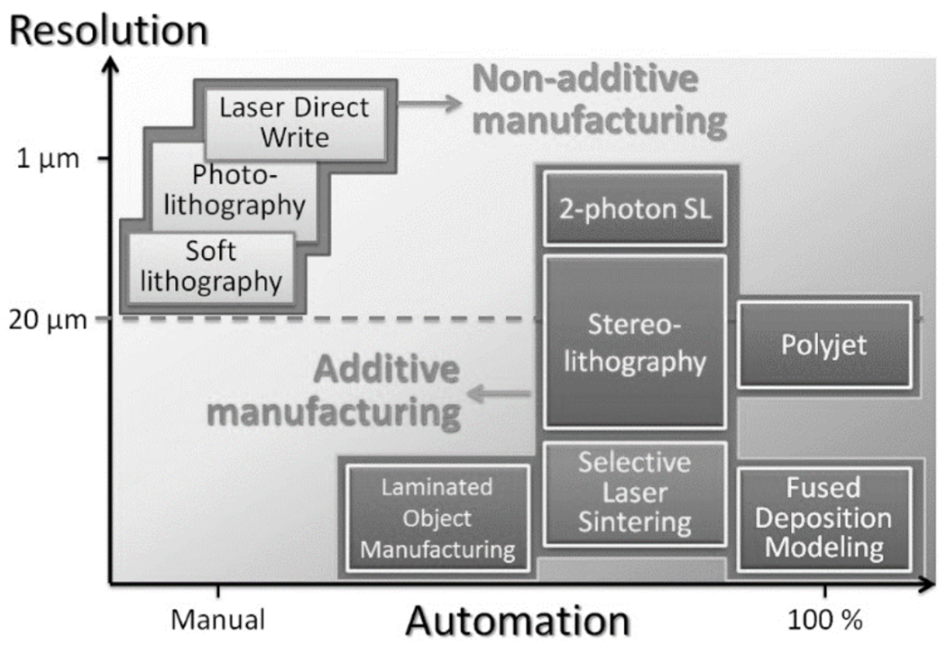
Resolution and automation trade-off in the transition from non-additive to additive manufacturing.
4. Salient Features of Stereolithography Compared to PDMS and Plastic Molding
Traditionally, SL has been perceived by many microfabrication researchers as being inferior to soft lithography in many key aspects (Figure 11), but opinion is quickly changing. Soft lithography, as commonly discussed, benefits from the high resolution of the molds produced by photolithography and the high biocompatibility of PDMS, but suffers from low throughputs and unreliable assembly and bonding processes, resulting in layered designs of poor user-friendliness. SL has a set of features that almost mirror in reverse those of PDMS: SL benefits from full-digital design of 3D architectures and from automated fabrication (which enables fabrication by service bureaus), but the resolution of standard SL machines is inferior to PDMS molding and most SL resins are not biocompatible. Previously, we estimated that the cost of ordering a single SL-printed device from a service bureau is roughly equivalent to the cost of fabricating an SU-8 master mold[12]. On a commercial SL machine, devices covering a build area of 125 mm x 125 mm or larger may be printed in under 10 hours.
Figure 11.
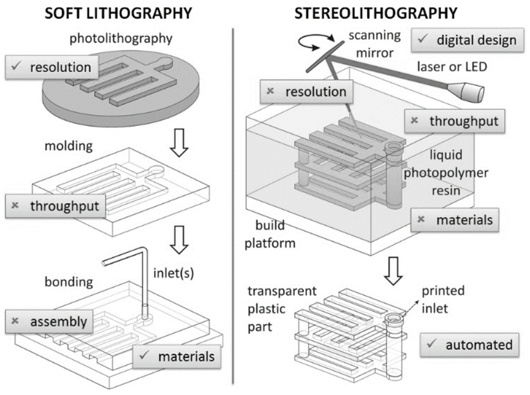
A conceptual overview of the features of merit (√) and disadvantages (×) of soft lithography and stereolithography as traditionally perceived by researchers.
4.1. 3D Capability
PDMS and molded plastic microfluidic devices must be built by stacking layers, and the layers must be bonded together (e.g., see Ref. [83]). This process severely restricts the structures, the connectivity, and the functionality of the devices that can be built. SL is essentially an assembly-free digital manufacturing technique, so manufacturing complexity and manufacturing variety come at no cost; the functionality or connectivity of a given part has only dimensional restrictions (the part has to be built larger than the machine’s resolution) but has few topological restrictions, which creates opportunities for design innovation. (Note that, when printing with a single material, the need for digital slicing and printing in the presence of gravity prohibits the printing of “floating objects” – for example, an unsupported sphere must be tethered.) In some embodiments of SL, it is possible to build parts in more than one material[84] (i.e., two-material parts that have varying materials properties; see below), which offers an even richer spectrum of design possibilities.
4.2. Resolution and Throughput
At present, the “3D freedom” afforded by single-photon SL comes at the cost of lower resolution compared to PDMS/plastic-based devices. The high cost of two-photon laser setups still impedes their wide dissemination in the consumer market, so multi-photon systems remain largely academic[57–58]. All SL desktop systems use single-photon optics (laser or LED source). A quick survey of the available SL services shows that they can build (closed) microchannels that typically measure 500 μm × 500 μm or larger in cross section, although the machines can fabricate smaller open-surface features (e.g., open trenches). In other words, the limitation is not the optics. Thus the main (legitimate) concern of microfluidic users is that the resolution of SL is lower than the resolution they are used to working with. Like soft lithography, SL is perceived as suffering from poor throughputs. However, recent developments in SL technology demonstrate critical improvements in printing speed and resolution. The year 2014, with the expiration of key SL patents, saw the appearance of many companies rushing to innovate; in the span of a few months at the beginning of 2015, Ilios announced a printer with 25 μm XY resolution (6 μm Z layers) and capable of four-material prints[85], Old World Labs announced another printer with <1 μm XYZ resolution[86], and Carbon3D announced a printer capable of printing in minutes instead of hours (~100x faster) with 1 μm XYZ resolution[37]. Clearly, industry is now leading the innovation in resolution and throughput. Systems with <5 μm-resolution for <$10K in less than one year are not far-fetched. However, the biocompatibility of the resins is still a concern and will be discussed in a later section.
4.3. MicroChannel Drainage: Limitations in Resolution and in Automated Fabrication
Even though laser light scattering and diffusion of polymer precursors both impose fundamental limits on the resolution in SL, in practice, the resolution of closed channels depends on the drainage of the liquid polymer precursor that is trapped inside after a device is finished printing. For long channels, this “hydrodynamic limitation” can be more important than the limitation imposed by the photoreaction. Unfortunately, this subtlety is not well appreciated by most printing services. To improve resolution and to facilitate the drainage of otherwise dead-end features, an efficient strategy can be to incorporate drain structures (e.g., shortcut holes, channels and/or temporary “breakable” connectors) that reduce the hydrodynamic resistance of the resin’s exit path. An example of shortcut holes is shown in Figure 12. The newer generation of less viscous photopolymer resins will also facilitate drainage.
Figure 12.
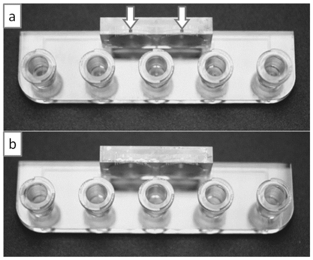
Implementation of drainage holes to simplify device architecture. (a) In this device the channels are fabricated with a square 635 μm x 635 μm outlet hole (indicated by arrows) so that the resin can be easily drained to the exterior. (b) The drainage holes can be sealed with adhesive tape or with epoxy. Reproduced from Ref. [87] with permission of The Royal Society of Chemistry.
The need for microchannel drainage at the end of the fabrication process leads to another important implication – it is a manual process that requires some preparations and it only permits automation for a given inlet layout. Therefore, a) strictly speaking, SL, as applied to microfluidics, should be described as a quasi-automated, quasi-additive fabrication process (some post-processing and resin removal is necessary); b) drainage results in additional setup time and post-fabrication handling that cannot be overlooked, especially for high-volume applications; c) drainage requires the use of (small amounts of) solvents, which adds disposal costs, and some equipment for powering the fluids, which incurs some capital cost.
4.4. Materials Considerations
Understandably, most microfluidic researchers – including our group – have fallen under the “spell” of PDMS for many years due to the optimal properties of PDMS: PDMS is inexpensive, optically clear, elastomeric, biocompatible, and can be molded using methods that can be safely used even by kindergarteners. SL resins, on the other hand, have historically been costly, yellowish at best, and of questionable biocompatibility that has rarely been studied. Not surprisingly, most biomedical researchers have been reluctant to use them. However, the last few years have seen a great deal of innovation in this area.
4.4.1. Biocompatibility
There exist now a number of choices of biocompatible resins. One of the most notable ones is a UV resin produced by DSM (Heerlen, Netherlands) under the trade name Somos Watershed XC 11122. After printing, the cured Watershed is rinsed with isopropyl alcohol and flood-exposed to UV. At the end of this processing, Watershed is nearly colorless with a clarity, flexibility and hardness similar to polycarbonate or poly(methyl methacrylate). (Prolonged exposure of Watershed to UV gives it a yellowish tint.) Furthermore, it does not swell in water and meets biocompatibility standards ISO 10993-5 (Cytotoxicity), ISO 10993-10 (Sensitization), ISO 10993-10 (Irritation), and USP Class VI. We have studied the cytocompatibility of 24-hr C2C12 myoblast cell cultures on Matrigel-coated WaterShed for 24 h and found no noticeable difference when compared to cells cultured on Matrigel-coated tissue culture polystyrene (Figure 13a,b). Longer term cytocompatibility on WaterShed awaits further investigation.
Figure 13.

Biocompatibility of SL prints. (a) C2C12 cells cultured on tissue culture polystyrene (TCPS) control surfaces coated with Matrigel; the cells have been stained for viability with Live/Dead cell stain after 1 day in culture. (b) C2C12 cells cultured on WaterShed surfaces coated with Matrigel using the same seeding and coating protocols as in (a); cell viability on WaterShed surfaces is indistinguishable from that on tissue culture polystyrene surfaces. (c) SEM of hollow microneedles fabricated in e-shell 200 by DLP SL. (d & e) SEM of microneedles fabricated in Ormocer by DLW. Panels (a) and (b) are reproduced from Ref. [87] with permission of The Royal Society of Chemistry. Panel (c) is reprinted from Ref. [88] with permission. Copyright 2011, AIP Publishing LLC. Panels (d) and (e) are reproduced from Ref. [89] with permission of John Wiley and Sons.
Additional biocompatibility data can be found in the drug delivery field, which has investigated the use of SL for the fabrication of implantable microneedles for more than a decade now. Matsuda and Mizutani produced microneedles with a custom acrylate resin containing polycaprolactone[90]; loading of the microneedles with the anti-inflammatory drug indomethacin suppressed the foreign-body inflammatory reaction caused by the needles. Narayan’s group has used e-Shell 200 and 300, commercially-available acrylate-based polymers, to fabricate microneedles by SL[88] and DLW[91] (Figure 13c); these materials, which have been used to manufacture hearing aids, are water-resistant and Class IIa biocompatible. The same group has developed very sharp ceramic-like tips in Ormocer[89, 92] (Figure 13d,e), a material that has been used to produce high-resolution structures including 50 μm-wide channels[93]. These microneedles penetrated cadaveric porcine adipose tissue without fracture and Ormocer surfaces supported the culture of human epidermal keratinocytes for 3 days without significant reduction in viability compared to control surfaces.
Some SL systems have demonstrated successful combination of photocrosslinkable hydrogels and cells. PEG-diacrylate[48–49], gelatin methacrylate[50], hyaluronic acid[51], and PEGylated/functionalized alginates[52], all highly biocompatible matrices, have been used to print cells encapsulated in hydrogel (see Figure 4) – which is derivatized with adhesive ECM proteins or cell-attachment peptide sequences. Cells used in these studies have included fibroblasts[49a], neurons, muscles cells[52], and human mesenchymal stem cells[94]. These hydrogels have been envisioned to constitute parts of bioactuators and bio-sensors that incorporate live cells[53]. Stampfl et al.[93] screened a number of acrylate-based monomers, combined with diluents (water or PEG 400 M.W.) and the photoinitiator Irgacure 819 to produce various hydrogel resins with a range of mechanical properties (with a Young’s Modulus from 0.4 to 8000 MPa) which they compared to those of the commercially-available resins Ormocer and Renshape. As soon as SL materials research moves to optimize materials for biomedical applications, we should see the birth of a new variety of SL resins that are biocompatible (even implantable and/or bioresorbable), transparent, and gas-permeable.
4.4.2. PEG-DA, the ideal candidate
The field of cell encapsulation provides us with a great example of a photopolymerizable, biocompatible material: PEG-diacrylate (PEG-DA), which as a hydrogel has been used extensively to trap cells and create 3D tissue constructs[48–49, 95]. Photopolymerization schemes require a photoinitiator, a chemical compound that decomposes into free radicals or cations when exposed to light. Photoinitiators differ in their cytotoxicity, solubility in water, and stability. Intense efforts have been spent in developing and evaluating cytocompatible photoinitiators[96]. Irgacure 2959 photoinitiator (Ciba) is frequently used with 325 nm light and can be utilized to encapsulate delicate cells such as stem cells with high viability[97]. The main challenge has been to find a biocompatible photoinitiator that works for light sources of the new generation of “desktop” SL systems (λ = 405 nm ”near UV” visible light, which is more benign to cells). For 405 nm, Irgacure 784 is available but is water-insoluble (must be dissolved in DMSO). Alternatively, lithium phenyl-2,4,6-trimethylbenzoylphosphinate (LAP, only recently commercially-available) is water-soluble and very cytocompatible[98]. LAP has been recently re-discovered by Kristi Anseth’s group as a water-soluble type I photoinitiator that is uniquely active in the visible range (λ = 405 nm and above)[98–99]. This initiator has been shown to be cytocompatible, and has proved suitable for cell encapsulation studies with PEG-DA[98, 100]. It is important to stress that while the issue of the cytocompability of the photoinitiator should not be as relevant to building microfluidic devices as it is for encapsulating cells, it is desirable that photoinitiator molecules potentially leeching from the device walls be as cytocompatible as possible.
There is abundant evidence that PEG-DA is a very suitable material for microfluidics. Khademhosseini and Suh fabricated PEG-DA microchannels (by photolithography) and demonstrated that, when using low molecular weight, heavily-crosslinked PEG-DA (MW = 258), the channels resisted swelling (and were impermeable to water) for up to 2 weeks, whereas higher-MW PEG-DA (MW = 875) showed significant swelling and collapse of the channels within 5 hours[101]. Woolley’s group has demonstrated PEG-DA microfluidic valves (by molding and layering)[102] and made an exhaustive evaluation of the various favorable properties of PEG-DA compared to glass, PDMS, and other polymers[103]. Thus PEG-DA seems an ideal resin for 3D-printable biomedical devices.
4.4.3. Solvent Compatibility
PDMS is a very porous matrix that swells in organic solvents, which results in loss of solvent into the microchannel walls, detachment of the seal between the channels and the surface, and alteration of the channel geometries [6]. For this reason, many microfluidics research efforts have been directed towards developing polymer matrices that do not swell, especially microvalves whose flexural element is made of Viton[104] or Teflon[105] in a chemically-resistant microchannel seat.
Research into SL resins has produced a variety of resins with a wide range of properties. Somos 9920, for example, is a durable resin whose properties mimic polypropylene, offering great chemical resistance. (Polypropylene is used to store solvents.) Somos 5530HT is also rated as solvent-resistant, water-resistant, and highly temperature resistant. Somos 11120 (also termed “WaterShed”) is highly resistant to water (but not organic solvents), transparent, and mechanically very strong.
4.4.4. Wettability
Modulation of the wetting properties of SL resins is of paramount importance in microfluidics, since bubbles can form during filling and can be difficult to dislodge. SL-printed plastics do not have the high gas solubility of PDMS (which obeys Henry’s law; i.e., the equilibrium concentration of gas dissolved in PDMS is proportional to the partial pressure of gas present in the PDMS channels[106]), so the convenient trick for dislodging bubbles from PDMS devices by pressurization of the fluids (which causes the bubbles to disappear into the PDMS walls) does not work in SL-printed plastic devices. Yang and co-workers added a vinyl-terminated initiator into the resin base (containing acrylate-based pre-polymers) to produce poly(ethylene glycol) methacrylate (PEGMA), a very hydrophilic and biocompatible polymer (which facilitated spontaneous filling, contact angle ~40°), or perfluorodecyl methacrylate (PFMA), a very hydrophobic polymer (contact angle ~123°)[107] (Figure 14a,b); hydrophobic coatings can be used to create aqueous partitions inside these devices.
Figure 14.
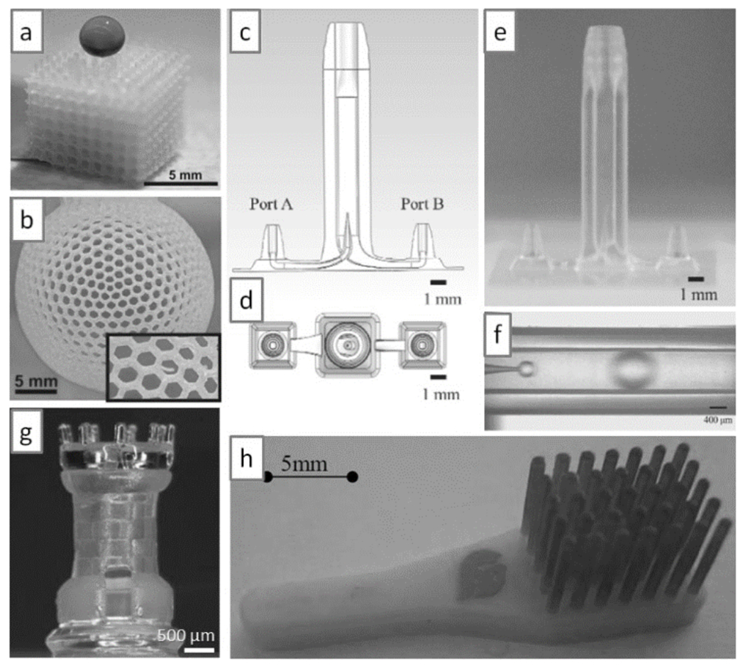
Multi-material SL printing. (a) SL-printed cube in a super-hydrophobic resin; note that a droplet of dye deposited on the cube does not penetrate the cube. (b) SL-printed sphere in a super-hydrophobic resin; the sphere is filled with dye, yet it does not leak through its 1 mm-side hexagonal holes (see inset). (c & d) Schematic side and top view, respectively, of a droplet generator. (e) SL print of the device in (c); the inner channel has an internal diameter of 50 μm and the fabrication accuracy is ~5 μm. (f) Droplet generation in the SL-printed device shown in (e). (g) A 3-material SL print; the chess piece has internal structures. (h) A two-material SL print; the red tips are printed in an elastomeric resin. Panel (a) and (b) are reproduced from Ref. [107] with permission of The Royal Society of Chemistry. Panels (c) to (f) are reproduced from Ref. [110] with permission of the Japan Oil Chemists’ Society. Panel (g) is reproduced from Ref. [84a] with permission of Springer Science and Business Media. Panel (h) is reproduced from Ref. [84b] with permission of the authors.
4.4.5. Surface Derivatization and Bonding
Surface derivatization of printed SL resins has been achieved with commercially-available silanes[108]. The compound 3-glycidoxypropyltrimethoxysilane (GPTMS, purchased from Sigma Aldrich, Germany) was used to create a siloxane layer on the surface of an epoxy-based resin under acidic conditions in the presence of a photoacid generator, triarylsulfonium hexafluoroantimonate (TASHFA, purchased from Sigma Aldrich), and UV light exposure. This chemistry was used to bond slabs of PDMS to the SL-printed resin. Epoxy slides have been used to chemically immobilize protein surface gradients via amine-epoxy linkage for chemotaxis experiments[109], so in principle epoxy-based SL resins could be utilized to print chemotaxis devices. Another option is to derivatize the walls of the channel with a silicate coating, which produces a surface that is amenable to standard silane chemistry. Ohtani et al.[110] injected a hydrolyzed ethyl silicate solution (N-103X, Colcoat Co.) into the channel (part of a droplet generator[111], see Figure 14c–e), then heated the device to 120°C for 30 min to vaporize the solvent and cure the coating on the walls. After the hydrophilic treatment, the silicate surface was derivatized with a fluorosilane compound to render it hydrophobic, which enabled the treated device to produce monodisperse inverted water-in-oil emulsions (Figure 14f). Silane derivatization could enable silicate-like coatings made of allylhydridopolycarbosilane that confer polymer surfaces an electrophoretic mobility and a solvent resistance that (while retaining transparency) is indistinguishable from that of glass over at least 90 days[112]. We have found that WaterShed XC 11122 resin bonds to O2 plasma-activated surfaces such as glass, polystyrene, or PDMS, provided the surfaces are heated above the glass-transition temperature of the resin (~42.5°C)[113]. This simple procedure circumvents the TASHFA and UV illumination steps described above.
4.4.6. Multi-Material Stereolithography Printing
Although SL is traditionally regarded as a technique limited to printing in a single polymer material, recent advances in resins and SL printers have pushed the frontiers into multiple-material printing[84] (Figure 14g), including elastomers[84b] (Figure 14h) and ceramics[114]. Cho’s group observed that when they added copper microparticles to a photoresin, a sintering process rendered the microstructures conductive (resistivity ~10 times that of pure copper) with a shrinkage of 22-28%[115]. We can now foresee sensors and actuators containing parts that are flexible and/or metallic[116]. A new generation of multi-material printers[85] could allow for the creation of polymer gradients with new, interesting properties and for the printing of multi-material sensors and actuators.
4.5. Digital Inspection and Finite-Element Modeling Prior to Fabrication
One of the biggest advantages of SL (and 3D-printing in general) is the ability to fully predict the performance of a device prior to printing it. The design can be sent via email and digitally inspected by a team of experts that is in a remote location with respect to the design team. The inspection report can be returned in the form of a written email, a Skype teleconference call, or amendments to the CAD design file. Inspection need not be limited to visualizing and correcting the architecture of the device. A researcher can now use finite-element modeling software to virtually test the expected mechanical performance such as the flexural bending or the resonance frequency of a critical component, or use fluid dynamics simulation software to test the performance of a mixer design – or both (in the case of a microvalve). Once the design “works” in the simulator, then it can be printed. We predict that in the near future, this rational “CAD approach” to microfluidics will save an enormous amount of time and resources for complex projects.
4.6. Overcoming the Barriers to Device Dissemination with 3D-Printing
4.6.1. From Cumbersome PDMS Inlets to Intuitive 3D-Printed Modular Architectures that Incorporate Industry-Standard User Interfaces
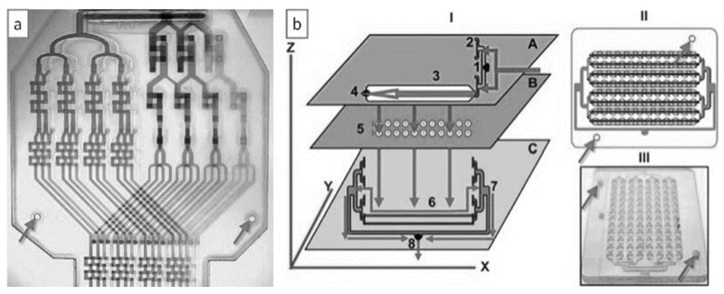
Although microfluidics is now a mature field[1], in the last 30 years, the soft lithography community has not been able to agree on a simple standard of tubing and inlet/outlet connectors. A device with 16 input fluid lines and 20 control pneumatic lines as shown in Figure 1[83a] can be daunting to interface with. Part of the problem is due to the economics of how we do research: we are rewarded for proof-of-concept, not for sleek devices; punching inlets in PDMS has worked fine until now. As society and the funding agencies push for research to be translated into products, however, user-friendliness has suddenly taken center stage. We believe that 3D-printing will rapidly engage the community into adopting connector and inlet modules that are already existing industry standards.
Modular design is an inherent part of 3D-printing. With 3D-printing, the microfluidic designer has no other choice but to fully specify the packaging (interface, connectors, etc.) in CAD software prior to printing. SL-printed plastic 3D circuits with packaged connectors can be built as interlocking modules and trivially operated[117] (Figure 15a,b). Importantly, a robust, reliable mixer could be built from assembling various modules[117c], dispelling the popular notion that such modular systems tend to disrupt flow and increase user error and dead volume. It might be argued that post-fabrication assembly of the modules is not an effective strategy because it does not use the full capabilities of SL (being an assembly-free fabrication technique); indeed, in some instances assembly of the modules may require metal pins or O-rings to prevent leakage[117d]. In any case, the concept of “modular design” can be extended beyond physical modules to produce designs by Joining various digital modules. An eloquent call for modularity in the design of microfluidic systems was made in the field of droplet engineering[118]. Medical-grade (industry-standard) connectors such as Luer Lock or barb-type connectors can be imported from a free repository and copied/pasted into the CAD design before printing[12] (Figure 15c), resulting in devices that are more user-friendly than their PDMS or plastic-molded cousins. Importantly, digital designs can be inspected and improved upon by another group or groups before printing. We predict that teams formed by mechanical engineers, industrial designers and interaction/experience designers will increasingly contribute to microfluidics and improve the functionality of devices. Bioreactors for bacterial culture[119] (Figure 15d) and microfluidic mixers printed with a desktop printer[120] (Figure 15e,f) are Just examples of what is coming. While most PDMS and plastic chips serve as simple “flat containers” for the fluidic architecture of the chip – making sample introduction problematic, with 3D-printing, introduction of the sample can be shifted to more intuitive paradigms including boxes or lids that can be opened and closed with hinges, latches, springs, notches, and belts. This new paradigm will facilitate the design of chips made of multiple materials, for example a saliva or blood sample could be contained on a piece of paper and the user would only need to deposit it inside a closeable box.
Figure 15.
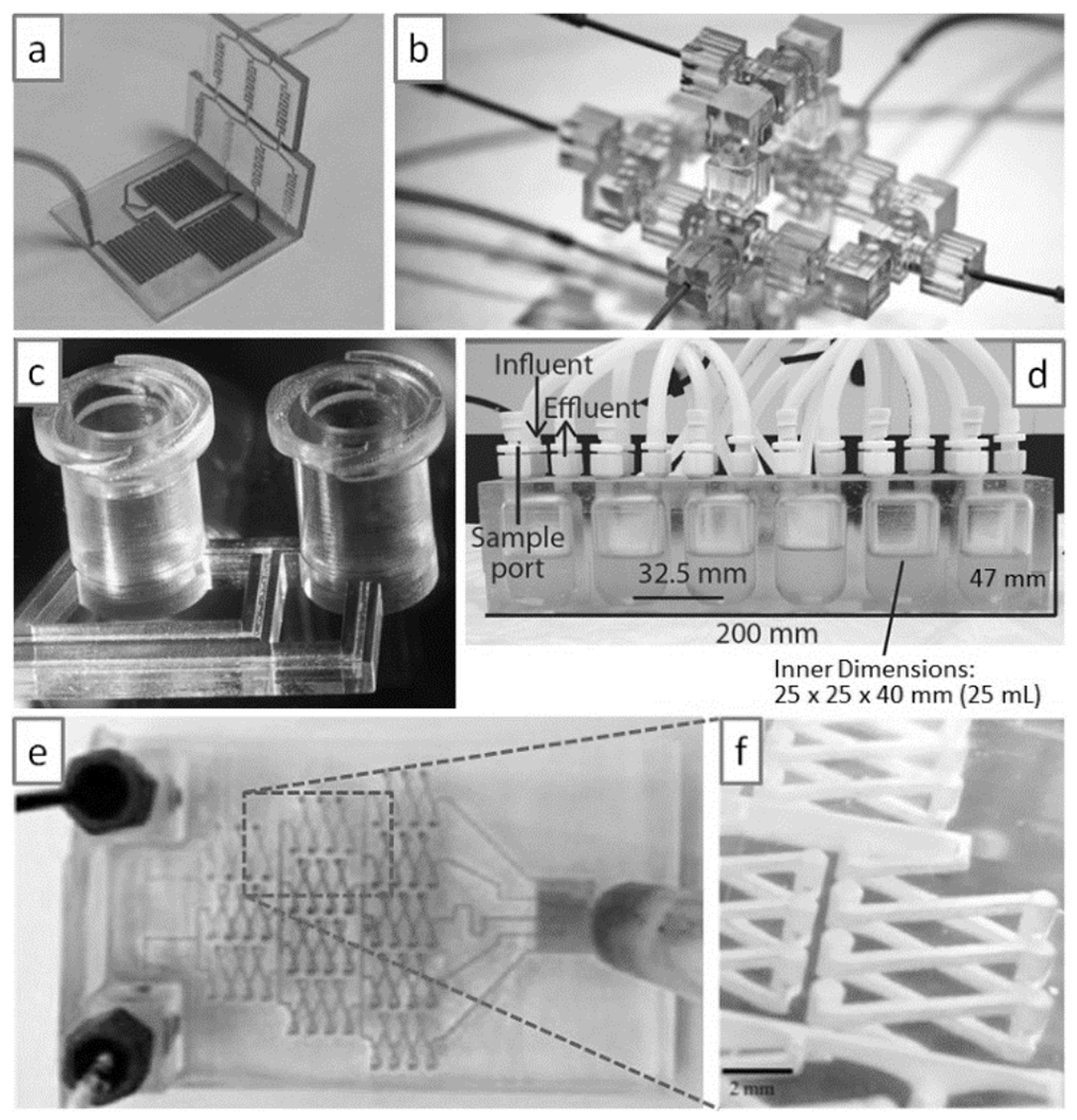
Modular microfluidics. (a) A modular mixer built by SL. (b) A modular droplet generator built by SL. (c) Example of user-friendly connectivity (here, an industry-standard Luer-Lock connector printed by SL). (d) Complex bioreactor printed by SL. (e & f) A complex mixer printed with a commercial desktop SL system. Panel (a) is reproduced from Ref. [117b] with permission of The Royal Society of Chemistry. Panel (b) is reproduced from Ref. [117c]. Copyright 2014 National Academy of Sciences, USA. Panel (c) is reproduced from Ref. [12] with permission of The Royal Society of Chemistry. Panel (d) is reproduced from Ref. [119] with permission of American Society for Microbiology. Panels (e) and (f) are reproduced from Ref. [120] with permission. Copyright 2014 American Chemical Society.
We envision a future dominated by SL printing where microfluidic designs will be available online, and it will be possible to download them and integrate them as modules that will be connected to other devices, modules, or packagings. It seems obvious that, using digital design tools, SL packagings used by the microfluidics community will soon converge towards user-friendly interfaces that will incorporate existing biomedical-standard connectors. Thus, we believe that the biggest impact that 3D-printing technology will have in microfluidics will not be so much in the incorporation of “3D piping” but in the introduction of modular design paradigms that will amplify the efforts of individual teams.
4.6.2. From PDMS Multi-Layer Valves to 3D-Printable Valves
Fluid handling is a ubiquitous and often tedious operation in biomedicine, from benchtop research that uses cell culture media to clinical diagnostics that use bodily fluids. Most often, fluids are transferred from container to container by means of pipettors that are operated by humans (a tedious and costly mode of operation that is prone to error) or by expensive robotic dispensers. Valves and pumps are essential for automating fluid handling; automation reduces human labor costs, speeds processing, and enables mass parallelization. The advent of PDMS microvalves and micropumps[5a, 5c], for example, revolutionized the field of microfluidics and allowed for the miniaturization and automation of a vast array of biomedical assays[121]. All-plastic microvalves (to improve upon the solvent incompatibilities of PDMS) have been developed[104–105, 122]. However, present fabrication of valves and pumps is expensive because it consists of multiple steps, including molding, machining, bonding, and/or assembly of small parts.
The Folch lab has invented diaphragm valves and peristaltic pumps that can be 3D-printed by SL[113] (Figure 16). A valve in operation is shown in Figure 16b,c. The diaphragm is a 10 mm-diam., 100 μm-thick plastic membrane that is integrally printed inside a chamber and that can be pneumatically deflected by pressurization of the control line (Figure 16d,e). 3D-printable valves and pumps can be downloaded as digital objects and incorporated modularly into other devices. Two valves can be used to build a switch (Figure 16f), and three valves can be put together in series to build a peristaltic pump (Figure 16g). No appreciable valve leakage was measured in the closed-valve state, even though the membrane is not built of a self-sealing material (e.g., PDMS). Valve closing pressures were reproducible over many valve closing cycles. The valve’s fluidic resistance exhibits a sigmoidal response to control pressure; this multi-state valving behavior could find applications in microfluidic multiplexers[123], flow regulators[124], and fluidic amplifiers[125]. 3D-printable valves and pumps can be used to replace costly human labor and robotic pipettors and can be inexpensively printed in transparent biocompatible plastics from any computer, anywhere in the world. Improvements in the 3D-printing process (resolution, materials, etc.) will be required before the valves can be further miniaturized.
Figure 16.
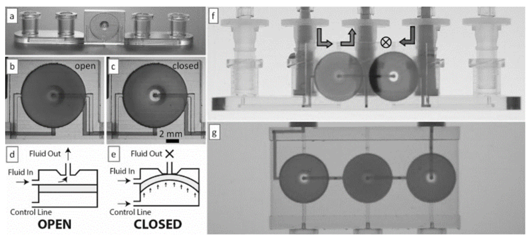
3D-printed valves, switches and pumps. (a) Photograph of a single-valve device 3D-printed in WaterShed XC 11122 resin. (b & c) Micrographs showing the dye-filled valve in its open (b) and closed (c) states. (d & e) Side-view schematics depicting a valve in its open (d) and closed (e) states. (f) Photograph of a switching device selecting for solution passing through the valve on the left. (g) A peristaltic pump during an actuation phase in which only the middle valve is open. Panels (a) through (g) are reproduced from Ref. [87] with permission of The Royal Society of Chemistry.
4.6.3. From Bulky Control Systems to Autonomous Microfluidics Using Embedded 3D-Printed Controls
While the above 3D-printed systems are still tethered to bulky control systems requiring computers and electrical signals, work is underway to incorporate 3D-printed automation. The Ismagilov lab has 3D-printed a clever “pumping lid” that pressurizes (or pulls vacuum from) the inlet(s) of a microfluidic device[64] (Figure 17). The lid is made of two materials and is fabricated by photopolymer inkjet printing; an elastomeric gasket ensures that the lid seals properly to the inlet(s). This simple system altogether eliminates the need for external power in driving microfluidic flow for most applications (the pump lasts for >2 hours).
Figure 17.
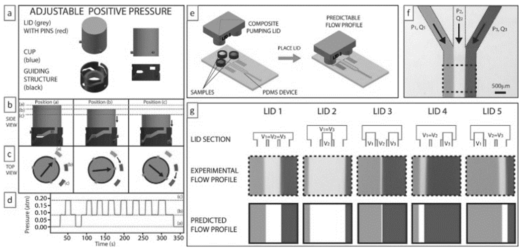
3D-printed “pumping lid”. (a) The “pumping lid” (grey) produces a positive pressure by turning down on a guiding structure that contains a soft elastomeric cup. (b & c) The lid can lock at various (“a/b/c”) positions (indicated in dotted lines or rectangles), each of which produces different pressures. (d) Experimental pressure profile obtained by turning the lid between the three positions. A similar design can generate negative pressures. (e) Schematic of a three-cup composite pumping lid for producing three different pressures in the same device. (f) Micrograph of the Junction at which three channels combine to produce a heterogeneous laminar flow. (g) Different composite lids (top row schematics) can be used to produce different flow profiles (middle row) that agree very well with the predictions of the flow profiles (bottom row) based on the pressures produced by the lids and the device geometry. Reproduced from Ref. [64] with permission of The Royal Society of Chemistry.
3D-printed valves could also simplify the fabrication of microfluidic logic elements, such as adding machines[10a], memory latches[10b], shift-registers[10c], autonomous pumps[10d] and oscillators[10e, 10f]. We can envision 3D-printed, truly autonomous microfluidic machines with embedded controls (powered by flow or a manually-generated pressure differential) that can run pre-programmed biochemical and cell-based assays without the use of pneumatics, electricity, or tubing.
4.6.4. Designs Can Be Disseminated and Sold via the Web
3D-printing minimizes the barriers to manufacturing. Most microfluidic devices are made by PDMS molding or glass etching because these two techniques are low-cost, prototyping techniques that are convenient to the operation and budgets of academic laboratories. Unfortunately, neither PDMS molding nor glass etching allow for large-volume manufacturing, a condition needed for most companies to recover their big initial investments.
Engineers are designers, but so far they have not had the tools to monetize the products of their research with sufficient agility. MakerBot has already created a very vibrant website (called “Thingiverse”[67]) for sharing CAD designs, however only designs with non-commercial (Creative Commons[126]) licenses are allowed. Note that in the traditional model of device commercialization, engineers design several prototype iterations until a final prototype is ready for commercial launch. In academia, the various iterations have monetary value to other designers working in a similar field. Based on this simple principle, the company 3DSkema will soon launch an online marketplace where designers can submit their licensed designs and offer them for sale (or for share with a non-commercial license). This model radically departs from previous commercialization models in that inventors are allowed to monetize their various prototypes without proceeding through the costly patent/plastic product route.
5. Summary and Outlook
It has been argued that microfluidics produces very few “killer applications”[1, 127], in the sense that it is difficult for microfluidic products to reach the consumer market. Here we argue that there is no lack of “killer apps” – it is the commercialization pipeline that is obstructed. We have seen that this obstruction is due to at least three main causes: a) user interfaces have not reached a standardization point; b) microfluidic systems still rely on complex control systems; and c) PDMS-molding processes are not easily commercialized. 3D-printing appears to be a suitable technology to address these key points. Still, the application of 3D-printing (and in particular SL) to microfluidics is in its infancy. Historically, soft lithography came to dominate the microfluidics turf previously occupied by silicon and glass micromachining because PDMS-molded prototypes were cheaper and faster to produce, were more biocompatible and transparent, and could incorporate microvalves and micropumps – all despite obvious losses in resolution. However, PDMS microchannels cannot be made with arbitrary aspect ratios, and PDMS flexibility can be a severe problem for alignment of multiple layers. The transition from soft lithography to 3D-printing is already being marked by a similar set of constraints that can be turned into opportunities:
1). Cost vs. resolution:
DLW/two-photon SL machines – which are prohibitively expensive and thus their applications have reduced impact – are capable of printing 10 μm-wide channels and ~1 μm-resolution surface features. Several key SL patents have expired in 2014; as a result, there have been a proliferation of new commercial desktop SL printers, and their prices have dropped to an average of less than $5,000. These affordable desktop single-photon SL machines can fabricate features down to 25 μm[85], and smaller (~1 μm) features are expected with newer machines[37, 86] and lower-viscosity resins. A microfluidic device SL-printed by a mail-order service is now already cheaper than a similar device fabricated in PDMS when all factors (materials, salary, time) are taken into account, so the devices that will be printed 5 years from now should be cheaper and more architecturally complex than the PDMS devices that are being molded today.
2). Materials development:
Most microfluidic engineers are reluctant to use SL (and other 3D-printing techniques) because of concerns surrounding the biocompatibility of the resins. However, it should be understood that the use of many SL resins is being artificially incentivized for commercial reasons by their developers. Of less interest to commercial developers, some of the most promising resins from a biomedical perspective (e.g., PEG-DA) are inexpensive and patent-free, as they were developed a long time ago to develop biomaterials (photocrosslinkable hydrogels) for cell encapsulation. While PDMS does not allow for keeping cells alive or for diffusing large molecules within its matrix, in the next years, as the SL microfluidics community grows, it is to be expected that researchers will produce materials optimized for bio-microfluidic fabrication, including bio-resorbable and gas-porous matrices. New developments in automated multi-material printing will also have a big impact on sensors and actuators.
3). Computer-aided design (CAD).
3D-printing device design, unlike soft lithography, is inherently computer-aided and amenable to digital modules, which benefits user-friendly packaging, the use of performance simulation tools, and the electronic dissemination and monetization of the designs. This feature alone is expected to revolutionize the field of microfluidics.
4). Fluid automation:
We and others have invented 3D-printable elements that are essential for automated fluid handling in microchannels, such as valves and pumps. 3D-printable valves and pumps can be downloaded as digital objects and incorporated modularly into other devices; they can be inexpensively printed in transparent biocompatible plastics from any computer, anywhere in the world; and they can be used to replace costly human labor and robotic pipettors.
In summary, additive manufacturing techniques represent a “3D-printing revolution” because they are economically efficient to an extreme: they favor modular and team-based CAD, require neither tooling nor assembly, produce minimal waste, and minimize distribution costs. If (and only if) a large-enough capital investment can be safely invested to run a large-enough production, then a high-throughput fabrication technique such as injection molding is sure to provide the lowest cost per device. Otherwise, for low to mid-scale production, despite being based on low-throughput serial fabrication, the economics usually favor 3D-printing techniques against high-throughput molding techniques when all factors are considered. Indeed, the ability to rapidly prototype a physical model in a few hours has already revolutionized the product design process by allowing designers to test designs before investing in tooling or fabrication processes. In biomedicine, shortening the time from prototype to product should enable personalized devices and treatments, accelerate R&D, and help reduce the cost of clinical trials and of the overall access to healthcare.
Biographies
Anthony Au obtained his B.S. in Biomedical Engineering at Johns Hopkins University in 2008 and his Ph.D. in Bioengineering at the University of Washington in 2014 under the direction of Prof. Albert Folch. He previously worked as an engineer at a biotech startup and as a research assistant at biotech companies and academic institutions. He is currently working on the development and manufacturing of wearable electronic devices for the diagnosis, monitoring, and treatment of specific medical conditions.

Wilson Huynh obtained his B.S. in Bioengineering at the University of Washington in 2014. As an undergraduate, he worked as a research assistant under the mentorship of Prof. Albert Folch. His research involved the development of user-friendly microfluidic devices for drug screening and personalized cancer therapies. He is currently working as a clinical assistant at a cancer research center in Seattle, Washington, where he is investigating the impacts of current cancer treatment modalities on patients

Lisa Horowitz obtained her M.D. and Ph.D. in Neuroscience at Harvard Medical School under Prof. Linda Buck in 2000. She continued with postdoctoral studies on ion channel modulation with Bertil Hille at the University of Washington, before returning to work on olfaction with Linda Buck at the Fred Hutchinson Cancer Research Center. Since, she has worked on the interface of microfluidics and biology, including projects involving neuroscience, immunotherapy, and cancer treatment with Daniel Storm, Michael Jensen, Albert Folch, and Robert Rostomily.

Albert Folch obtained his Ph.D. in Nanotechnology from the University of Barcelona in 1994. He was a postdoc at MIT under Martin Schmidt and Mark Wrighton, and at Harvard under Mehmet Toner. He has been at the University of Washington since 2000 where he is an Associate Professor in Bioengineering, and he is the author of four books, including “Introduction to BioMEMS”. His lab works at the interface between microfluidics, neurobiology and cancer. Since 2007, his lab has run a celebrated outreach art program called BAIT (Bringing Art Into Technology).

References
- [1].Whitesides GM, Nature 2006, 442, 368. [DOI] [PubMed] [Google Scholar]
- [2].a) Dittrich PS, Manz A, Nature Rev Drug Disc 2006, 5, 210; [DOI] [PubMed] [Google Scholar]; b) El-Ali J, Sorger PK, Jensen KF, Nature 2006, 442, 403. [DOI] [PubMed] [Google Scholar]
- [3].Sackmann EK, Fulton AL, Beebe DJ, Nature 2014, 507, 181. [DOI] [PubMed] [Google Scholar]
- [4].Xia YN, Whitesides GM, Angew. Chem.-Int. Edit. Engl 1998, 37, 551. [Google Scholar]
- [5].a) Unger MA, Chou HP, Thorsen T, Scherer A, Quake SR, Science 2000, 288, 113; [DOI] [PubMed] [Google Scholar]; b) Hosokawa K, Maeda R, J. Micromech. Microeng 2000, 10, 415; [Google Scholar]; c) Thorsen T, Maerkl SJ, Quake SR, Science 2002, 298, 580. [DOI] [PubMed] [Google Scholar]
- [6].Folch A, Introduction to BioMEMS, CRC Press, Boca Raton, FL, 2013. [Google Scholar]
- [7].Sia SK, Whitesides GM, Electrophoresis 2003, 24, 3563. [DOI] [PubMed] [Google Scholar]
- [8].Fuard D, Tzvetkova-Chevolleau T, Decossas S, Tracqui P, Schiavone P, Microelectronic Engineering 2008, 85, 1289. [Google Scholar]
- [9].a) Choi CJ, Cunningham BT, Lab on a Chip 2007, 7, 550; [DOI] [PubMed] [Google Scholar]; b) Chang TC, Mikheev AM, Huynh W, Monnat RJ, Rostomily RC, Folch A, Lab on a Chip 2014, 14, 4540. [DOI] [PMC free article] [PubMed] [Google Scholar]
- [10].a) Jensen EC, Grover WH, Mathies RA, Microelectromechanical Systems, Journal of 2007, 16, 1378; [Google Scholar]; b) Weaver JA, Melin J, Stark D, Quake SR, Horowitz MA, Nat Phys 2010, 6, 218; [Google Scholar]; c) Rhee M, Burns MA, Lab on a Chip 2009, 9, 3131; [DOI] [PMC free article] [PubMed] [Google Scholar]; d) Devaraju NSGK, Unger MA, Lab on a Chip 2012, 12, 4809; [DOI] [PubMed] [Google Scholar]; e) Mosadegh B, Kuo C-H, Tung Y-C, Torisawa Y.-s., Bersano-Begey T, Tavana H, Takayama S, Nat Phys 2010, 6, 433; [DOI] [PMC free article] [PubMed] [Google Scholar]; f) Duncan PN, Nguyen TV, Hui EE, Proceedings of the National Academy of Sciences 2013, 110, 18104. [DOI] [PMC free article] [PubMed] [Google Scholar]
- [11].Ho CM, Ng SH, Li KH, Yoon YJ, Lab Chip 2015, 15, 3627. [DOI] [PubMed] [Google Scholar]
- [12].Au AK, Lee W, Folch A, Lab Chip 2014, 14, 1294. [DOI] [PMC free article] [PubMed] [Google Scholar]
- [13].a) Murr L, Esquivel E, Quinones S, Gaytan S, Lopez M, Martinez E, Medina F, Hernandez D, Martinez E, Martinez J, Stafford S, Brown D, Hoppe T, Meyers W, Lindhe U, Wicker R, Materials characterization 2009, 60, 96; [Google Scholar]; b) Terrazas CA, Gaytan SM, Rodriguez E, Espalin D, Murr LE, Medina F, Wicker RB, Int J Adv Manuf Technol 2013, 71, 33. [Google Scholar]
- [14].a) Mazzoli A, Medical & Biological Engineering & Computing 2013, 51, 245; [DOI] [PubMed] [Google Scholar]; b) Duan B, Wang M, Mrs Bulletin 2011, 36, 998. [Google Scholar]
- [15].Zopf DA, Hollister SJ, Nelson ME, Ohye RG, Green GE, New England Journal of Medicine 2013, 368, 2043. [DOI] [PubMed] [Google Scholar]
- [16].Renishaw.
- [17].Lee MT, Lee D, Sherry A, Grigoropoulos CP, Journal of Micromechanics and Microengineering 2011, 21, 095018. [Google Scholar]
- [18].Pilipovic A, Raos P, Sercer M, International Journal of Advanced Manufacturing Technology 2009, 40, 105. [Google Scholar]
- [19].Ahn DG, Lee JY, Yang DY, Journal of Mechanical Science and Technology 2006, 20, 19. [Google Scholar]
- [20].Cheng YL, Chen SJ, in Progress on Advanced Manufacture for Micro/Nano Technology 2005, Pt 1 and 2, Vol. 505-507 (Eds.: Jywe W, Chen CL, Fan KC, Fung RF, Hanson SG, Hsieh WH, Hsu CL, Huang YM, Hwang YL, Jager G, Jeng YR, Li W, Liao YS, Lin CC, Lin ZC, Sung CK, Tzeng CH), 2006, pp. 1063. [Google Scholar]
- [21].Erbano BO, Opolski AC, Olandoski M, Foggiatto JA, Kubrusly LF, Dietz UA, Zini C, Makita Arantes Marinho MM, Leal AG, Ramina R, Acta Cirurgica Brasileira 2013, 28, 756. [DOI] [PubMed] [Google Scholar]
- [22].Bucella SG, Nava G, Vishunubhatla KC, Caironi M, Organic Electronics 2013, 14, 2249. [Google Scholar]
- [23].S. P. Series.
- [24].Kong YL, Tamargo IA, Kim H, Johnson BN, Gupta MK, Koh T-W, Chin H-A, Steingart DA, Rand BP, McAlpine MC, Nano Letters 2014, 14, 7017. [DOI] [PubMed] [Google Scholar]
- [25].Sun K, Wei T-S, Ahn BY, Seo JY, Dillon SJ, Lewis JA, Advanced Materials 2013, 25, 4539. [DOI] [PubMed] [Google Scholar]
- [26].Muth JT, Vogt DM, Truby RL, Mengüç Y, Kolesky DB, Wood RJ, Lewis JA, Advanced Materials 2014, 26, 6307. [DOI] [PubMed] [Google Scholar]
- [27].Adams JJ, Duoss EB, Malkowski TF, Motala MJ, Ahn BY, Nuzzo RG, Bernhard JT, Lewis JA, Advanced Materials 2011, 23, 1335. [DOI] [PubMed] [Google Scholar]
- [28].Joe Lopes A, MacDonald E, Wicker RB, Rapid Prototyping Journal 2012, 18, 129. [Google Scholar]
- [29].Mannoor MS, Jiang Z, James T, Kong YL, Malatesta KA, Soboyejo WO, Verma N, Gracias DH, McAlpine MC, Nano Letters 2013, 13, 2634. [DOI] [PMC free article] [PubMed] [Google Scholar]
- [30].Bartholomeusz DA, Boutte RW, Andrade JD, Journal of Microelectromechanical Systems 2005, 14, 1364. [Google Scholar]
- [31].a) Himmer T, Nakagawa T, Anzai M, Computers in Industry 1999, 39, 27; [Google Scholar]; b) Obikawa T, Yoshino M, Shinozuka J, Journal of Materials Processing Technology 1999, 90, 171. [Google Scholar]
- [32].Hull C, Mod Cast 1988, 78, 38. [Google Scholar]
- [33].a) Nakamoto T, Yamaguchi K, Abraha PA, Mishima K, Journal of Micromechanics and Microengineering 1996, 6, 240; [Google Scholar]; b) Bertsch A, Bernhard P, Vogt C, Renaud P, Rapid Prototyping Journal 2000, 6, 259. [Google Scholar]
- [34].Waldbaur A, Rapp H, Lange K, Rapp BE, Anal. Meth 2011, 3, 2681. [Google Scholar]
- [35].Bertsch A, Zissi S, Jezequel JY, Corbel S, Andre JC, Micro. Tech 1997, 3, 42. [Google Scholar]
- [36].Pan YY, Zhou C, Chen Y, Journal of Manufacturing Science and Engineering-Transactions of the Asme 2012, 134. [Google Scholar]
- [37].Tumbleston JR, Shirvanyants D, Ermoshkin N, Janusziewicz R, Johnson AR, Kelly D, Chen K, Pinschmidt R, Rolland JP, Ermoshkin A, Samulski ET, DeSimone JM, Science 2015, 347, 1349. [DOI] [PubMed] [Google Scholar]
- [38].a) ; b) G. D. Printers; c) Prism Lab.
- [39].Jonathan W, Martha OW, Paul T, Mallory B, Vaijayantee B, Nicole M, Kyobum K, John PF, Ali S, Yueshuo X, Jean FW, Donald PL, Jiayang S, Arnold IC, David D, Biofabrication 2014, 6, 015003.24429508 [Google Scholar]
- [40].Kawata S, Sun H-B, Tanaka T, Takada K, Nature 2001, 412, 697. [DOI] [PubMed] [Google Scholar]
- [41].I. Nanoscribe.
- [42].Tasoglu S, Demirci U, Trends in Biotechnology 2013, 31, 10. [DOI] [PMC free article] [PubMed] [Google Scholar]
- [43].Barrona JA, Ringeisena BR, Kimb H, Spargoa BJ, Chrisey DB, Thin Solid Films 2004, 453–454, 383. [Google Scholar]
- [44].a) Sanjana NE, Fuller SB, Journal of Neuroscience Methods 2004, 136 151; [DOI] [PubMed] [Google Scholar]; b) Roth EA, Xu T, Das M, Gregory C, Hickman JJ, Boland T, Biomaterials 2004, 25, 3707; [DOI] [PubMed] [Google Scholar]; c) Boland T, Xu T, Damon B, Cui X, Biotechnol J 2006, 1, 910; [DOI] [PubMed] [Google Scholar]; d) Mironov V, Boland T, Trusk T, Forgacs G, Markwald RR, Trends in Biotechnology 2003, 21, 157. [DOI] [PubMed] [Google Scholar]
- [45].Ringeisen BR, Pirlo RK, Wu PK, Boland T, Huang Y, Sun W, Hamid Q, Chrisey DB, Mrs Bulletin 2013, 38, 834. [Google Scholar]
- [46].Lu Y, Mapili G, Suhali G, Chen SC, Roy K, Journal of Biomedical Materials Research Part A 2006, 77A, 396. [DOI] [PubMed] [Google Scholar]
- [47].Hribar KC, Soman P, Warner J, Chung P, Chen SC, Lab on a Chip 2014, 14, 268. [DOI] [PubMed] [Google Scholar]
- [48].Han L-H, Suri S, Schmidt CE, Chen S, Biomedical Microdevices 2010, 12, 721. [DOI] [PubMed] [Google Scholar]
- [49].a) Chan V, Jeong JH, Bajaj P, Collens M, Saif T, Kong H, Bashir R, Lab Chip 2012, 12, 88; [DOI] [PubMed] [Google Scholar]; b) Chan V, Zorlutuna P, Jeong JH, Kong H, Bashir R, Lab on a Chip 2010, 10, 2062; [DOI] [PubMed] [Google Scholar]; c) Han LH, Mapili G, Chen S, Roy K, Journal of Manufacturing Science and Engineering-Transactions of the Asme 2008, 130. [Google Scholar]
- [50].a) Grogan SP, Chung PH, Soman P, Chen P, Lotz MK, Chen S, D’Lima DD, Acta Biomater 2013, 9, 7218; [DOI] [PMC free article] [PubMed] [Google Scholar]; b) Soman P, Chung PH, Zhang AP, Chen SC, Biotechnology and Bioengineering 2013, 110, 3038; [DOI] [PMC free article] [PubMed] [Google Scholar]; c) Soman P, Tobe BTD, Lee JW, Winquist AM, Singec I, Vecchio KS, Snyder EY, Chen S, Biomedical Microdevices 2012, 14, 829. [DOI] [PMC free article] [PubMed] [Google Scholar]
- [51].Suri S, Han L-H, Zhang W, Singh A, Chen S, Schmidt CE, Biomedical Microdevices 2011, 13, 983. [DOI] [PMC free article] [PubMed] [Google Scholar]
- [52].Zorlutuna P, Jeong JH, Kong H, Bashir R, Advanced Functional Materials 2011, 21, 3642. [Google Scholar]
- [53].Kamm RD, Bashir R, Annals of Biomedical Engineering 2014, 42, 445. [DOI] [PMC free article] [PubMed] [Google Scholar]
- [54].a) Ovsianikov A, Deiwick A, Van Vlierberghe S, Dubruel P, Moller L, Drager G, Chichkov B, Biomacromolecules 2011, 12, 851; [DOI] [PubMed] [Google Scholar]; b) Ovsianikov A, Deiwick A, Van Vlierberghe S, Pflaum M, Wilhelmi M, Dubruel P, Chichkov B, Materials 2011, 4, 288; [DOI] [PMC free article] [PubMed] [Google Scholar]; c) Sascha E, Eva H, Kirsten B, Wolfdietrich M, Hartmut K, Günter EMT, Arnold G, Biofabrication 2011, 3, 025003.21562366 [Google Scholar]
- [55].Connell JL, Ritschdorff ET, Whiteley M, Shear JB, Proceedings of the National Academy of Sciences 2013, 110, 18380. [DOI] [PMC free article] [PubMed] [Google Scholar]
- [56].Bertsch A, Heimgartner S, Cousseau P, Renaud P, Lab on a Chip 2001, 1, 56. [DOI] [PubMed] [Google Scholar]
- [57].Lim TW, Son Y, Jeong YJ, Yang DY, Kong HJ, Lee KS, Kim DP, Lab on a Chip 2011, 11, 100. [DOI] [PubMed] [Google Scholar]
- [58].Nielson R, Kaehr B, Shear JB, Small 2009, 5, 120. [DOI] [PubMed] [Google Scholar]
- [59].Kaehr B, Shear JB, Lab on a Chip 2009, 9, 2632. [DOI] [PubMed] [Google Scholar]
- [60].Zhao C, Wang C, Gorkin Iii R, Beirne S, Shu K, Wallace GG, Electrochemistry Communications 2014, 41, 20. [Google Scholar]
- [61].Engineer T. [Google Scholar]
- [62].Capel AJ, Edmondson S, Christie SDR, Goodridge RD, Bibb RJ, Thurstans M, Lab on a Chip 2013, 13, 4583. [DOI] [PubMed] [Google Scholar]
- [63].Erkal JL, Selimovic A, Gross BC, Lockwood SY, Walton E, McNamara S, Martin RS, Spence D, Lab on a Chip 2014. [DOI] [PMC free article] [PubMed] [Google Scholar]
- [64].Begolo S, Zhukov DV, Selck DA, Li L, Ismagilov RF, Lab on a Chip 2014, 14, 4616. [DOI] [PMC free article] [PubMed] [Google Scholar]
- [65].Causier A, Carret G, Boutin C, Berthelot T, Berthault P, Lab on a Chip 2015. [DOI] [PubMed] [Google Scholar]
- [66].Wang H, Masood S, Iovenitti P, Harvey EC, in International Symposium on Microelectronics and MEMS, International Society for Optics and Photonics, 2001, pp. 213. [Google Scholar]
- [67].MakerBot.
- [68].Symes MD, Kitson PJ, Yan J, Richmond CJ, Cooper GJT, Bowman RW, Vilbrandt T, Cronin L, Nat Chem 2012, 4, 349. [DOI] [PubMed] [Google Scholar]
- [69].Therriault D, White SR, Lewis JA, Nat Mater 2003, 2, 265. [DOI] [PubMed] [Google Scholar]
- [70].Miller JS, Stevens KR, Yang MT, Baker BM, Nguyen D-HT, Cohen DM, Toro E, Chen AA, Galie PA, Yu X, Chaturvedi R, Bhatia SN, Chen CS, Nat Mater 2012, 11, 768. [DOI] [PMC free article] [PubMed] [Google Scholar]
- [71].Gelber MK, Bhargava R, Lab on a Chip 2015. [DOI] [PMC free article] [PubMed] [Google Scholar]
- [72].Kitson PJ, Rosnes MH, Sans V, Dragone V, Cronin L, Lab on a Chip 2012, 12, 3267. [DOI] [PubMed] [Google Scholar]
- [73].Martinez AW, Phillips ST, Whitesides GM, Proceedings of the National Academy of Sciences of the United States of America 2008, 105, 19606. [DOI] [PMC free article] [PubMed] [Google Scholar]
- [74].a) Macounová K, Cabrera CR, Holl MR, Yager P, Analytical Chemistry 2000, 72, 3745; [DOI] [PubMed] [Google Scholar]; b) Macounova K, Cabrera CR, Yager P, Anal Chem 2001, 73, 1627. [DOI] [PubMed] [Google Scholar]
- [75].Hatch A, Kamholz AE, Hawkins KR, Munson MS, Schilling EA, Weigl BH, Yager P, Nat Biotechnol 2001, 19, 461. [DOI] [PubMed] [Google Scholar]
- [76].Munson MS, Cabrera CR, Yager P, Electrophoresis 2002, 23, 2642. [DOI] [PubMed] [Google Scholar]
- [77].Schilling EA, Kamholz AE, Yager P, Anal Chem 2002, 74, 1798. [DOI] [PubMed] [Google Scholar]
- [78].Garcia E, Kirkham JR, Hatch AV, Hawkins KR, Yager P, Lab on a Chip 2004, 4, 78. [DOI] [PubMed] [Google Scholar]
- [79].Neils C, Tyree Z, Finlayson B, Folch A, Lab on a Chip 2004, 4, 342. [DOI] [PubMed] [Google Scholar]
- [80].Sun S, Yang MH, Kostov Y, Rasooly A, Lab on a Chip 2010, 10, 2093. [DOI] [PubMed] [Google Scholar]
- [81].Cho I, Lee K, Choi W, Song YA, International Journal of Machine Tools & Manufacture 2000, 40, 1813. [Google Scholar]
- [82].Ruano-Lopez JM, Agirregabiria M, Olabarria G, Verdoy D, Bang DD, Bu MQ, Wolff A, Voigt A, Dziuban JA, Walczak R, Berganzo J, Lab on a Chip 2009, 9, 1495. [DOI] [PubMed] [Google Scholar]
- [83].a) Cooksey GA, Sip CG, Folch A, Lab on a Chip 2009, 9, 417; [DOI] [PMC free article] [PubMed] [Google Scholar]; b) Agirregabiria M, Blanco FJ, Berganzo J, Arroyo MT, Fullaondo A, Mayora K, Ruano-Lopez JM, Lab on a Chip 2005, 5, 545; [DOI] [PubMed] [Google Scholar]; c) Zhang M, Wu J, Wang L, Xiao K, Wen W, Lab on a Chip 2010, 10, 1199. [DOI] [PubMed] [Google Scholar]
- [84].a) Choi JW, MacDonald E, Wicker R, Int. J. Adv. Manuf. Technol 2010, 49, 543; [Google Scholar]; b) Zhou C, Chen Y, Yang Z, Khoshnevis B, in Annual Solid Freeform Fabrication Symposium, Austin, TX, 2011; [Google Scholar]; c) Zhou C, Chen Y, Yang ZG, Khoshnevis B, Rapid Prototyping Journal 2013, 19, 153. [Google Scholar]
- [85].Ilios.
- [86].O. W. L. Inc.
- [87].Au AK, Bhattacharjee N, Horowitz LF, Chang TC, Folch A, Lab Chip 2015, 15, 1934. [DOI] [PMC free article] [PubMed] [Google Scholar]
- [88].Miller PR, Gittard SD, Edwards TL, Lopez DM, Xiao XY, Wheeler DR, Monteiro-Riviere NA, Brozik SM, Polsky R, Narayan RJ, Biomicrofluidics 2011, 5. [DOI] [PMC free article] [PubMed] [Google Scholar]
- [89].Ovsianikov A, Chichkov B, Mente P, Monteiro-Riviere NA, Doraiswamy A, Narayan RJ, International Journal of Applied Ceramic Technology 2007, 4, 22. [Google Scholar]
- [90].Matsuda T, Mizutani M, Journal of Biomedical Materials Research 2002, 62, 395. [DOI] [PubMed] [Google Scholar]
- [91].Gittard SD, Miller PR, Boehm RD, Ovsianikov A, Chichkov BN, Heiser J, Gordon J, Monteiro-Riviere NA, Narayan RJ, Faraday Discussions 2011, 149, 171. [DOI] [PMC free article] [PubMed] [Google Scholar]
- [92].Doraiswamy A, Jin C, Narayan RJ, Mageswaran P, Mente P, Modi R, Auyeung R, Chrisey DB, Ovsianikov A, Chichkov B, Acta Biomaterialia 2006, 2, 267. [DOI] [PubMed] [Google Scholar]
- [93].Stampfl J, Baudis S, Heller C, Liska R, Neumeister A, Kling R, Ostendorf A, Spitzbart M, Journal of Micromechanics and Microengineering 2008, 18. [Google Scholar]
- [94].Leigh SJ, Gilbert HTJ, Barker IA, Becker JM, Richardson SM, Hoyland JA, Covington JA, Dove AP, Biomacromolecules 2013, 14, 186. [DOI] [PubMed] [Google Scholar]
- [95].Du Y, Lo E, Ali S, Khademhosseini A, PNAS 2008, 105, 9522. [DOI] [PMC free article] [PubMed] [Google Scholar]
- [96].a) Williams CG, Malik AN, Kim TK, Manson PN, Elisseeff JH, Biomaterials 2005, 26, 1211; [DOI] [PubMed] [Google Scholar]; b) Nguyen KT, West JL, Biomaterials 2002, 23, 4307. [DOI] [PubMed] [Google Scholar]
- [97].Fedorovich NE, Oudshoorn MH, van Geemen D, Hennink WE, Alblas J, Dhert WJA, Biomaterials 2009, 30, 344. [DOI] [PubMed] [Google Scholar]
- [98].Fairbanks BD, Schwartz MP, Bowman CN, Anseth KS, Biomaterials 2009, 30, 6702. [DOI] [PMC free article] [PubMed] [Google Scholar]
- [99].Majima T, Schnabel W, Weber W, Macromol Chem Phys 1991, 192, 2307. [Google Scholar]
- [100].a) McKinnon DD, Kloxin AM, Anseth KS, Biomaterials Science 2013, 1, 460; [DOI] [PubMed] [Google Scholar]; b) Sawicki LA, Kloxin AM, Biomaterials Science 2014, 2, 1612; [DOI] [PMC free article] [PubMed] [Google Scholar]; c) Lin C-C, Anseth KS, Proc Natl Acad Sci U S A 2011, 108, 6380. [DOI] [PMC free article] [PubMed] [Google Scholar]
- [101].Kim P, Jeong HE, Khademhosseini A, Suh KY, Lab on a Chip 2006, 6, 1432. [DOI] [PubMed] [Google Scholar]
- [102].Rogers CI, Oxborrow JB, Anderson RR, Tsai L-F, Nordin GP, Woolley AT, Sensors and Actuators B: Chemical 2014, 191, 438. [DOI] [PMC free article] [PubMed] [Google Scholar]
- [103].Nge PN, Rogers CI, Woolley AT, Chemical Reviews 2013, 113, 2550. [DOI] [PMC free article] [PubMed] [Google Scholar]
- [104].Ogilvie IRG, Sieben VJ, Cortese B, Mowlem MC, Morgan H, Lab on a Chip 2011, 11, 2455. [DOI] [PubMed] [Google Scholar]
- [105].Grover WH, von Muhlen MG, Manalis SR, Lab on a Chip 2008, 8, 913. [DOI] [PMC free article] [PubMed] [Google Scholar]
- [106].a) Merkel TC, Bondar VI, Nagai K, Freeman BD, Pinnau I, Journal of Polymer Science Part B: Polymer Physics 2000, 38, 415; [Google Scholar]; b) Hosokawa K, Sato K, Ichikawa N, Maeda M, Lab on a Chip 2004, 4, 181. [DOI] [PubMed] [Google Scholar]
- [107].Wang XL, Cai XB, Guo QQ, Zhang TY, Kobe B, Yang J, Chemical Communications 2013, 49, 10064. [DOI] [PubMed] [Google Scholar]
- [108].Wilhelm E, Neumann C, Sachsenheimer K, Schmitt T, Lange K, Rapp BE, Lab Chip 2013, 13, 2268. [DOI] [PubMed] [Google Scholar]
- [109].Mai J, Fok L, Gao HF, Zhang X, Poo MM, Journal of Neuroscience 2009, 29, 7450. [DOI] [PMC free article] [PubMed] [Google Scholar]
- [110].Ohtani K, Tsuchiya M, Sugiyama H, Katakura T, Hayakawa M, Kanai T, Journal of Oleo Science 2014, 63, 93. [DOI] [PubMed] [Google Scholar]
- [111].Kanai T, Ohtani K, Fukuyama M, Katakura T, Hayakawa M, Polymer Journal 2011, 43, 987. [Google Scholar]
- [112].Li M, Kim DP, Lab on a Chip 2011, 11, 1126. [DOI] [PubMed] [Google Scholar]
- [113].Au AK, Bhattacharjee N, Horowitz LF, Chang TC, Folch A, Lab on a Chip 2015, 15, 1934. [DOI] [PMC free article] [PubMed] [Google Scholar]
- [114].Zhang X, Jiang XN, Sun C, Sensors and Actuators a-Physical 1999, 77, 149. [Google Scholar]
- [115].Lee JW, Lee IH, Cho D-W, Microelectronic Engineering 2006, 83, 1253. [Google Scholar]
- [116].Amend P, Hentschel O, Scheitler C, Baum M, Heberle J, Roth S, Schmidt M, Journal of Laser Micro Nanoengineering 2013, 8, 276. [Google Scholar]
- [117].a) Yuen PK, Lab on a Chip 2008, 8, 1374; [DOI] [PubMed] [Google Scholar]; b) Yuen PK, Bliss JT, Thompson CC, Peterson RC, Lab on a Chip 2009, 9, 3303; [DOI] [PubMed] [Google Scholar]; c) Bhargava KC, Thompson B, Malmstadt N, Proc. Nat. Acad. Sci. (U.S.A.) 2014, 111, 15013; [DOI] [PMC free article] [PubMed] [Google Scholar]; d) Lee KG, Park KJ, Seok S, Shin S, Kim DH, Park JY, Heo YS, Lee SJ, Lee TJ, RSC Advances 2014, 4, 32876. [Google Scholar]
- [118].Kintses B, van Vliet LD, Devenish SRA, Hollfelder F, Current Opinion in Chemical Biology 2010, 14, 548. [DOI] [PubMed] [Google Scholar]
- [119].Robinson CD, Auchtung JM, Collins J, Britton R, Infect. Immun 2014, 82, 2815. [DOI] [PMC free article] [PubMed] [Google Scholar]
- [120].Shallan AI, Smejkal P, Corban M, Guijt RM, Breadmore MC, Anal Chem 2014, 86, 3124. [DOI] [PubMed] [Google Scholar]
- [121].a) Hong JW, Chen Y, Anderson WF, Quake SR, Journal of Physics-Condensed Matter 2006, 18, S691; [Google Scholar]; b) Melin J, Quake SR, Annu. Rev. Biophys. Biomol. Struct 2007, 36, 213. [DOI] [PubMed] [Google Scholar]
- [122].Gu P, Nishida T, Fan ZH, Electrophoresis 2014, 35, 289. [DOI] [PMC free article] [PubMed] [Google Scholar]
- [123].Lee DW, Cho Y-H, Lab Chip 2009, 9, 1681. [DOI] [PubMed] [Google Scholar]
- [124].Lam EW, Cooksey GA, Finlayson BA, Folch A, Appl. Phys. Lett 2006, 89, 164105. [Google Scholar]
- [125].Furlan R, Zemel JN, Sens Actuators A: Physical 1995, 51, 239. [Google Scholar]
- [126].Wikipedia.
- [127].a) Gould P, Materials Today 2004, 7, 48; [Google Scholar]; b) Lee AP, Highlights in Chemical Technology 2009, 5. [Google Scholar]