Abstract
We measured the radiation tolerance of commercially available diamonds grown by the Chemical Vapor Deposition process by measuring the charge created by a 120 GeV hadron beam in a 50 pitch strip detector fabricated on each diamond sample before and after irradiation. We irradiated one group of samples with 70 MeV protons, a second group of samples with fast reactor neutrons (defined as energy greater than MeV), and a third group of samples with 200 MeV pions, in steps, to () × 1015 protons/cm2, () × 1016 neutrons/cm2, and () × 1014 pions/cm2, respectively. By observing the charge induced due to the separation of electron–hole pairs created by the passage of the hadron beam through each sample, on an event-by-event basis, as a function of irradiation fluence, we conclude all datasets can be described by a first-order damage equation and independently calculate the damage constant for 70 MeV protons, fast reactor neutrons, and 200 MeV pions. We find the damage constant for diamond irradiated with 70 MeV protons to be 10−18 cm2, the damage constant for diamond irradiated with fast reactor neutrons to be 10−18 cm2, and the damage constant for diamond irradiated with 200 MeV pions to be 10−18 cm2. The damage constants from this measurement were analyzed together with our previously published 24 GeV proton irradiation and 800 MeV proton irradiation damage constant data to derive the first comprehensive set of relative damage constants for Chemical Vapor Deposition diamond. We find 70 MeV protons are 2.60 ± 0.29 times more damaging than 24 GeV protons, fast reactor neutrons are 4.3 ± 0.4 times more damaging than 24 GeV protons, and 200 MeV pions are 3.2 ± 0.8 more damaging than 24 GeV protons. We also observe the measured data can be described by a universal damage curve for all proton, neutron, and pion irradiations we performed of Chemical Vapor Deposition diamond. Finally, we confirm the spatial uniformity of the collected charge increases with fluence for polycrystalline Chemical Vapor Deposition diamond, and this effect can also be described by a universal curve.
Keywords: Chemical Vapor Deposition, single-crystalline diamond, polycrystalline diamond, charge collection distance, mean drift path, schubweg, radiation tolerance, radiation damage constant
1. Introduction
Diamond-based radiation monitors are now routinely used in high-energy physics experiments (e.g., at the Large Hadron Collider (LHC) [1]). Their role has become critical in protecting more sensitive devices against extreme beam conditions and in contributing to a precision measurement of the luminosity the accelerator delivers. As a result, quantifying the radiation resistance, or damage constant, of diamond is critical to its use in future upgraded high energy facilities [2,3].
In a previously published paper [4], we described the methodology we used to measure the damage constants of polycrystalline CVD (pCVD) diamond and single-crystalline CVD (scCVD) diamond irradiated with 800 MeV and 24 GeV protons. The work described herein used the same methodology to measure the damage constants of Chemical Vapor Deposition (CVD) diamond irradiated with 70 MeV protons, fast reactor neutrons with energies greater than 0.1 MeV, and 200 MeV pions. In addition, in this manuscript, we derive universal curves for the damage as a function of fluence and the full width at half maximum divided by its most probable value (/) of the signal spectrum as a function of fluence which may then be used to predict the effects of radiation on any planned diamond detectors.
2. Sample Preparation
Two types of CVD diamond were used in this work. The first is single-crystalline, which, as the name implies, is ideally one single diamond crystal devoid of grains and grain boundaries. High purity single-crystalline material has been shown to collect the full charge deposited in the material but the material area is currently limited to ∼. The second is poly-crystalline, which, as the name implies, is made up of a collection of randomly oriented individual crystal grains and thus grain boundaries. In poly-crystalline material, the collected charge is less than the deposited charge due to the grain boundaries and their associated dislocations and traps. A high quality, 500 thick, pCVD diamond collects approximately half of the deposited charge but can be grown in very large areas up to 15 cm diameter wafers. To quantify the radiation tolerance of scCVD diamond and pCVD diamond, we used a series of commercially available diamonds for this study [5].
In preparing the diamond devices for testing, a 50 pitch strip detector was fabricated on each sample. The same strip width and strip detector pitch was used for both pCVD and scCVD diamond. Before metalization, each sample was cleaned with a multi-step hot acid cleaning followed by an oxygen plasma etch to clean the samples and terminate the surface with oxygen [6]. Both sides of the diamond were metalized with 500 Å Cr and 2000 Å Au. A single pad was fabricated on the bias side using photolithographic techniques. Then, 25 wide strips with a 25 gap between strips were fabricated with photolithographic techniques on the readout side producing a device with 50 pitch. A guard ring enclosed the strip pattern at the same potential as the strips to minimize any edge or surface currents from being picked up by the individual electronic channels. After metalization, each device was annealed at 400 for 4 min in an atmosphere. The bias electrode side of the detector was attached with silver paint [7] to a ceramic hybrid containing a bias pad and bias filter circuit to power the device. A G-10 printed circuit board was used to house a 128-channel IDE AS VA2.2 readout chip [8] and was mounted next to the ceramic hybrid. Each diamond strip detector channel was directly wire bonded to a VA2.2 input pad. The signal return path and the bias voltage return path were connected together on the G-10 board near the VA2.2 integrated circuit to minimize the noise. Each of the 128 VA2.2 amplifier channels includes a charge sensitive preamplifier, followed by a - signal shaper. The signal rise time was set to 2 μs. In the configuration described above, a total noise per channel of typically ∼100 e was observed [4].
3. Sample Description
To determine the radiation tolerance of CVD diamond against protons, neutrons, and pions, seven samples with different properties were measured before and after irradiation. Two samples were irradiated with 70 MeV protons in steps up to a fluence of 8.8 × 10¹⁵ p/cm2, two samples were exposed to fast reactor neutrons up to a fluence of 14.3 × 10¹⁵ n/cm2, and three samples were irradiated with 200 MeV pions up to a fluence of 0.65 × 10¹⁵ π/cm2. After each irradiation, a 50 pitch strip detector was fabricated on each sample and each device was characterized in a 120 GeV hadron beam. The properties of the 70 MeV proton irradiated samples are listed in Table 1, Table 2 shows the properties of the fast neutron irradiated samples, and Table 3 presents the properties of the pion irradiated samples. The initial unirradiated signal response of each sample was determined before any irradiations by fabricating a single pad detector on each diamond sample and measured by using a calibrated setup [9] with a 90Sr -source.
Table 1.
Properties of diamonds irradiated with 70 MeV protons and the fluence they received. The initial unirradiated Charge Collection Distance () values are given separately for positive and negative bias polarity ().
| Diamond | Type | Thickness () | Area (mm) | Initial ccd () | Fluence (10 p/cm) |
|---|---|---|---|---|---|
| Sample 1 | pCVD | 518 | 10 × 10 | 227/238 | 0 |
| 8.8 ± 0.9 | |||||
| Sample 2 | pCVD | 506 | 10 × 10 | 216/216 | 0 |
| 0.96 ± 0.10 | |||||
| 1.81 ± 0.18 |
Table 2.
Properties of diamonds irradiated with neutrons and the fluence they received. The initial unirradiated Charge Collection Distance () values are given separately for positive and negative bias polarity ().
| Diamond | Type | Thickness () | Area (mm) | Initial ccd () | Fluence (10 n/cm) |
|---|---|---|---|---|---|
| Sample 3 | pCVD | 512 | 5 × 5 | 214/204 | 0 |
| 14.3 ± 1.4 | |||||
| Sample 4 | pCVD | 510 | 10 × 10 | 295/292 | 0 |
| 5.5 ± 0.5 |
Table 3.
Properties of diamonds irradiated with pions and the fluence they received. The initial unirradiated Charge Collection Distance () values for the scCVD diamond sample are given separately for positive and negative bias polarity at 1 V/, since the detector collects all the charge at a bias voltage of 200 V. For Samples 6 and 7, only one bias polarity was measured for the unirradiated samples. For these samples, the initial values are listed for comparison but were not used in the analysis.
| Diamond | Type | Thickness () | Area (mm) | Initial ccd () | Fluence (10 /cm) |
|---|---|---|---|---|---|
| Sample 5 | scCVD | 497 | 5 × 5 | 497/497 | 0 |
| 0.65 ± 0.14 | |||||
| Sample 6 | pCVD | 520 | 5 × 5 | 222 | 0 |
| 0.32 ± 0.07 | |||||
| Sample 7 | pCVD | 508 | 5 × 5 | 228 | 0 |
| 0.61 ± 0.14 |
4. Sample Irradiations
4.1. Proton Irradiations
Samples 1 and 2 were irradiated in the beam course 32 at the CYRIC facility of the Tohoku University [10]. This facility provided a 70 MeV proton beam to the beam course in the intensity of 100 nA to 1300 nA, with a beam spot size of 7 mm of full width at half maximum (FWHM). The beam was scanned over the samples to get a uniform irradiation over the sample area. The particle fluence for each group of samples irradiated was measured by evaluating the activation of an aluminum foil for that group of samples irradiated. This method typically measures the dose for each irradiation step to roughly 10%.
4.2. Neutron Irradiations
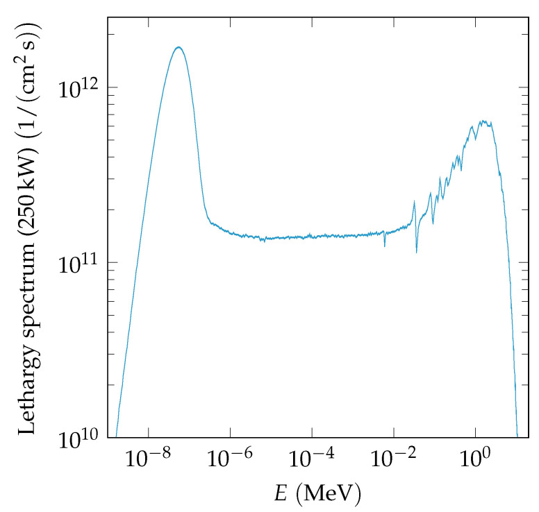
Samples 3 and 4 were irradiated in channel F19 of Core 189 at the TRIGA nuclear reactor of the Jožef Stefan Institute (JSI) [11] with neutrons. At this facility, the neutron energy spectrum goes from 10−8 MeV to 7 MeV [11,12]. The neutron lethargy spectrum () of the F19 channel in Core 189, which was used for all irradiations, is shown in Figure 1. Fast neutrons are defined as having an energy greater than 0.1 MeV. The fast neutron spectrum peaks between 1 MeV and 2 MeV. Fast neutron fluxes up to 4 × 10¹² n/(cm2 s) are available and were measured as a function of reactor power using gold foil activation [13]. To measure the fast neutron accumulated dose, the power of the reactor is set and the exposure time is recorded. This system typically measures the accumulated dose for each irradiation step to ∼10%.
Figure 1.
Lethargy neutron spectrum of channel F19 in Core 189 of the JSI TRIGA reactor used for all our neutron irradiations, at full reactor power (250 kW) [12].
4.3. Pion Irradiations
Samples 5, 6 and 7 were irradiated at PSI [14] with 200 MeV positive pions. Irradiations were performed by personnel from the CERN IRRAD facility [15]. The fluences were determined at CERN by measuring the activation in an aluminum foil mounted directly to each sample [16]. In addition to the statistical error, the CERN IRRAD website quotes an uncertainty of 20% for these measurements, due to the uncertainty on the hardness factor, which was added in quadrature to the statistical error.
5. Test Beam Analysis
The analysis of data in this work used the same analysis procedure and methods described in [4]. A brief description is given below and a detailed description can be found in [6,17].
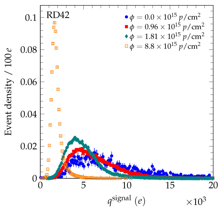
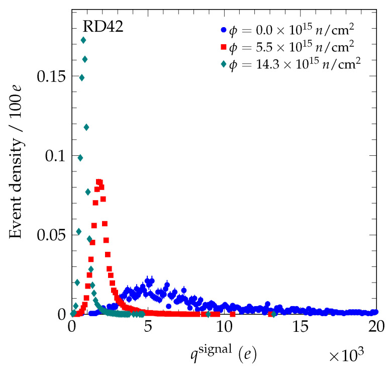
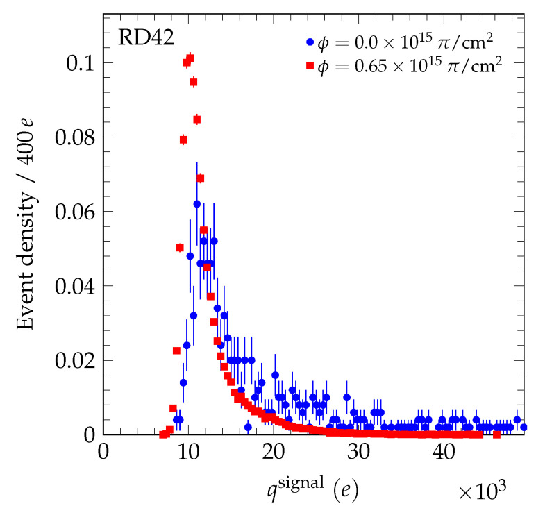
Data from an eight-plane silicon strip telescope [18], based on 50 pitch strip detectors with one or two floating intermediate strips, were used to reconstruct the predicted particle position in the diamond detector to roughly . A transparent reconstruction algorithm was used to reconstruct the signal charge (and actual position) of the particle in the diamond [4]. In this algorithm, the charge on the highest five contiguous strips within a 500 window of the predicted particle position are summed to calculate the signal charge and actual position of the particle in the diamond detector. In Figure 2, we present the evolution of the measured signal charge spectrum after the 70 MeV proton irradiations. In Figure 3, the evolution of the measured signal charge spectrum after neutron irradiations is shown. In all cases, the signal charge spectra get narrower with fluence and the average value decreases with fluence. In Figure 4, the measured signal charge spectrum of an scCVD diamond sensor before and after pion irradiation is shown. The average value of the spectrum decreases with fluence. The same overall effects were observed previously in the 24 GeV and 800 MeV proton irradiations [4,19].
Figure 2.
The signal charge spectrum evolution for samples irradiated with 70 MeV protons biased at . The pulse height spectrum before irradiation was measured using a setup with a 90Sr -source and a single pad metallization on the diamond. The integral of each spectrum has been normalized to unity.
Figure 3.
The signal charge spectrum evolution for samples irradiated with fast neutrons biased at . The pulse height spectrum before irradiation was measured using a setup with a 90Sr -source and a single pad metallization on the diamond. The integral of each spectrum was normalized to unity.
Figure 4.
The signal charge spectrum evolution for the scCVD diamond sample irradiated with 200 MeV pions biased at . The pulse height spectrum before irradiation was measured using a setup with a 90Sr -source and a single pad metallization on the diamond, biased at 1 V/, since the detector collects all the charge at a bias voltage of 200 V. The integral of each spectrum was normalized to unity.
The average distance an electron–hole pair drifts apart under the influence of an applied electric field or “charge collection distance” () was calculated from the measured signal charge spectrum by
| (1) |
where is the average of the measured signal charge spectrum in units of e and 36 e is the average number of electron–hole pairs created per micron for a minimum ionizing particle (MIP). We measured this quantity by evaluating the signal response of an unirradiated scCVD diamond sample to a 90Sr -source. After correcting the electronic gain, offset, and deposited charge, we determined the constant necessary to collect full charge. This measurement was performed for positive and negative bias polarity independently. The unirradiated scCVD diamond used was 497 thick. In a measurement cycle, we took data at multiple voltages up to V. In the source setup used, the electrons from 90Sr are 8% above minimum ionizing [9]. Our result, after all corrections, is () e/ for positive bias voltage and () e/ for negative bias voltage. These results are consistent with previous work [9,20,21]. The can be expressed by [22]
| (2) |
where t is the thickness of the diamond and is the average distance an electron or hole drifts in an infinitely thick sample of a given material. Using Equation (2), the schubweg or average total distance the electron–hole pair moves apart, defined as the sum , was calculated for each beam test measurement from the measured , assuming the ratio [4]. The effect of not knowing this ratio exactly was quantified in [4] and determined to not change the results of this analysis within the quoted errors.
6. Measurement of Damage Constants
After each irradiation step, the diamond devices were characterized in a 120 GeV hadron test beam at CERN. In a measurement cycle, the device under test was measured with both positive and negative bias voltage to obtain the sum of mean drift paths, , for an electric bias field of .
A first-order damage model was used to describe the irradiation damage effects. The model relates the inverse sum of mean drift paths, , linearly with the irradiation fluence by [23]:
| (3) |
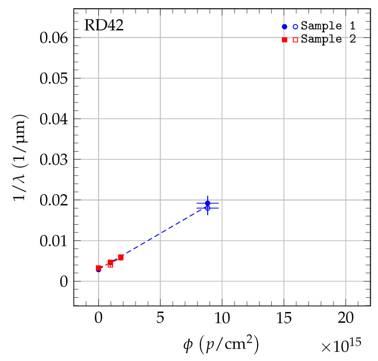
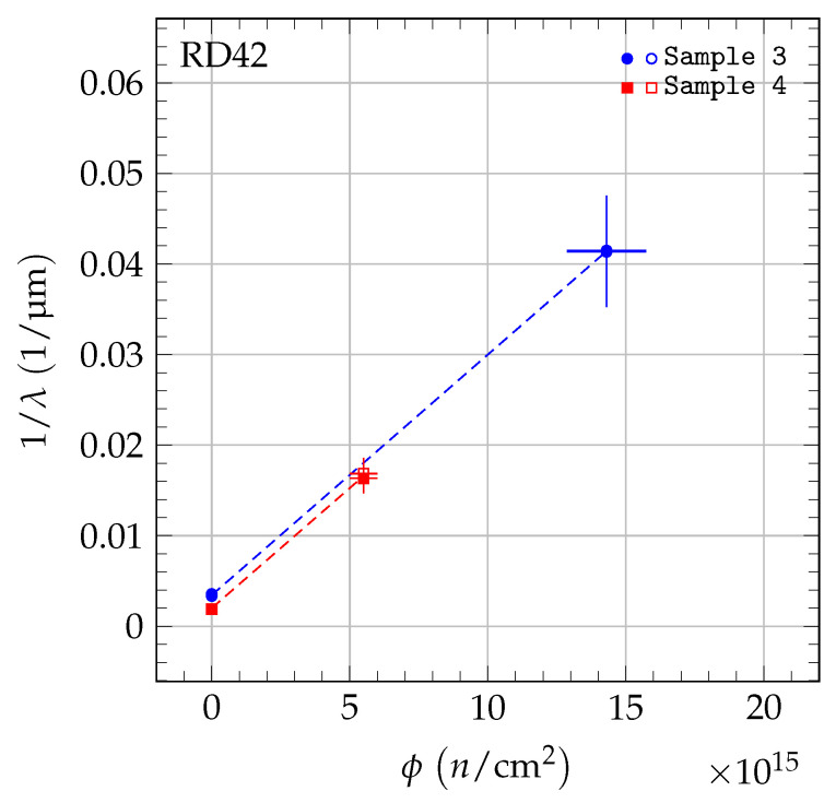
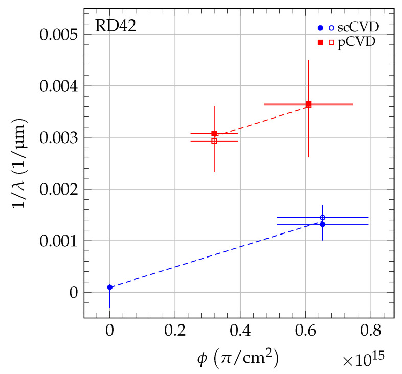
where k is the damage constant and accounts for charge traps in the unirradiated state. The inverse sum of mean drift paths as a function of irradiation fluence is shown in Figure 5 for 70 MeV proton irradiations, in Figure 6 for fast neutron irradiations, and in Figure 7 for 200 MeV pion irradiations. For each sample, the damage model was fitted to the data points to derive the slope. The damage constant of particle species i was derived from the slopes of the individual samples. For the pion irradiated samples, the damage model was fitted separately to the data of scCVD and pCVD diamond samples irradiated with pions and the observed damage constants were combined. The final results of the damage constants for 70 MeV proton irradiations, fast neutron irradiations and 200 MeV pion irradiations are:
Figure 5.
The for pCVD diamond in the 70 MeV proton irradiation. The two values shown at each fluence are the values for positive (solid markers) and negative (open markers) bias at . The data were fit with a first-order damage curve independently for each sample.
Figure 6.
The for pCVD diamond in the fast neutron irradiation. The two values shown at each fluence are the values for positive (solid markers) and negative (open markers) bias at . The data were fit with a first-order damage curve independently for each sample.
Figure 7.
The for scCVD and pCVD diamond in the pion irradiation. The two values shown at each fluence are the values for positive (solid markers) and negative (open markers) bias at . The data were fit with a simple damage curve independently for each diamond type. The uncertainty for unirradiated scCVD diamond comes from not knowing the upper initial mean drift distance exactly.
The general form of the statistical and systematic errors are given in [4]. Specifically, in this work, the statistical errors are dominated by the error in the fits while the systematic errors are dominated by the signal calibration, the pulse height dependence on track position and the pulse height dependence on bias polarity.
In Table 4, the relative damage constants are compared to the 24 GeV proton and 800 MeV proton results from [4] and to the 25 MeV proton results from [24]. The 70 MeV protons were found to be more than twice as damaging as 24 GeV protons; fast reactor neutrons were observed to be more than four times more damaging than 24 GeV protons; and 200 MeV pions were found to be more than three times as damaging as 24 GeV protons. These results are roughly consistent with displacement per atom (DPA) [25].
Table 4.
Relative damage constants for 24 GeV protons, 800 MeV protons, 70 MeV protons, 25 MeV protons, fast reactor neutrons, and 200 MeV pions. The radiation damage constants of 24 GeV protons and 800 MeV protons are from [4]. The relative radiation damage constant of 25 MeV protons is derived from [24].
| Particle Species | |
|---|---|
| 24 GeV protons | 1.0 |
| 800 MeV protons | 1.67 ± 0.09 |
| 70 MeV protons | 2.60 ± 0.29 |
| 25 MeV protons | 4.4 ± 1.2 |
| Fast neutrons | 4.3 ± 0.4 |
| 200 MeV pions | 3.2 ± 0.8 |
7. Universal Damage Curve
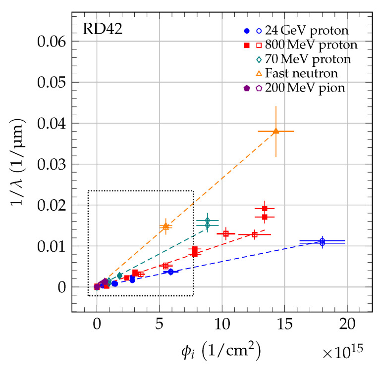
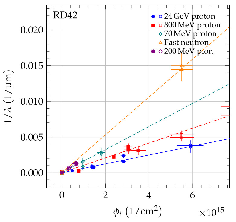
As shown in [4], scCVD and pCVD diamond follow the same damage model. However, the damage curve of species i for each diamond sample j starts at a different value of , due to the initial collection distance of the sample. The initial of sample j was derived by fitting a slope equal to the damage constant to the data points. Table 5 lists the parameter of the tested samples. In Figure 8, the as a function of fluence for 70 MeV proton, fast neutron, and 200 MeV pion irradiations is compared to the result of 24 GeV proton and 800 MeV proton irradiations [4] with the data points shifted by . The difference in slope of the dashed lines in this figure reflects the difference in damage constants. Figure 9 shows the data from Figure 8 in the dotted box to illustrate the relation of the low fluence data and the damage curves.
Table 5.
Parameter and fluence offset of diamond sample j for 70 MeV protons, fast reactor neutrons, and 200 MeV pions. The derived is not universal since it is sample dependent.
| Diamond j | (m) | (10/cm) |
|---|---|---|
| Sample 1 | 340 ± 21 | 4.7 ± 0.6 |
| Sample 2 | 318 ± 15 | 5.1 ± 0.6 |
| Sample 3 | 291 ± 21 | 5.5 ± 0.7 |
| Sample 4 | 531 ± 27 | 3.0 ± 0.4 |
| Sample 5 | 11,000 ± 20,000 | 0.15 ± 0.31 |
| Sample 6 + 7 | 420 ± 60 | 3.8 ± 0.7 |
Figure 8.
The for scCVD (solid markers) and pCVD (open markers) diamond. As reference, the 800 MeV proton and 24 GeV proton data from [4] are plotted. Each point is shifted by . The dotted box indicates the zoom area shown in Figure 9.
Figure 9.
The for scCVD (solid markers) and pCVD (open markers) diamond up to a fluence of 7 × 10¹⁵/cm2 (zoom of dotted box in Figure 8). As reference, the 800 MeV proton and 24 GeV proton data from [4] are plotted. Each point is shifted by .
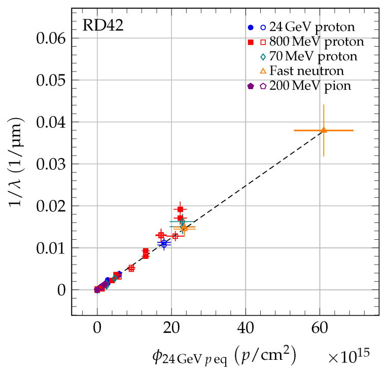
Since scCVD and pCVD diamond follow the same damage model in Equation (3) and different irradiations have different shift, it should be possible to generate a universal damage curve. To accomplish this, the fluences were scaled by
| (4) |
where is the relative radiation damage constant defined as . The measured as a function of 24 GeV proton equivalent fluence is shown in Figure 10 and illustrates the universality of the first-order radiation damage model described above.
Figure 10.
The for scCVD (solid markers) and pCVD (open markers) diamond. Each point is shifted by . The fluence of each point was scaled by the relative damage constant, , to the 24 GeV proton equivalent fluence. The damage model (dashed line) is fitted to the data points.
Instead of the offset , the separation of the damage curve of species i for individual diamond samples may be interpreted as a fluence offset, . Thus, the initial signal response of pCVD diamond corresponds to irradiated scCVD diamond. The fluence offset in units of 24 GeV proton equivalent fluence of each diamond sample was calculated using:
| (5) |
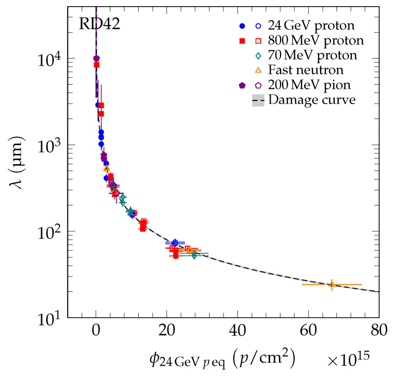
where is the damage constant for particle species i and the initial sum of mean drift paths of sample j derived from the fit to the data points of sample j with fixed . The fluence offset is listed in Table 5. To facilitate predictions of the signal response as a function of particle fluence, the measured of the five datasets were plotted as a function of 24 GeV proton equivalent fluence. To obtain a universal curve, the fluence of species i was scaled as in Equation (4) and each diamond data point was shifted by the fluence offset . The measured as a function of 24 GeV proton equivalent fluence of the data is presented in Figure 11.
Figure 11.
The for scCVD (solid markers) and pCVD (open markers) diamond. The fluence of each point was scaled by the relative damage constant to the 24 GeV proton equivalent fluence. Each point is shifted by which represents the starting value of sample j in 24 GeV proton equivalent fluence space. The dashed line is the fit of the damage model in Equation (3) to the data points. The gray band indicates the variation of the fit parameters by one standard deviation.
8. Measurement of the / Ratio
The initial non-uniformities in unirradiated pCVD material are mainly due to the interior crystal structure where single grains have different charge collection properties causing a spatial variation of the Landau-like distributions in the material [19]. This effect was clearly demonstrated in [4] where we showed the quantity R,
| (6) |
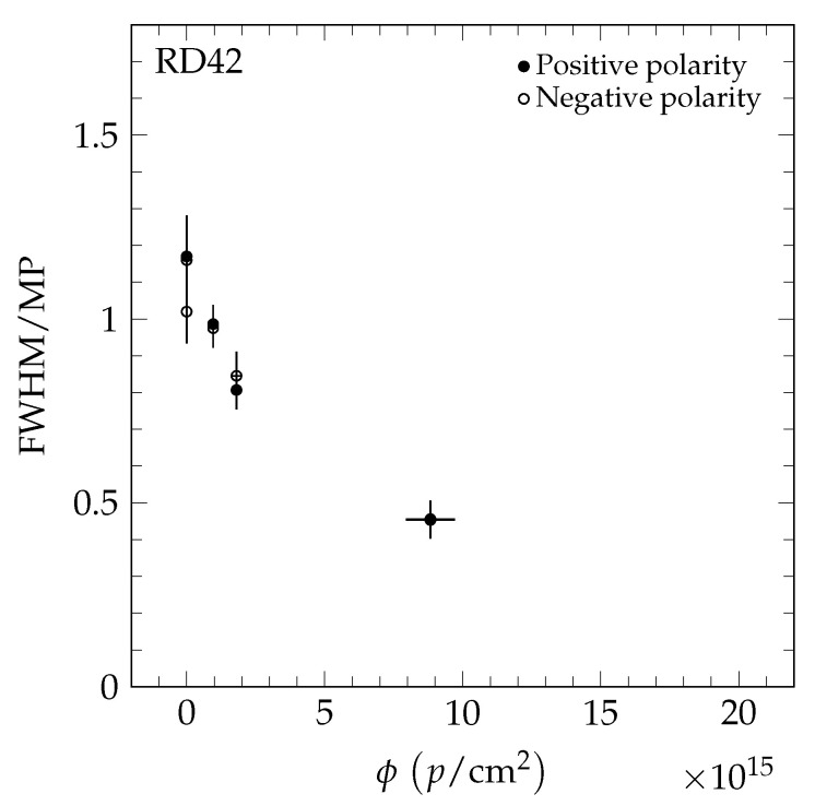
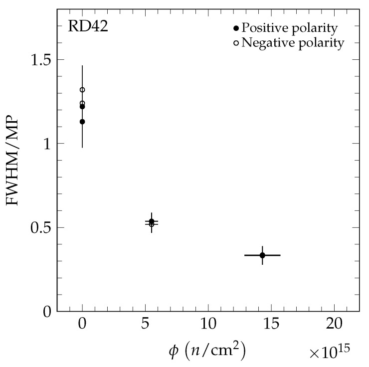
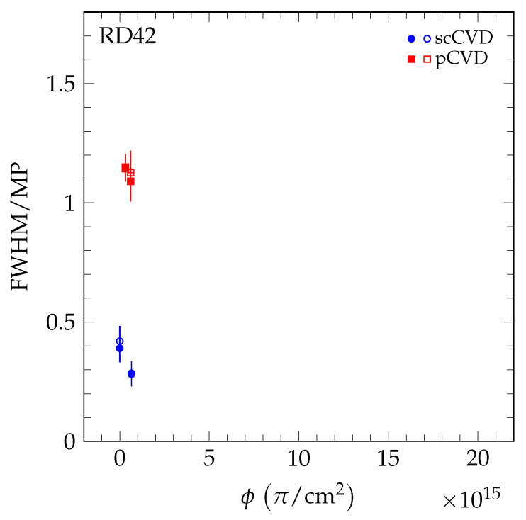
is also a measure of the uniformity of the material. The smaller the quantity R the narrower the normalized signal charge distribution is across the material. Here, we used the full width at half maximum () normalized by the most probable value () of the signal response [4] to analyze its irradiation dependence (we normalized to , since the inherent distribution is Landau-like and for Landau distributions the measured mean depends on the number of events attained). To compare with previous beam test results for R, we used a hadron beam, which is near minimum ionizing, as we did previously [4].
The results of the 70 MeV proton irradiations are shown in Figure 12. The results of the neutron irradiations are presented in Figure 13. The value R decreases for both irradiation species as a function of fluence, confirming the observation with pCVD diamond in [4]. The value R as a function of 200 MeV pion fluence is shown in Figure 14 and is compatible with the findings in [4].
Figure 12.
The as a function of fluence in the 70 MeV proton irradiation measured in a hadron beam at CERN. The two values shown at each fluence are the values for positive (solid markers) and negative bias (open markers) at .
Figure 13.
The as a function of fluence in the fast neutron irradiation measured in a hadron beam at CERN. The two values shown at each fluence are the values for positive (solid markers) and negative bias (open markers) at .
Figure 14.
The as a function of fluence in the pion irradiation measured in a hadron beam at CERN. The two values shown at each fluence are the values for positive (solid markers) and negative bias (open markers) at .
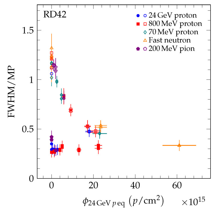
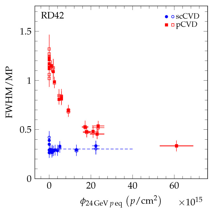
To compare the results of the different particle species, the fluence of each data point was scaled to 24 GeV proton equivalent fluence using Equation 4. In Figure 15, the value R of the five datasets (24 GeV protons [4], 800 MeV protons [4], 70 MeV protons, fast neutrons, and 200 MeV pions) is shown as a function of 24 GeV proton equivalent fluence. The pCVD data all fall on a single curve which decreases with fluence. The scCVD data all fall on a different curve, which is compatible with being flat with fluence. This is illustrated in Figure 16 where scCVD diamond data are shown in blue and pCVD diamond data are shown in red. The two curves taken together indicate the pCVD samples are becoming more uniform with irradiation and approaching the uniformity of single-crystal diamond.
Figure 15.
The for scCVD (solid markers) and pCVD (open markers) diamond. The fluence of each point was scaled by the relative damage constant to the 24 GeV proton equivalent fluence.
Figure 16.
The of scCVD and pCVD diamond samples irradiated with 24 GeV protons, 800 MeV protons, 70 MeV protons, fast reactor neutron, and 200 MeV pions for positive (solid markers) and negative bias (open markers) at . The fluence of each point was scaled by the relative damage constant to the 24 GeV proton equivalent fluence. The dashed line represents a constant fit to the scCVD diamond data points (blue) extrapolated to 40 × 1015 p/cm2 for illustrative purposes.
9. Comparison with Silicon
Once the damage constants are determined, the damage constants for diamond may be compared with the damage constants for silicon. The collected charge in silicon devices depends on the electric field and trapping times. The trapping time at a temperature T and time after irradiation, t, is inversely proportional to the fluence [26,27]:
| (7) |
From the measurements of trapping times which require a fully depleted detector, the mean drift path of the charge carriers, , may be calculated using the relation
| (8) |
where are the drift velocities of electrons and holes, respectively. Using Equations (7) and (8), as a function of fluence for silicon may be described by
| (9) |
where k is a damage constant.
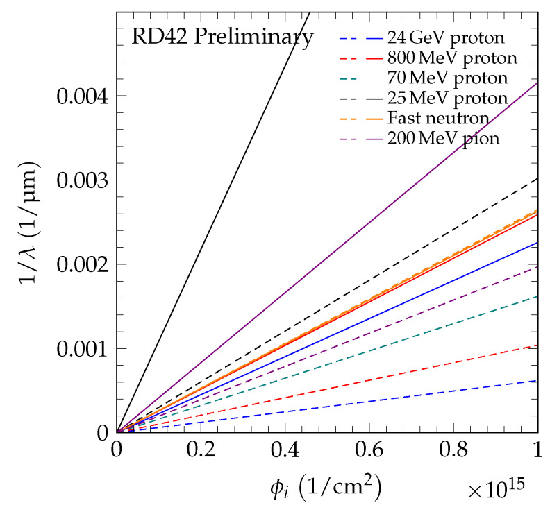
As shown in Figure 17, the damage constants measured at an electric field of 2 V/ and at for diamond and silicon were used to generate the inverse sum of mean drift paths versus fluence plot up to a fluence of 1015 particles/cm2. The dashed lines are the diamond results from this work and those in [4,24] for the irradiations of 24 GeV protons (blue), 800 MeV protons (red), 70 MeV protons (green), 25 MeV protons (black), fast neutrons (orange), and 200 MeV pions (purple). The solid lines are the silicon data from RD50 [28] for proton (blue and red), pion (purple) and neutron (orange) irradiations and data from [24] for 25 MeV proton (black) irradiations. The sum of mean drift paths is obtained from charge collection measurements at room temperature, assuming a uniform electric field of 2 V/. Drift velocities at 2 V/ were derived from [29] and trapping times were taken from [27] after 80 of annealing at 60 .
Figure 17.
The for CVD diamond and silicon for proton, neutron and pion irradiations at an electric field of 2 V/. The charge collection was measured at room temperature. The dashed lines are diamond results from this work and those in [4] for irradiations at 24 GeV protons (blue), 800 MeV protons (red), 70 MeV protons (green), fast neutrons (orange), and 200 MeV pions (purple), and the solid lines are the silicon damage data from RD50 [28] for proton (blue and red), neutron (orange), and pion (purple) irradiations. The curves for irradiations with 25 MeV protons were taken from [24].
The results in Figure 17 show that for proton and pion irradiations diamond is much less radiation sensitive than silicon (greater than a factor of two) for all proton and pion energies measured, while for neutron irradiations silicon is comparable in radiation tolerance to diamond.
10. Summary
A study of CVD diamond material before and after a series of irradiations with 70 MeV protons, fast reactor neutrons and 200 MeV pions is presented. The decrease in signal response is in agreement with a first order damage model. The measured data were compared to previous measurements of CVD diamond samples irradiated with 800 MeV protons and 24 GeV protons [4]. Furthermore, the five datasets were combined in a universal damage curve for diamond material which allows predictions to be made for potential applications.
The decrease in of the signal response of the collected charge as a function of particle fluence was confirmed for pCVD diamond material irradiated with 70 MeV protons and fast reactor neutrons. Moreover, the measurements presented in this paper were combined with previous measurements [4] into a universal curve.
Finally, the radiation damage constants of diamond were compared to the radiation damage constants of silicon. For proton irradiations, diamond was found to be more radiation tolerant than silicon, while a comparable radiation tolerance against neutrons was observed.
Acknowledgments
The RD42 Collaboration gratefully acknowledges the staff at CERN for test beam time, their help in setting up the beam conditions, and for their assistance in making our tests a success. We also thank Profs. T. Shinozuka, T. Wakui, and the staff of the CYRIC Irradiation Facility at Tohoku University in Sendai, Japan for their help in the 70 MeV proton irradiations (Experiments 8705 and 9214) and the staff of the TRIGA Nuclear Reactor at the Jožef Stefan Institute in Ljubljana, Slovenia for their help in making the neutron irradiations possible.
Author Contributions
Software, F.B., L.B., G.C. (Gilles Claus), M.G. (Mathieu Goffe), M.R., D.A.S.B., and R.W.; Formal Analysis, F.B., L.B., D.H., H.K., G.K., M.M. (Marko Mikuž), A.O., and W.T.; Investigation, V.B., E.D., M.P., B.S. (Bruno Sopko), V.S., A.A., M.A., F.B., L.B., M.R.B., H.C.B., V.B. (Vincenzo Bellini), B.B., A.B., J.-M.B., G.C. (Gabriele Chiodini), D.C., V.C., G.C. (Gilles Claus), J.C. (Johann Collot), J.C. (John Cumalat), S.C., A.E.D., R.D., D.D., W.d.B., C.D., M.D., G.E., V.E., J.F., L.G.-M., M.-L.G.-M., K.K.G., M.G. (Martin Gastal), A.G. (Abderrahman Ghimouz), M.G. (Mathieu Goffe), J.G., A.G. (Alexander Golubev), A.G. (Andrej Gorišek), E.G., J.G.-K., A.G. (Aidan Grummer), B.H., D.H., M.H., J.H., F.H., C.H., J.J., H.K., K.K., R.K., M.K., G.K., S.K., A.L., S.L., A.L.G., I.L.P., E.L., C.M. (Chaker Maazouzi), I.M., S.M. (Sara Marcatili), A.M. (Alysia Marino), C.M. (Cédric Mathieu), M.M. (Mauro Menichelli), M.M. (Marko Mikuž), A.M. (Arianna Morozzi), F.M., J.M., R.M., A.O., P.O., D.P., H.P., R.P. (Roberto Perrino), F.P., R.P. (Renato Potenza), A.Q., F.R., A.R., M.R., S.R., O.R., D.A.S.B., C.J.S., S.S. (Stephen Schnetzer), S.S. (Silvio Sciortino), A.S., S.S. (Sally Seidel), L.S., D.S.S., S.S. (Stefania Spagnolo), S.S. (Stefan Spanier), K.S., R.S., B.S. (Bjarne Stugu), C.S., M.T. (Michael Traeger), W.T., M.T. (Marco Truccato), C.T., J.V., S.W., R.W., J.W. (Jianchun Wang), N.W., J.W. (Jayashani Wickramasinghe), M.Y., J.Z., M.Z., K.H., Y.I., O.J., T.K., S.M. (Shingo Mitsui), R.N., S.T., and Y.U.; Data Curation, F.B., L.B., M.G. (Mathieu Goffe), A.G. (Andrej Gorišek), D.H., J.J., H.K., G.K., A.O., M.R., D.A.S.B., S.S. (Sally Seidel), R.W., K.H., Y.I., O.J., T.K., S.M. (Shingo Mitsui), R.N., S.T., and Y.U.; Writing, F.B., L.B., D.H., H.K., G.K., A.O., and W.T.; Supervision, M.A., W.d.B., J.-M.B., G.C. (Gabriele Chiodini), G.E., V.E., M.-L.G.-M., J.G., A.G. (Alexander Golubev), F.H., H.K., M.K., M.M. (Marko Mikuž), J.M., A.O., P.O., H.P., R.P. (Renato Potenza), A.Q., S.S. (Stephen Schnetzer), S.S. (Silvio Sciortino), S.S. (Sally Seidel), L.S., S.S. (Stefan Spanier), W.T., C.T., S.W., R.W., and N.W.; Project Administration, H.K. and W.T.; and Funding Acquisition, J.-M.B., J.G., H.K., M.M. (Marko Mikuž), J.M., A.O., H.P., A.Q., S.S. (Sally Seidel), S.S. (Stephen Schnetzer), W.T., R.W., N.W., K.H., S.T., and Y.U. All authors have read and agreed to the published version of the manuscript.
Funding
The research leading to these results received funding from the European Union’s Horizon 2020 research and innovation program under grant agreement No. 654168. This work was also partially supported by the Swiss National Science Foundation grant #20FL20_154216, ETH grant 51 15-1, Swiss Government Excellence Scholarship ESKAS No. 2015.0808, UK Science and Technology Facilities Council grant ST/M003965/1 and the U.S. Department of Energy through grant DE-SC0011726.
Conflicts of Interest
The authors declare no conflict of interest.
Footnotes
Publisher’s Note: MDPI stays neutral with regard to jurisdictional claims in published maps and institutional affiliations.
References
- 1.CERN The European Organization for Nuclear Research, CH-1211, Genève 23, Switzerland. [(accessed on 11 November 2020)]; Available online: https://home.cern/
- 2.Apollinari G., Brüning O., Nakamoto T., Lucio R. High-Luminosity Large Hadron Collider (HL-LHC): Preliminary Design Report, Chapter 1: High-Luminosity Large Hadron Collider HL-LHC. CERN; Geneva, Switzerland: 2015. CERN Yellow Reports: Monographs, CERN-2015-005. [DOI] [Google Scholar]
- 3.Apollinari G., Béjar A.I., Brüning O., Fessia P., Lamont M., Rossi L., Tavian L. High-Luminosity Large Hadron Collider (HL-LHC): Technical Design Report V.0.1. CERN; Geneva, Switzerland: 2017. CERN Yellow Reports: Monographs, Volume 4/2017 CERN-2017-007-M. [DOI] [Google Scholar]
- 4.Bäni L., Alexopoulos A., Artuso M., Bachmair F., Bartosik M., Beck H., Bellini V., Belyaev V., Bentele B., Bes A., et al. ((On behalf of the RD42 Collaboration)). A study of the radiation tolerance of poly-crystalline and single-crystalline CVD diamond to 800 MeV and 24 GeV protons. J. Phys. D Appl. Phys. 2019;52:465103. doi: 10.1088/1361-6463/ab37c6. [DOI] [Google Scholar]
- 5.The Samples Used in this Study Were Electronic Grade CVD Diamond Purchased from Element Six Technologies, Global Innovation Centre, Fermi Ave., Harwell, OX11 0QR, United Kingdom and II-VI Incorporated, 375 Saxonburg Blvd., Saxonburg, PA 16056-9499, USA. [(accessed on 11 November 2020)]; Available online: http://www.iiviinfrared.com.
- 6.Bachmair F. Ph.D. Thesis. ETH Zürich; Zürich, Switzerland: 2016. CVD Diamond Sensors in Detectors for High Energy Physics. [DOI] [Google Scholar]
- 7.Dotite Silver Paint D-550 Fujikura Kasei Co., LTD. 6-15, Shibakoen 2-chome, Minato-ku, Tokyo 105-0011 Japan. [(accessed on 30 September 2020)]; Available online: https://www.fkkasei.co.jp/english/product/electric/dotite/05.html.
- 8.Integrated Detector and Electronics (IDE) AS Designed the VA Circuits. [(accessed on 11 November 2020)]; Available online: http://www.ideas.no.
- 9.Zhao S. Ph.D. Thesis. The Ohio State University; Columbus, OH, USA: 1994. [(accessed on 30 September 2020)]. Characterization of the Electrical Properties of Polycrystalline Diamond Films. Available online: http://rave.ohiolink.edu/etdc/view?acc_num=osu1394810346. [Google Scholar]
- 10.Cyclotron and Radioisotope Center (CYRIC), Tohoku University, Sendai, Miyagi, Japan. [(accessed on 11 November 2020)]; Available online: http://www.cyric.tohoku.ac.jp.
- 11.Snoj L., Žerovnik G., Trkov A. Computational analysis of irradiation facilities at the JSI TRIGA reactor. Appl. Radiat. Isot. 2012;70:483. doi: 10.1016/j.apradiso.2011.11.042. [DOI] [PubMed] [Google Scholar]
- 12.Ambrožič K., Žerovnik G., Snoj L. Computational analysis of the dose rates at JSI TRIGA reactor irradiation facilities. Appl. Radiat. Isot. 2017;130:140. doi: 10.1016/j.apradiso.2017.09.022. [DOI] [PubMed] [Google Scholar]
- 13.Krištof E.S. Characterization of neutron flux in the exposure channel F19 of the TRIGA Mark II reactor in Ljubljana. Nucl. Energy Cent. Eur. 1998;98:43. [Google Scholar]
- 14.Paul Scherrer Institute (PSI), 5232 Villigen, Switzerland. [(accessed on 11 November 2020)]; Available online: https://www.psi.ch.
- 15.CERN IRRAD Proton Facility. [(accessed on 30 September 2020)]; Available online: https://ps-irrad.web.cern.ch/ps-irrad/external.php.
- 16.Glaser M., Ravotti F., Moll M. Dosimetry assessments in the irradiation facilities at the CERN-PS accelerator. IEEE Trans. Nucl. Sci. 2006;53:2016–2022. doi: 10.1109/TNS.2006.880569. [DOI] [Google Scholar]
- 17.Bäni L. Ph.D. Thesis. ETH Zürich; Zürich, Switzerland: 2017. Top Quarks and Diamonds. [DOI] [Google Scholar]
- 18.Colledani C., Dulinski W., Turchetta R., Djama F., Rudge A., Weilhammer P. A Submicron Precision Silicon Telescope for Beam Test Purposes. Nucl. Instruments Methods Phys. Res. Sect. A Accel. Spectrometers Detect. Assoc. Equip. 1996;372:379–384. doi: 10.1016/0168-9002(95)01414-4. [DOI] [Google Scholar]
- 19.Meier D. Ph.D. Thesis. Universität Heidelberg; Heidelberg, Germany: 1999. CVD Diamond Sensors for Particle Detection and Tracking. [Google Scholar]
- 20.Pan L.S., Han S., Kania D.R., Zhao S., Gan K.K., Kagan H., Kass R., Malchow R., Morrow F., Palmer W.F., et al. Particle- and photoinduced conductivity in type-IIa diamonds. J. Appl. Phys. 1993;74:1086. doi: 10.1063/1.354957. [DOI] [Google Scholar]
- 21.Muškinja M., Cindro V., Gorišek A., Kagan H., Kramberger G., Mandić I., Mikuž M., Phan S., Smith D.S., Zavrtanik M. Investigation of charge multiplication in single crystalline CVD diamond. Nucl. Instruments Methods Phys. Res. Sect. A. 2017;841:162–169. doi: 10.1016/j.nima.2016.10.018. [DOI] [Google Scholar]
- 22.Hecht K. Zum Mechanismus des lichtelektrischen Primärstromes in isolierenden Kristallen. Z. Phys. 1932;77:235. doi: 10.1007/BF01338917. [DOI] [Google Scholar]
- 23.The RD42 Collaboration. Hartjes F., Adam W., Bauer C., Berdermann E., Bergonzo P., Bogani F., Borchi E., Brambilla A., Bruzzi M., et al. Parameterisation of Radiation Effects on CVD Diamond for Proton Irradiation. Nucl. Phys. B Proc. Suppl. 1999;78:675. doi: 10.1016/S0920-5632(99)00623-4. [DOI] [Google Scholar]
- 24.Tsung J.W., Havranek M., Hügging F., Kagan H., Krüger H., Wermes N. Signal and noise of diamond pixel detectors at high radiation fluences. J. Instrum. 2012;7:P09009. doi: 10.1088/1748-0221/7/09/P09009. [DOI] [Google Scholar]
- 25.Guthoff M., de Boer W., Müller S. Simulation of beam induced lattice defects of diamond detectors using FLUKA. Nucl. Instruments Methods Phys. Res. Sect. A Accel. Spectrometers Detect. Assoc. Equip. 2014;735:223–228. doi: 10.1016/j.nima.2013.08.083. [DOI] [Google Scholar]
- 26.Kramberger G., Cindro V., Mandić I., Mikuž M., Zavrtanik M. Determination of effective trapping times for electrons and holes in irradiated silicon. Nucl. Instruments Methods Phys. Res. Sect. A Accel. Spectrometers Detect. Assoc. Equip. 2002;476:645–651. doi: 10.1016/S0168-9002(01)01653-9. [DOI] [Google Scholar]
- 27.Cindro V., Kramberger G., Lozano M., Mandić I., Mikuž M., Pellegrini G., Pulko J., Ullan M., Zavrtanik M. Radiation damage in p-type silicon irradiated with neutrons and protons. Nucl. Instruments Methods Phys. Res. Sect. A Accel. Spectrometers Detect. Assoc. Equip. 2009;599:60–65. doi: 10.1016/j.nima.2008.11.007. [DOI] [Google Scholar]
- 28.RD50 Collaboration. [(accessed on 11 November 2020)]; Available online: http://rd50.web.cern.ch/rd50/
- 29.Jacoboni C., Canali C., Ottaviani G., Alberigi Quaranta A. A review of some charge transport properties of silicon. Solid-State Electron. 1977;20:77. doi: 10.1016/0038-1101(77)90054-5. [DOI] [Google Scholar]


