NIHPA Author Manuscripts logoLink to NIHPA Author Manuscripts
. Author manuscript; available in PMC: 2021 Oct 22.
Published in final edited form as: Phys Med Biol. 2020 Oct 22;65(21):21RM01. doi: 10.1088/1361-6560/ab9500

Roadmap toward the 10 ps time-of-flight PET challenge

Paul Lecoq 1, Christian Morel 2, John O Prior 3, Dimitris Visvikis 4, Stefan Gundacker 1,5, Etiennette Auffray 1, Peter Križan 6, Rosana Martinez Turtos 1,21, Dominique Thers 7, Edoardo Charbon 8, Joao Varela 9, Christophe de La Taille 10, Angelo Rivetti 11, Dominique Breton 12, Jean-François Pratte 13, Johan Nuyts 14, Suleman Surti 15, Stefaan Vandenberghe 16, Paul Marsden 17, Katia Parodi 18, Jose Maria Benlloch 19, Mathieu Benoit 20
PMCID: PMC7721485  NIHMSID: NIHMS1642255  PMID: 32434156

Abstract

Since the seventies, positron emission tomography (PET) has become an invaluable medical molecular imaging modality with an unprecedented sensitivity at the picomolar level, especially for cancer diagnosis and the monitoring of its response to therapy. More recently, its combination with x-ray computed tomography (CT) or magnetic resonance (MR) has added high precision anatomic information in fused PET/CT and PET/MR images, thus compensating for the modest intrinsic spatial resolution of PET. Nevertheless, a number of medical challenges call for further improvements in PET sensitivity. These concern in particular new treatment opportunities in the context personalized (also called precision) medicine, such as the need to dynamically track a small number of cells in cancer immunotherapy or stem cells for tissue repair procedures. A better signal-to-noise ratio (SNR) in the image would allow detecting smaller size tumours together with a better staging of the patients, thus increasing the chances of putting cancer in complete remission. Moreover, there is an increasing demand for reducing the radioactive doses injected to the patients without impairing image quality.

There are three ways to improve PET scanner sensitivity: improving detector efficiency, increasing geometrical acceptance of the imaging device and pushing the timing performance of the detectors. Currently, some pre-localization of the electron-positron annihilation along a line-of-response (LOR) given by the detection of a pair of annihilation photons is provided by the detection of the time difference between the two photons, also known as the time-of-flight (TOF) difference of the photons, whose accuracy is given by the coincidence time resolution (CTR). A CTR of about 10 picoseconds FWHM will ultimately allow to obtain a direct 3D volume representation of the activity distribution of a positron emitting radiopharmaceutical, at the millimetre level, thus introducing a quantum leap in PET imaging and quantification and fostering more frequent use of 11C radiopharmaceuticals.

The present roadmap article toward the advent of 10 ps TOF-PET addresses the status and current/future challenges along the development of TOF-PET with the objective to reach this mythic 10 ps frontier that will open the door to real-time volume imaging virtually without tomographic inversion. The medical impact and prospects to achieve this technological revolution from the detection and image reconstruction point-of-views, together with a few perspectives beyond the TOF-PET application are discussed.

Keywords: positron emission tomography, detection of annihilation photons, photo-detectors, image reconstruction, 10 ps TOF-PET

References

  1. Acerbi F et al. 2017. Cryogenic characterization of FBK HD near-UV sensitive SiPMs IEEE Trans. Electron Devices 64 521–6 [Google Scholar]
  2. Acerbi F and Gundacker S 2019. Understanding and simulating SiPMs Nucl. Instrum. Methods Phys. Res. A 926 16–35 [Google Scholar]
  3. Aglieri Rinella G et al. 2019. The NA62 GigaTracKer: a low mass high intensity beam 4D tracker with 65 ps time resolution on tracks (arXiv:1904.12837) [Google Scholar]
  4. Ahn S. et al. Joint estimation of activity and attenuation for PET using pragmatic MR-based prior: application to clinical TOF PET/MR whole-body data for FDG and non-FDG tracers. Phys. Med. Biol. 2018;63:045006. doi: 10.1088/1361-6560/aaa8a6. [DOI] [PubMed] [Google Scholar]
  5. Amaudruz P et al. 2009. Simultaneous reconstruction of scintillation light and ionization charge produced by 511 keV photons in liquid xenon: potential application to PET Nucl. Instrum. Methods Phys. Res. A 607 668–76 [Google Scholar]
  6. Aprile E, Curioni A, Giboni KL, Kobayashi M, Oberlack UG and Zhang S 2008. Compton imaging of MeV gamma-rays with the liquid xenon gamma-ray imaging telescope (LXeGRIT) Nucl. Instrum. Methods Phys. Res. A 593 414–25 [Google Scholar]
  7. Aprile E and Doke T 2010. Liquid xenon detectors for particle physics and astrophysics Rev. Mod. Phys 82 2053–97 [Google Scholar]
  8. Ariño-Estrada G, Mitchell GS, Kwon SI, Du J, Kim H, Cirignano LJ, Shah KS and Cherry SR 2018. Towards time-of-flight PET with a semiconductor detector Phys. Med. Biol 63 04LT01. [DOI] [PMC free article] [PubMed] [Google Scholar]
  9. ASCIMAT 2020. Increasing the scientific excellence and innovation capacity in Advanced Scintillation Materials of the Institute of Physics from the Czech Academy of Sciences, European TWIN project grant agreement 690599 (http://www.h2020-ascimat.com) (Accessed: 14 June 2020)
  10. Badawi RD et al. 2019. First human imaging studies with the EXPLORER total-body PET scanner J. Nucl. Med 60 299–303 [DOI] [PMC free article] [PubMed] [Google Scholar]
  11. Baumgarten HD and Flake AW 2019. Fetal surgery Pediatr. Clin. North Am 66 295–308 [DOI] [PubMed] [Google Scholar]
  12. Benoit M. Pixel detector R&D for the compact linear collider. J. Instrum. 2019;14:C06003. [Google Scholar]
  13. Berdalovic I. et al. Monolithic pixel development in TowerJazz 180 nm CMOS for the outer pixel layers in the ATLAS experiment. J. Instrum. 2018;13:C01023. [Google Scholar]
  14. Berg E and Cherry SR 2018. Using convolutional neural networks to estimate time-of-flight from PET detector waveforms Phys. Med. Biol 63 02LT01. [DOI] [PMC free article] [PubMed] [Google Scholar]
  15. Berker Y and Li Y 2016. Attenuation correction in emission tomography—a review Med. Phys 43 807–32 [DOI] [PMC free article] [PubMed] [Google Scholar]
  16. Biassoni L and Easty M 2017. Paediatric nuclear medicine imaging Br. Med. Bull 123 127–48 [DOI] [PubMed] [Google Scholar]
  17. Bornheim A et al. 2017. Precision timing calorimetry with the upgraded CMS crystal ECAL Proc. Int. Conf. on Technology and Instrumentation in Particle Physics 2017 ed Z A Liu vol 213 (Berlin: Springer) ( 10.1007/978-981-13-1316-5_8) [DOI] [Google Scholar]
  18. Braga LHC et al. 2013. An 8 × 16-pixel 92kSPAD time-resolved sensor with on-pixel 64ps 12b TDC and 100MS/s real-time energy histogramming in 0.13microm CIS technology for PET/MRI applications Proc. IEEE Int. Solid-State Circuits Conf (San Francisco, CA) pp 486–7 [Google Scholar]
  19. Breton D, Delagnes E and Maalmi J 2009. Picosecond time measurement using ultra-fast analog memories Proc. of TWEPP-09 (Paris, France) pp 149–54 [Google Scholar]
  20. Breton D, De Cacqueray V, Delagnes E, Grabas H, Maalmi J, Minafra N, Royon C and Saimpert M 2016. Measurements of timing resolution of ultra-fast silicon detectors with the SAMPIC waveform digitizer Nucl. Instrum. Methods A 835 51–60 [Google Scholar]
  21. Breton D, Delagnes E, Maalmi J and Rusquart P 2014. The WaveCatcher family of SCA-based 12-bit 3.2-GS/s fast digitizers Conf. Rec. IEEE Real-Time pp 1–8 [Google Scholar]
  22. Brunner S and Schaart D 2017. Enabling cost-effective TOF-PET by exploiting the Cherenkov emission in BGO J. Nucl. Med 58 150 [Google Scholar]
  23. Budinger TF 1983. Time-of-flight positron emission tomography—status relative to conventional PET J. Nucl. Med 24 73–76 [PubMed] [Google Scholar]
  24. Buitenhuis HJT, Diblen F, Brzezinski KW, Brandenburg S and Dendooven P 2017. Beam-on imaging of short-lived positron emitters during proton therapy Phys. Med. Biol 62 4654–72 [DOI] [PubMed] [Google Scholar]
  25. Burgess AE 2011. Visual perception studies and observer models in medical imaging Semin. Nucl. Med 41 419–36 [DOI] [PubMed] [Google Scholar]
  26. Cai Z, Li S, Matuskey D, Nabulsi N and Huang Y 2019. PET imaging of synaptic density: a new tool for investigation of neuropsychiatric diseases Neurosci. Lett 691 44–50 [DOI] [PMC free article] [PubMed] [Google Scholar]
  27. Campbell M. et al. Towards a new generation of pixel detector readout chips. J. Instrum. 2016;11:C01007. [Google Scholar]
  28. Carniti P. et al. CLARO-CMOS, a very low power ASIC for fast photon counting with pixellated photodetectors. J. Instrum. 2012;7:P11026. [Google Scholar]
  29. Carson RE and Kuo PH 2019. Brain-dedicated emission tomography systems: a perspective on requirements for clinical research and clinical needs in brain imaging IEEE Trans. Radiat. Plasma Med. Sci 3 254–61 [Google Scholar]
  30. Cartiglia N et al. 2017. Beam test results of a 16 ps timing system based on ultra-fast silicon detectors Nucl. Instrum. Methods A 850 83–88 [Google Scholar]
  31. Cates JW, Gundacker S, Auffray E, Lecoq P and Levin CS 2018. Improved single photon time resolution for analog SiPMs with front end readout that reduces influence of electronic noise Phys. Med. Biol 63 185022. [DOI] [PubMed] [Google Scholar]
  32. Chan KL et al. 2017. A 32.75-Gb/s voltage-mode transmitter with three-tap FFE in 16-nm CMOS IEEE J. Solid-State Circuits 52 2663–78 [Google Scholar]
  33. Chepel V, Lopes MI, Kuchenkov A, Ferreira Marques R and Policarpo AJPL 1997. Performance study of liquid xenon detector for PET Nucl. Instrum. Methods Phys. Res. A 392 427–32 [Google Scholar]
  34. Cherenkov PA 1934. Visible emission of clean liquids by action of radiation Doklady Akademii Nauk SSSR vol 2 p 451 [Google Scholar]
  35. Cherry SR. et al. Total-body imaging: transforming the role of positron emission tomography. Sci. Transl. Med. 2017;9:eaaf6169. doi: 10.1126/scitranslmed.aaf6169. [DOI] [PMC free article] [PubMed] [Google Scholar]
  36. Cherry SR, Jones T, Karp JS, Qi J, Moses WW and Badawi RD 2018. Total-body PET: maximizing sensitivity to create new opportunities for clinical research and patient care J. Nucl. Med 59 3–12 [DOI] [PMC free article] [PubMed] [Google Scholar]
  37. Cherry SR, Sorenson JA and Phelps ME 2012. Physics in Nuclear Medicine e-Book (Amsterdam: Elsevier; ) [Google Scholar]
  38. Collazuol G. The SiPM physics and technology–a review. Proc. of the Int. Workshop on New Photon-Detectors (PhotoDet 2012) (Orsay, France) 2012 [Google Scholar]
  39. Consuegra D, Dolenec R, Korpar S, Križan P, Pestotnik R and Razdevšek G 2020. Simulation study to improve the performance of a whole-body PbF2 Cherenkov TOF-PE0T scanner Phys. Med. Biol 65 055013. [DOI] [PubMed] [Google Scholar]
  40. Conti M and Bendriem B 2019. The new opportunities for high time resolution clinical TOF PET Clin. Transl. Imaging 7 139–47 [Google Scholar]
  41. Crespo P, Shakirin G, Fiedler F, Enghardt W and Wagner A 2007. Direct time-of-flight for quantitative, real-time in-beam PET: a concept and feasibility study Phys. Med. Biol 52 6795–811 [DOI] [PubMed] [Google Scholar]
  42. Crystal Clear Collaboration RD18, CERN/DRDC/P27/91–15 (https://cds.cern.ch/record/291227)
  43. de La Taille C. et al. ALTIROC0, a 20 pico-second time resolution ASIC for the ATLAS high granularity timing detector (HGTD) PoS (TWEPP-17) 2018;313:006. [Google Scholar]
  44. Defrise M, Rezaei A and Nuyts J 2012. Time-of-flight PET data determine the attenuation sinogram up to a constant Phys. Med. Biol 57 885–99 [DOI] [PubMed] [Google Scholar]
  45. Defrise M, Rezaei A and Nuyts J 2014. Transmission-less attenuation correction in time-of-flight PET: analysis of a discrete iterative algorithm Phys. Med. Biol 59 1073–95 [DOI] [PubMed] [Google Scholar]
  46. Delagnes E 2016. What is the theoretical time precision achievable using a CFD algorithm? (arXiv:1606.05541) [Google Scholar]
  47. Delagnes E, Breton D, Grabas H, Maalmi J and Rusquart P 2015. Reaching a few picosecond timing precision with the 16-channel digitizer and time stamper SAMPIC ASIC Nucl. Instrum. Methods A 787 245–9 [Google Scholar]
  48. Delso G et al. 2017. Effect of time-of-flight information on PET/MR reconstruction artifacts: comparison of free-breathing versus breath-hold MR-based attenuation correction Radiology 282 229–35 [DOI] [PubMed] [Google Scholar]
  49. Dey S, Rudell JC, Lewellen TK and Miyaoka RS 2017. A CMOS front-end interface ASIC for SiPM-based positron emission tomography imaging systems Conf. Rec. IEEE BioCAS ( 10.1109/BIOCAS.2017.8325059) [DOI] [PMC free article] [PubMed] [Google Scholar]
  50. Di Francesco A. et al. TOFPET2: a high-performance ASIC for time and amplitude measurements of SiPM signals in time-of-flight applications. J. Instrum. 2016;11:C03042. [Google Scholar]
  51. Doke T, Kikuchi J and Nishikido F 2006. Time-of-flight positron emission tomography using liquid xenon scintillation Nucl. Instrum. Methods Phys. Res. A 569 863–71 [Google Scholar]
  52. Dolenec R, Korpar S, Križan P and Pestotnik R 2020. Efficiency of a Cherenkov based PET module with an array of SiPMs Nucl. Instrum. Methods Phys. Res 952 162327 [Google Scholar]
  53. Dolenec R, Korpar S, Križan P, Pestotnik R and Verdel N 2016. The performance of silicon photomultipliers in Cherenkov TOF PET IEEE Trans. Nucl. Sci 63 2478–81 [DOI] [PMC free article] [PubMed] [Google Scholar]
  54. Dolgoshein B 2003. Silicon photomultipliers in particle physics: possibilities and limitations Proc. of the 42nd Workshop of the INFN ELOISATRON Project (Erice, Italy) pp 442–56 [Google Scholar]
  55. Dorenbos P et al. 2010. Fundamental limitations in the performance of Ce3+−, Pr3+−, and Eu2+−activated scintillators IEEE Trans. Nucl. Sci 57 1162–7 [Google Scholar]
  56. Dosovitskiy GA, Karpyuk PV, Evdokimov PV, Kuznetsova DE, Mechinsky VA, Borisevich AE, Fedorov AA, Putlayev VI, Dosovitskiy AE and Korjik MV 2017. First 3D-printed complex 3 inorganic polycrystalline scintillator CrystEngComm 19 4260–4 [Google Scholar]
  57. FAST: Fast Advanced Scintillator Timing, COST Action TD1401 (http://fast-cost.web.cern.ch/fast-cost/) (Accessed: 14 June 2020)
  58. Fayad H, Gilles M, Pan T and Visvikis D 2018. A 4D global respiratory motion model of the thorax based on CT images: a proof of concept Med. Phys 45 3043–51 [DOI] [PubMed] [Google Scholar]
  59. Fayad H, Lamare F, Merlin T and Visvikis D 2016. Motion correction using anatomical information in PET/CT and PET/MR hybrid imaging Q. J. Nucl. Med. Mol. Imaging 60 12–24 [PubMed] [Google Scholar]
  60. Feldmann J, Peter G, Göbel EO, Dawson P, Moore K, Foxon C and Elliott RJ 1987. Linewidth dependence of radiative exciton lifetimes in quantum wells Phys. Rev. Lett 59 2337–40 [DOI] [PubMed] [Google Scholar]
  61. Fernandez-Martinez P et al. 2016. Design and fabrication of an optimum peripheral region for low gain avalanche detectors Nucl. Instrum. Methods Phys. Res. A 821 93–100 [Google Scholar]
  62. Ferrero V. et al. Online proton therapy monitoring: clinical test of a silicon-photodetector-based in-beam PET. Sci. Rep. 2018;8:4100. doi: 10.1038/s41598-018-22325-6. [DOI] [PMC free article] [PubMed] [Google Scholar]
  63. Fiorini C, Gola A, Zanchi M, Longoni A, Lechner P, Soltau H and Struder L 2006. Gamma-ray spectroscopy with LaBr: cescintillator readout by a silicon drift detector IEEE Trans. Nucl. Sci 53 2392–7 [Google Scholar]
  64. Fishburn MW and Charbon E 2010. System tradeoffs in gamma-ray detection utilizing SPAD arrays and scintillator IEEE Trans. Nucl. Sci 57 2549–57 [Google Scholar]
  65. Fleury J. et al. Petiroc and Citiroc: front-end ASICs for SiPM read-out and ToF applications. J. Instrum. 2014;9:C01049. [Google Scholar]
  66. FONAR Corp 2011. Major diagnostic breakthrough in multiple sclerosis achieved with advanced UPRIGHT® MRI (http://www.fonar.com/news/100511.htm) (Accessed: 14 June 2020)
  67. Foss CA, Kulik L, Ordonez AA, Jain SK, Michael Holers V, Thurman JM and Pomper MG 2019. SPECT/CT imaging of mycobacterium tuberculosis infection with [125I]anti-C3d mAb Mol. Imaging Biol 21 473–81 [DOI] [PMC free article] [PubMed] [Google Scholar]
  68. Frach T, Prescher G, Degenhardt C, de Gruyter R, Schmitz A and Ballizany R 2009. The digital silicon photomultiplier—principle of operation and intrinsic detector performance Conf. Rec. IEEE Nucl. Sci. Symp pp 1959–65 [Google Scholar]
  69. Fülöp L and Biró T 1992. Cherenkov radiation spectrum Int. J. Theor. Phys 31 61–74 [Google Scholar]
  70. Gallego Manzano L et al. 2015. XEMIS: a liquid xenon detector for medical imaging Nucl. Instrum. Methods Phys. Res. A 787 89–93 [Google Scholar]
  71. Gallezot JD, Lu Y, Naganawa M and Carson RE 2019. Parametric Imaging with PET and SPECT IEEE Trans. Radiat. Plasma Med. Sci 4 1–23 [Google Scholar]
  72. Genat J-F, Varner GS, Tang F and Frisch HJ 2009. Signal processing for pico-second resolution timing measurements Nucl. Instrum. Methods A 607 387–93 [Google Scholar]
  73. Geoffroy C, Michaud J-B, Tetrault M-A, Clerk-Lamalice J, Brunet C-A, Lecomte R and Fontaine R 2015. Real time artificial neural network FPGA implementation for triple coincidences recovery in PET IEEE Trans. Nucl. Sci 62 824–31 [Google Scholar]
  74. Gomez-Cadenas JJ, Benlloch-Rodriguez JM and Ferrario P 2016. Application of scintillating properties of liquid xenon and silicon photomultiplier technology to medical imaging Spectrochim. Acta B 118 6–13 [Google Scholar]
  75. Gomez-Cadenas JJ, Benlloch-Rodríguez JM and Ferrario P 2017. Monte Carlo study of the coincidence resolving time of a liquid xenon PET scanner, using Cherenkov radiation J. Instrum 12 P08023 [Google Scholar]
  76. González AJ, Sánchez F and Benlloch JM 2018. Organ-dedicated molecular imaging systems IEEE Trans. Radiat. Plasma Med. Sci 2 388–403 [Google Scholar]
  77. Graves CE, Harrison MR and Padilla BE 2017. Minimally invasive fetal surgery Clin. Perinatol 44 729–51 [DOI] [PubMed] [Google Scholar]
  78. Grim JQ, Christodoulou S, Stasio FD, Krahne R, Cingolani R, Manna L and Moreels I 2014. Continuous-wave biexciton lasing at room temperature using solution-processed quantum wells Nat. Nanotechnol 9 891–5 [DOI] [PubMed] [Google Scholar]
  79. Gundacker S. et al. Time of flight positron emission tomography towards 100 ps resolution with L(Y)SO: an experimental and theoretical analysis. J. Instrum. 2013;8:P07014. [Google Scholar]
  80. Gundacker S, Auffray E, Jarron P, Meyer T and Lecoq P 2015. On the comparison of analog and digital SiPM readout in terms of expected timing performance Nucl. Instrum. Methods Phys. Res. A 787 6–11 [Google Scholar]
  81. Gundacker S, Auffray E, Pauwels K and Lecoq P 2016. Measurement of intrinsic rise times for various L(Y)SO and LuAG scintillators with a general study of prompt photons to achieve 10 ps in TOF-PET Phys. Med. Biol 61 2802–37 [DOI] [PubMed] [Google Scholar]
  82. Gundacker S, Turtos RM, Auffray E and Lecoq P 2018. Precise rise and decay time measurements of inorganic scintillators bymeans of X-ray and 511 keV excitation Nucl. Instrum. Methods Phys. Res. A 891 42–52 [Google Scholar]
  83. Gundacker S, Turtos RM, Auffray E, Paganoni M and Lecoq P 2019. High-frequency SiPM readout advances measured coincidence time resolution limits in TOF-PET Phys. Med. Biol 64 055012. [DOI] [PubMed] [Google Scholar]
  84. Gundacker S, Turtos RM, Kratochwil N, Pots RH, Paganoni M, Lecoq P and Auffray E 2020. Experimental time resolution limits of modern SiPMs and TOF-PET detectors exploring different scintillators and Cherenkov emission Phys. Med. Biol 65 025001. [DOI] [PubMed] [Google Scholar]
  85. Harion T. et al. STiC—a mixed mode silicon photomultiplier readout ASIC for time-of-flight applications. J. Instrum. 2014;9:C02003. [Google Scholar]
  86. Hatt M, Tixier F, Pierce L, Kinahan PE, Le Rest CC and Visvikis D 2017. Characterization of PET/CT images using texture analysis: the past, the present… any future? Eur. J. Nucl. Med. Mol. Imaging 44 151–65 [DOI] [PMC free article] [PubMed] [Google Scholar]
  87. Hazlett EA, Vaccaro DH, Haznedar MM and Goldstein KE 2019. F-18Fluorodeoxyglucose positron emission tomography studies of the schizophrenia spectrum: the legacy of Monte S. Buchsbaum, M.D. Psychiatry Res. 271 535–40 [DOI] [PubMed] [Google Scholar]
  88. Hutton BF, Yamaya T and Furenlid LR 2019. Dedicated molecular imaging systems for human neurological studies IEEE Trans. Radiat. Plasma Med. Sci 3 252–3 [Google Scholar]
  89. Ilisie V. et al. Improving PET sensitivity with a Compton algorithm. J. Phys.: Conf. Ser. 2017;931:012012. [Google Scholar]
  90. Ilisie V, Giménez-Alventosa V, Moliner L, Sánchez F, González AJ, Rodríguez-Álvarez MJ and Benlloch JM 2018. Building blocks of a multi-layer PET with time sequence photon interaction discrimination and double Compton camera Nucl. Instrum. Methods A 895 74–83 [Google Scholar]
  91. Intelum: European RISE project grant agreement 644260 (https://intelum.web.cern.ch) (Accessed: 14 June 2020)
  92. Jacobson O and Chen X 2013. Interrogating tumor metabolism and tumor microenvironments using molecular positron emission tomography imaging. Theranostic approaches to improve therapeutics Pharmacol. Rev 65 1214–56 [DOI] [PMC free article] [PubMed] [Google Scholar]
  93. Jain SK 2017. The promise of molecular imaging in the study and treatment of infectious diseases Mol. Imaging Biol 19 341–7 [DOI] [PMC free article] [PubMed] [Google Scholar]
  94. Korpar S, Dolenec R, Križan P, Pestotnik R and Stanovnik A 2011. Study of TOF PET using Cherenkov light Nucl. Instrum. Methods Phys. Res. A 654 532–8 [Google Scholar]
  95. Korpar S, Dolenec R, Križan P, Pestotnik R and Stanovnik A 2012. Study of TOF PET using Cherenkov light Phys. Procedia 37 1531–6 [Google Scholar]
  96. Kovalenko MV, Protesescu L and Bodnarchuk MI 2017. Properties and potential optoelectronic applications of lead halide perovskite nanocrystals Science 358 745–50 [DOI] [PubMed] [Google Scholar]
  97. Kuo F-W et al. 2018. An all-digital PLL for cellular mobile phones in 28-nm CMOS with −55 dBc fractional and −91 dBc reference spurs IEEE Trans. Circ. Syst. I 65 3756–68 [Google Scholar]
  98. Kwon SI, Gola A, Ferri A, Piemonte C and Cherry SR 2016. Bismuth germanate coupled to near ultraviolet silicon photomultipliers for time-of-flight PET Phys. Med. Biol 61 L38–47 [DOI] [PMC free article] [PubMed] [Google Scholar]
  99. Lahorte CMM, Vanderheyden J-L, Steinmetz N, Van de Wiele C, Dierckx RA and Slegers G 2004. Apoptosis-detecting radioligands: current state of the art and future perspectives Eur. J. Nucl. Med. Mol. Imaging 31 887–919 [DOI] [PubMed] [Google Scholar]
  100. Lange J et al. 2017. Gain and time resolution of 45 μm thin low gain avalanche detectors before and after irradiation up to 1015 neq/cm2 (arXiv:1703.09004) [Google Scholar]
  101. Lavoie L 1976. Liquid xenon scintillators for imaging of positron emitters Med. Phys 3 283–93 [DOI] [PubMed] [Google Scholar]
  102. Lecoq P 2017. Pushing the limits in time-of-flight PET imaging IEEE Trans. Radiat. Plasma Med. Sci 1 473–85 [Google Scholar]
  103. Lecoq P, Auffray E, Brunner S, Hillemanns H, Jarron P, Knapitsch A, Meyer T and Powolny F 2010. Factors influencing time resolution of scintillators and ways to improve them IEEE Trans. Nucl. Sci 57 2411–6 [Google Scholar]
  104. Lecoq P, Korzhik M and Vasiliev A 2014. Can transient phenomena help improving time resolution in scintillators? IEEE Trans. Nucl. Sci 61 229–34 [Google Scholar]
  105. Lee M-J, Ximenes AR, Padmanabhan P, Wang T-J, Huang K-C, Yamashita Y, Yaung D-N and Charbon E 2018. High-performance back-illuminated three-dimensional stacked single-photon avalanche diode implemented in 45-nm CMOS technology IEEE J. Sel. Top. Quantum Electron 24 3801809 [Google Scholar]
  106. Lemaire W, Therrien AC, Pratte J-F and Fontaine R 2020. Dark count resilient time estimators for time-of-flight PET IEEE Trans. Radiat. Plasma Med. Sci 4 24–9 [Google Scholar]
  107. Levin CS 2012. Promising new photon detection concepts for high-resolution clinical and preclinical PET J. Nucl. Med 53 167–70 [DOI] [PMC free article] [PubMed] [Google Scholar]
  108. Levin CS, Maramraju SH, Khalighi MM, Deller TW, Delso G and Jansen F 2016. Design features and mutual compatibility studies of the time-of-flight PET capable GE SIGNA PET/MR system IEEE Trans. Med. Imaging 35 1907–14 [DOI] [PubMed] [Google Scholar]
  109. Li Y. Consistency equations in native detector coordinates and timing calibration for time-of-flight PET. Biomed. Phys. Eng. Express. 2019;5:025010. [Google Scholar]
  110. Liu C, Li Z, Hajagos TJ, Kishpaugh D, Chen DY and Pei Q 2017. Transparent ultra-high-loading quantum dot/polymer nanocomposite monolith for gamma scintillation ACS Nano 11 6422–30 [DOI] [PubMed] [Google Scholar]
  111. Liu Z, Gundacker S, Pizzichemi M, Ghezzi A, Auffray E, Lecoq P and Paganoni M 2016. In-depth study of single photon time resolution for the Philips digital silicon photomultiplier J. Instrum 11 P06006 [Google Scholar]
  112. Liu C-C and Qi J 2019. Higher SNR PET image prediction using a deep learning model and MRI image Phys. Med. Biol 64 115004. [DOI] [PMC free article] [PubMed] [Google Scholar]
  113. Llacer J et al. 1984. Imaging by injection of accelerated radioactive particle beams IEEE Trans. Med. Imaging 3 80–90 [DOI] [PubMed] [Google Scholar]
  114. Lopez-Mora DA et al. 2019. Comparison of image quality and lesion detection between digital and analog PET/CT Eur. J. Nucl. Med. Mol. Imaging 46 1383–90 [DOI] [PubMed] [Google Scholar]
  115. Lovinfosse P, Visvikis D, Hustinx R and Hatt M 2018. FDG PET radiomics: a review of the methodological aspects Clin. Trans. Imaging 6 379–91 [Google Scholar]
  116. Lucchini M et al. 2016. Effect of Mg2+ ions co-doping on timing performance and radiation tolerance of Cerium doped Gd3Al2Ga3O12 crystals Nucl. Instrum. Methods Phys. Res. A 816 176–83 [Google Scholar]
  117. Mabuchi K. Physical quantity detection device with pixel array column-aligned terminals and method of driving same. 2011 US Patent 7,868,283.
  118. Maccabee HD, Madhvanath U and Raju MR 1969. Tissue activation studies with alpha-particle beams Phys. Med. Biol 14 213–24 [DOI] [PubMed] [Google Scholar]
  119. Mandai S, Jain V and Charbon E 2014. A 780 × 800 μm2 multichannel digital silicon photomultiplier with column-parallel time-to-digital converter and basic characterization IEEE Trans. Nucl. Sci 61 44–52 [Google Scholar]
  120. Mao R and Zhang L 2010. Search for scintillation in doped cubic lead fluoride crystals IEEE Trans. Nucl. Sci 57 3841–5 [Google Scholar]
  121. Martin E et al. 2009. The 5ns peaking time transimpedance front end amplifier for the silicon pixel detector in the NA62 Gigatracker Conf. Rec. IEEE Nucl. Sci. Symp pp 381–8 [Google Scholar]
  122. Martinez O, Sosabowski J, Maher J and Papa S 2019. New developments in imaging cell-based therapy J. Nucl. Med 60 730–5 [DOI] [PMC free article] [PubMed] [Google Scholar]
  123. Mata Pavia J, Scandini M, Lindner S, Wolf M and Charbon E 2015. A 1 × 400 backside-illuminated SPAD sensor with 49.7 ps resolution, 30 pJ/sample TDCs fabricated in 3D CMOS technology for near-infrared optical tomography IEEE J. Solid-State Circuits 50 2406–18 [Google Scholar]
  124. Matej S, Li Y, Panetta J, Karp JS and Surti S 2016. Image-based modeling of PSF deformation with application to limited angle PET data IEEE Trans. Nucl. Sci 63 2599–606 [DOI] [PMC free article] [PubMed] [Google Scholar]
  125. Meirelles GS, Erdi YE, Nehmeh SA, Squire OD, Larson SM, Humm JL and Schöder H 2007. Deep-inspiration breath-hold PET/CT: clinical findings with a new technique for detection and characterization of thoracic lesions J. Nucl. Med 48 712–9 [DOI] [PubMed] [Google Scholar]
  126. Miceli A et al. 2012. Simulations of a micro-PET system based on liquid xenon Phys. Med. Biol 57 1685–700 [DOI] [PubMed] [Google Scholar]
  127. Miyata M, Tomita H, Watanabe K, Kawarabayashi J and Iguchi T 2006. Development of TOF-PET using Cherenkov radiation J. Nucl. Sci. Technol 43 339–43 [Google Scholar]
  128. Mohammadi A, Tashima H, Iwao Y, Takyu S, Akamatsu G, Nishikido F, Yoshida E, Kitagawa A, Parodi K and Yamaya T 2019. Range verification of radioactive ion beams of 11C and 15O using in-beam PET imaging Phys. Med. Biol 64 145014. [DOI] [PubMed] [Google Scholar]
  129. Moore GE 1998. Cramming more components onto integrated circuits Proc. IEEE 86 82–85 [Google Scholar]
  130. Moreels I 2015. Energy transfer is speeded up in 2D Nat. Mater 14 464–5 [DOI] [PubMed] [Google Scholar]
  131. Moskal P. et al. Feasibility study of the positronium imaging with the J-PET tomograph. Phys. Med. Biol. 2019;64:055017. doi: 10.1088/1361-6560/aafe20. [DOI] [PubMed] [Google Scholar]
  132. Munker M. et al. Simulations of CMOS pixel sensors with a small collection electrode, improved for a faster charge collection and increased radiation tolerance. J. Instrum. 2019;14:C05013. [Google Scholar]
  133. Munker RM et al. 2017. Study of the ALICE investigator chip in view of the requirements at CLIC CERN Document Server (https://cds.cern.ch/record/2284145) [Google Scholar]
  134. Muñoz E, Barrio J, Etxebeste A, Garcia Ortega P, Lacasta C, Oliver J, Solaz C and Llosé G 2017. Performance evaluation of MACACO: a multilayer Compton camera Phys. Med. Biol 62 7321–41 [DOI] [PubMed] [Google Scholar]
  135. Muntean A, Venialgo E, Gnecchi S, Jackson C and Charbon E 2017. Toward a fully digital state-of-the-art analog SiPM Conf. Rec. IEEE Nucl. Sci. Symp ( 10.1109/NSSMIC.2017.8533036) [DOI] [Google Scholar]
  136. Niessl J, Baxter AE and Kaufmann DE 2018. Tools for visualizing HIV in cure research Curr. HIV/AIDS Rep 15 39–48 [DOI] [PMC free article] [PubMed] [Google Scholar]
  137. Nikl M et al. 2014. Defect engineering in Ce-doped aluminum garnet single crystal scintillators Cryst. Growth Des 14 4827–33 [Google Scholar]
  138. Nolet F et al. 2016. A 2D proof of principle towards a 3D digital SiPM in HV CMOS with low output capacitance IEEE Trans. Nucl. Sci 6 2293–9 [Google Scholar]
  139. Nolet F, Dubois F, Roy N, Parent S, Lemaire W, Massie-Godon A, Charlebois SA, Fontaine R and Pratte J-F 2018a. Digital SiPM channel integrated in CMOS 65 nm with 17.5 ps FWHM single photon timing resolution Nucl. Instrum. Methods Phys. Res. A 912 29–32 [Google Scholar]
  140. Nolet F, Lemaire W, Dubois F, Roy SG, Samson A, Charlebois SA, Fontaine R and Pratte J-F 2020. A 256 pixelated SPAD readout ASIC with in-pixel TDC and embedded digital signal processing for uniformity and skew correction Nucl. Instrum. Methods A 949 162891 [Google Scholar]
  141. Nolet F, Parent S, Roy N, Mercier M-O, Charlebois SA, Fontaine R and Pratte J-F 2018b. Quenching circuit and SPAD integrated in CMOS 65 nm with 7.8 ps FWHM single photon timing resolution Instruments 2 19 [Google Scholar]
  142. Ogawa S 2018. Liquid xenon detector with VUV-sensitive MPPCs for MEG II experiment Springer Proc. Phys 213 76–79 [Google Scholar]
  143. Oliveira LB, Leitao CM and Silva MM 2012. Noise performance of regulated cascade trans impedance amplifiers for radiation detectors IEEE Trans. Circ. Syst. I 59 1841–8 [Google Scholar]
  144. Omelkov S, Nagirnyi V, Gundacker S, Spassky D, Auffray E, Lecoq P and Kirm M 2018. Scintillation yield of hot intraband luminescence J. Lumin 198 260–71 [Google Scholar]
  145. Ooba T, Fukushima T, Kawai H, Konishi M, Nakayama H, Tabata M, Adachi I, Nishida S, Kishimoto H and Yokogawa H 2004. Proposal of Cherenkov TOFPET with silica aerogel Conf. Rec. IEEE Nucl. Sci. Symp vol 6 pp 3781–4 [Google Scholar]
  146. Ota R, Nakajima K, Hasegawa T, Ogawa I and Tamagawa Y 2019a. Timing-performance evaluation of Cherenkov-based radiation detectors Nucl. Instrum. Methods Phys. Res. A 923 1–4 [Google Scholar]
  147. Ota R, Nakajima K, Ogawa I, Tamagawa Y, Shimoi H, Suyama M and Hasegawa T 2019b. Coincidence time resolution of 30 ps FWHM using a pair of Cherenkov-radiator-integrated MCP-PMTs Phys. Med. Biol 64 07LT01. [DOI] [PubMed] [Google Scholar]
  148. Pandya DN, Bhatt NB, Almaguel F, Rideout-Danner S, Gage HD, Solingapuram Sai K K and Wadas TJ 2019. 89Zr-chloride can be used for immuno-PET radiochemistry without loss of antigen reactivity in vivo J. Nucl. Med 60 696–701 [DOI] [PMC free article] [PubMed] [Google Scholar]
  149. Paolozzi L. et al. Characterization of the demonstrator of the fast silicon monolithic ASIC for the TT-PET project. J. Instrum. 2019;14:P02009. [Google Scholar]
  150. Parent S, Côté M, Vachon F, Groulx R, Martel S, Dautet H, Charlebois AS and Pratte J-F 2018. Single photon avalanche diodes and vertical integration process for a 3D digital SiPM using industrial semiconductor technologies Conf. Rec. IEEE Nucl. Sci. Symp ( 10.1109/NSSMIC.2018.8824571) [DOI] [Google Scholar]
  151. Parodi K 2015. Vision 20/20: positron emission tomography in radiation therapy planning, delivery, and monitoring Med. Phys 42 7153–68 [DOI] [PubMed] [Google Scholar]
  152. Parodi K 2016. On- and off-line monitoring of ion beam treatment Nucl. Instrum. Methods A 809 113–9 [Google Scholar]
  153. Parodi K, Crespo P, Eickhoff H, Haberer T, Pawelke J, Schardt D and Enghardt W 2005. Random coincidences during in-beam PET measurements at microbunched therapeutic ion beams Nucl. Instrum. Methods A 545 446–58 [Google Scholar]
  154. Parodi K and Polf JC 2018. In vivo range verification in particle therapy Med. Phys 45 e1036–50 [DOI] [PMC free article] [PubMed] [Google Scholar]
  155. Patra B et al. 2018. Cryo-CMOS circuits and systems for quantum computing applications IEEE J. Solid-State Circuits 53 309–21 [Google Scholar]
  156. Peric I et al. 2013. High-voltage pixel detectors in commercial CMOS technologies for ATLAS, CLIC and Mu3e experiments Nucl. Instrum. Methods Phys. Res. A 31 131–6 [Google Scholar]
  157. Perktold L and Christiansen J 2009. A multi-channel time-to-digital converter asic with better than 3 ps rms time resolution J. Instrum 9 C01060 [Google Scholar]
  158. PHOTOQUANT: Nano-photonics applied to ultrafast single photon quantum sensors, ATTRACT project (https://attract-eu.com/selected-projects/nano-photonics-applied-to-ultrafast-single-photon-quantum-sensors-photoquant/) (Accessed: 14 June 2020) [Google Scholar]
  159. Poikela T. et al. Timepix3: a 65K channel hybrid pixel readout chip with simultaneous ToA/ToT and sparse readout. J. Instrum. 2014;9:C05013. [Google Scholar]
  160. Rahmim A, Lodge MA, Karakatsanis NA, Panin VY, Zhou Y, Mcmillan A, Cho S, Zaidi H, Casey ME and Wahl RL 2019. Dynamic whole-body PET imaging: principles, potentials and applications Eur. J. Nucl. Med. Mol. Imaging 46 501–18 [DOI] [PubMed] [Google Scholar]
  161. Rezaei A, Defrise M, Bal G, Michel C, Conti AM, Watson C and Nuyts J 2012. Simultaneous reconstruction of activity and attenuation in time-of-flight PET IEEE Trans. Med. Imaging 31 2224–33 [DOI] [PubMed] [Google Scholar]
  162. Rezaei A, Schramm G, Willekens SM, Delso G, Van Laere K and Nuyts J 2019. A quantitative evaluation of joint activity and attenuation reconstruction in TOF-PET/MR brain imaging J. Nucl. Med 60 1649–55 [DOI] [PMC free article] [PubMed] [Google Scholar]
  163. Ripiccini E et al. 2018. Expected performance of the TT-PET scanner (arXiv:1811.12381) [Google Scholar]
  164. Ritt S 2008. Design and performance of the 6 GHz waveform digitizing chip DRS4 Conf. Rec. IEEE Nucl. Sci. Symp pp 1512–5 [Google Scholar]
  165. Rowland CE, Fedin I, Zhang H, Gray SK, Govorov AO, Talapin DV and Schaller RD 2015. Picosecond energy transfer and multiexciton transfer outpaces auger recombination in binary CdsSe nanoplatelet solids Nat. Mater 14 484–9 [DOI] [PubMed] [Google Scholar]
  166. Roy N, Nolet F, Dubois F, Mercier M-O, Fontaine R and Pratte J-F 2017. Low power and small area, 6.9 ps RMS time-to-digital converter for 3D digital SiPM IEEE Trans. Radiat. Plasma Med. Sci 1 486–94 [Google Scholar]
  167. Salomoni M, Pots R, Auffray E and Lecoq P 2018. Enhancing light extraction of inorganic scintillators using photonic crystals Crystals 8 78 [Google Scholar]
  168. Salvadori J, Perrin M, Marie P-Y, Imbert L and Verger A 2019. High-resolution brain 18F-FDG images provided by fully digital PET Clin. Nucl. Med 44 301–2 [DOI] [PubMed] [Google Scholar]
  169. Schaart D, Charbon E, Frach T and Schulz V 2018. Advances in digital SiPMs and their application in biomedical imaging Nucl. Instrum. Methods A 809 31–52 [Google Scholar]
  170. Schellhammer C et al. 2018. OC-0605: First in-beam MR scanner for image-guided proton therapy: beam alignment and magnetic field effects Radiother. Oncol 127 S318–9 [Google Scholar]
  171. Schmall JP, Karp JS and Alavi A 2019. The potential role of total body PET imaging in assessment of atherosclerosis PET Clin. 14 245–50 [DOI] [PubMed] [Google Scholar]
  172. Shakirin G, Braess H, Fiedler F, Kunath D, Laube K, Parodi K, Priegnitz M and Enghardt W 2011. Implementation and workflow for PET monitoring of therapeutic ion irradiation: a comparison of in-beam, in-room, and off-line techniques Phys. Med. Biol 56 1281–98 [DOI] [PubMed] [Google Scholar]
  173. Shao Y 2007. A new timing model for calculating the intrinsic timing resolution of a scintillator detector Phys. Med. Biol 52 1103–17 [DOI] [PubMed] [Google Scholar]
  174. Sloan ME, Grant CW, Gowin JL, Ramchandani VA and Le Foll B 2019. Endocannabinoid signaling in psychiatric disorders: a review of positron emission tomography studies Acta Pharmacol. Sin 40 342–50 [DOI] [PMC free article] [PubMed] [Google Scholar]
  175. Snyder DL, Thomas LJ and Terpogossian MM 1981. A mathematical-model for positron-emission tomography systems having time-of-flight measurements IEEE Trans. Nucl. Sci 28 3575–83 [Google Scholar]
  176. SONY Corp. 2012. SONY develops next-generation back-illuminated CMOS image sensor, which embodies the continuous evolution of the camera (www.sony.net/SonyInfo/News/Press/201201/12-009E/index.html) (Accessed: 9 August 2018)
  177. Sossi V, Cheng J-C and Klyuzhin IS 2019. Imaging in neurodegeneration: movement disorders IEEE Trans. Radiat. Plasma Med. Sci 3 262–74 [Google Scholar]
  178. Spurrier MA, Szupryczynski P, Yang K, Carey AA and Melcher CL 2008. Effects of Ca2+ Co-doping on the scintillation properties of LSO:Ce IEEE Trans. Nucl. Sci 55 1178–82 [Google Scholar]
  179. Stricker-Shaver D, Ritt S and Pichler BJ 2014. Novel calibration method for switched capacitor arrays enables time measurements with sub-picosecond resolution IEEE Trans. Nucl. Sci 61 3607–17 [Google Scholar]
  180. Surti S and Karp JS 2008. Design considerations for a limited angle, dedicated breast, TOF PET scanner Phys. Med. Biol 53 2911–21 [DOI] [PMC free article] [PubMed] [Google Scholar]
  181. Surti S and Karp JS 2016. Advances in time-of-flight PET imaging Phys. Medica 32 12–22 [DOI] [PMC free article] [PubMed] [Google Scholar]
  182. Surti S, Zou W, Daube-Witherspoon ME, Mcdonough J and Karp JS 2011. Design study of an in-situ PET scanner for use in proton beam therapy Phys. Med. Biol 56 2667–85 [DOI] [PMC free article] [PubMed] [Google Scholar]
  183. Tashima H et al. 2016. Development of a small single-ring OpenPET prototype with a novel transformable architecture Phys. Med. Biol 61 1795–809 [DOI] [PubMed] [Google Scholar]
  184. The 10 ps challenge website (website under construction (https://the10ps-challenge.org/) (Accessed: 14 June 2020)
  185. TICAL: 4D total absorptionTime Imaging CALorimeter, ERC grant agreement 338953 (https://cordis.europa.eu/project/rcn/110957/factsheet/en) (Accessed: 14 June 2020)
  186. Tobias CA, Benton EV, Capp MP, Chatterjee A, Cruty MR and Henke RP 1977. Particle radiography and autoactivation Int. J. Radiat. Oncol 3 35–44 [DOI] [PubMed] [Google Scholar]
  187. Tobias CA, Chatterjee A and Smith AR 1971. Radioactive fragmentation of N7+ ion beam observed in a beryllium target Phys. Lett. A 37 119–20 [Google Scholar]
  188. Toci G, Gizzi LA, Koester P, Baffigi F, Fulgentini L, Labate L, Hospodkova A, Jary V, Nikl M and Vannini M 2019. InGaN/GaN multiple quantum well for superfast scintillation application: photoluminescence measurements of the picosecond rise time and excitation density effect J. Lumin 208 119–24 [Google Scholar]
  189. Tomanová K, Čuba V, Brik MG, Mihóková E, Martinez Turtos R, Lecoq P, Auffray E and Nikl M 2019. On the structure, synthesis, and characterization of ultrafast blue-emitting CsPbBr3 nanoplatelets APL Mater. 7 011104 [Google Scholar]
  190. Tomitani T 1981. Image reconstruction and noise evaluation in photon time-of-flight assisted positron emission tomography IEEE Trans. Nucl. Sci 28 4582–9 [Google Scholar]
  191. Turtos RM, Gundacker S, Auffray E and Lecoq P 2019a. Towards a metamaterial approach for fast timing in PET: experimental proof-of-concept Phys. Med. Biol 64 185018. [DOI] [PubMed] [Google Scholar]
  192. Turtos RM. et al. On the use of CdSe scintillating nanoplatelets as time taggers for high-energy gamma detection. NPJ 2D Mater. Appl. 2019b;3:37. [Google Scholar]
  193. Turtos RM, Gundacker S, Polovitsyn A, Christodoulou S, Salomoni M, Auffray E, Moreels I, Lecoq P and Grim JQ 2016. Ultrafast emission from colloidal nanocrystals under pulsed X-ray excitation J. Instrum 11 P10015 [Google Scholar]
  194. UCDAVIS: EXPLORER total-body PET scanner (https://explorer.ucdavis.edu/) (Accessed: 14 June 2020)
  195. Van Eijk CWE 1994. Cross-luminescence J. Lumin 60 936–41 [Google Scholar]
  196. van Sluis JJ, de Jong J, Schaar J, Noordzij W, van Snick P, Dierckx R, Borra R, Willemsen A and Boellaard R 2019. Performance characteristics of the digital biograph vision PET/CT system J. Nucl. Med 60 1031–6 [DOI] [PubMed] [Google Scholar]
  197. Vandenberghe S, Daube-Witherspoon ME, Lewitt RM and Karp JS 2006. Fast reconstruction of 3D time-of-flight PET data by axial rebinning and transverse mashing Phys. Med. Biol 51 1603–21 [DOI] [PubMed] [Google Scholar]
  198. Vandenberghe S and Lemahieu I 2007. System characteristics of simulated limited angle TOF PET Nucl. Instrum. Methods A 571 480–3 [Google Scholar]
  199. Vandenberghe S, Mikhaylova E, D’Hoe E, Mollet P and Karp JS 2016. Recent developments in time-of-flight PET EJNMMI Phys. 3 3. [DOI] [PMC free article] [PubMed] [Google Scholar]
  200. Vandenbroucke J, Bechtol K, Funk S, Okumura A, Tajima H and Varner GS 2011. Development of an ASIC for dual mirror telescopes of the Cherenkov telescope array (arXiv:1110.4692) [Google Scholar]
  201. Vasil’ev A 1999. Relaxation of hot electronic excitations in scintillators: account for scattering, track effects, complicated electronic structure Proc. Scint99 (Moscow State University) pp 43–52 [Google Scholar]
  202. Venialgo E, Mandai S and Charbon E 2013. Time mark estimators for MD-SiPM and impact of system parameters Conf. Rec. IEEE Nucl. Sci. Symp (Seoul, 27 October–2 November 2013) (Piscataway, NJ: IEEE) ( 10.1109/NSSMIC.2013.6829083) [DOI] [Google Scholar]
  203. Vinogradov S 2018. Approximations of coincidence time resolution models of scintillator detectors with leading edge discriminator Nucl. Instrum. Methods Phys. Res. A 912 149–53 [Google Scholar]
  204. Wagadarikar AA, Ivan A, Dolinsky S and Mcdaniel DL 2014. Sensitivity improvement of time-of-flight (ToF)-PET detector through recovery of Compton scattered annihilation photons IEEE Trans. Nucl. Sci 61 121–5 [Google Scholar]
  205. Walrand S, Hesse M and Jamar F 2018. Update on novel trends in PET/CT technology and its clinical applications Br. J. Radiol 91 20160534. [DOI] [PMC free article] [PubMed] [Google Scholar]
  206. Wang H and Dai FF 2017. A 14-Bit, 1-ps resolution, two-step ring and 2D Vernier TDC in 130nm CMOS technology Conf. Rec. IEEE ESSCIRC pp 143–6 [Google Scholar]
  207. Werner ME and Karp JS 2013. TOF PET offset calibration from clinical data Phys. Med. Biol 58 4031–6 [DOI] [PMC free article] [PubMed] [Google Scholar]
  208. Wright CL, Washington IR, Bhatt AD and Knopp MV 2019. Emerging opportunities for digital PET/CT to advance locoregional therapy in head and neck cancer Semin. Radiat. Oncol 29 93–101 [DOI] [PubMed] [Google Scholar]
  209. Yang F and Mok PKT 2017. A 65nm inverter-based low-dropout regulator with rail-to-rail regulation and over −20dB PSR at 0.2V lowest supply voltage Conf. Rec. IEEE ISSCC pp 106–7 [Google Scholar]
  210. Yoshida E et al. 2017. Development of a whole-body dual ring openPET for in-beam PET IEEE Trans. Radiat. Plasma Med. Sci 1 293–300 [Google Scholar]
  211. Zhang J, Knopp MI and Knopp MV 2019. Sparse detector configuration in SiPM digital photon counting PET: a feasibility study Mol. Imaging Biol 21 447–53 [DOI] [PubMed] [Google Scholar]
Phys Med Biol. 2020 Oct 22;65(21):21RM01.
Paul Lecoq, Christian Morel

A. Introduction

Since the seventies, positron emission tomography (PET) has become an invaluable medical molecular imaging modality, especially for cancer diagnosis and the monitoring of its response to therapy and more recently in direct combination with x-ray computed tomography (CT) or magnetic resonance (MR). With a sensitivity at the pico-molar (10−12) level, PET is presently the most sensitive molecular imaging modality, allowing dynamic, quantitative studies of the contribution of different molecular pathways to metabolic processes involved in a patient and the way they are affected by diseases. This makes PET an invaluable tool for diagnostic of diseases, monitoring of patient treatment and drug development.

However, a number of medical challenges call for further improvements in PET sensitivity. These concern in particular new treatment opportunities in the context personalized (also called precision) medicine, the rapid development of immunotherapy and stem cell-based tissue repair procedures, which require in vivo tracking of a small number of cells to follow quantitatively and dynamically their bio-distribution, differentiation and activity in the patient. A better signal-to-noise ratio (SNR) in the image would allow detecting smaller size tumours together with a better staging of the patients, thus increasing the chances of putting cancer in complete remission. The corresponding gain in effective sensitivity would also allow extending the scan duration over more radiotracer half-lives for the same injected dose, which would be particularly relevant for slow tracer kinetics studies, such as brain examinations with 11 C and immunotherapy studies with 89Zr. Moreover, there is an increasing demand for reducing the radioactive doses injected to the patients without impairing image quality. A dose reduction by one order of magnitude would allow extending PET protocols much beyond cancer diagnosis, such as inflammation, cardio-vascular diseases, sepsis and infectious diseases, just to cite a few. Scans over more radiotracer half-lives would improve the potential of pharmaco-dynamic and bio-distribution studies. Most importantly, a significant dose reduction would potentiate PET protocols for new categories of patients in the paediatric, neonatal and even prenatal domains.

Actually, there are three ways to improve the sensitivity of PET scanners, each of them generating an intense R&D effort by a number of research groups all over the world:

1. Improving detector efficiency

The working principle of PET is based on the detection in coincidence of two 511 keV γ-rays resulting from the annihilation of an atomic electron with the positron that is emitted by the radioactive isotope labelling the biomarker injected to the patient. The PET sensitivity is directly related to the detection efficiency of these γ-rays. The detection chain comprises generally a scintillator crystal, which converts the energy of the γ-rays into scintillation light, a photo-detector, which transforms the scintillation light into an electronic signal, and a readout electronic circuit. The rapid development of solid-state photodetectors, such as avalanche photodiodes (APDs) and silicon photomultipliers (SiPMs), customised in different sizes, packaging and large size matrices opens new ways to design more compact detector modules, minimizing the gaps between the crystals, or even suppressing those with the monolithic block detector concept.

2. Increasing geometrical acceptance

For obvious economic reasons, the axial length of commercial PET scanners is presently limited to 20–30 cm, which severely limits the sensitivity (number of recorded γ-rays coincidences relative to the activity in the patient) because of the limited geometrical acceptance relative to the isotropic emission of electronically collimated annihilation γ-ray pairs.

Extending the axial length of the scanner to 2 m is the goal of the EXPLORER project, proposed and led by UC Davis (https://explorer.ucdavis.edu/, Cherry et al 2017) and funded by the NIH in the USA. This ‘total-body’ PET scanner records 40 times more events than a state-of-the-art scanner, which translates to an increase in sensitivity by a factor of 4–5 for a single organ, but up to 40 for a total body scan, with all the potentialities in terms of SNR improvement and dose reduction previously described. Of note, 1 m long PET scanner would already significantly increase sensitivity as compared to today’s PET and this road might be followed by the industry as an alternative to the very expensive total-body PET scanners.

3. Pushing time-of-flight performance

The third approach to improve PET performance makes use of time-of-flight techniques. It is not competing with the two other approaches and can, on the contrary, be combined to them in order to further improve PET effective sensitivity.

The localization of the emission point of an annihilation pair along the line-of-response (LOR) defined by the nearly coincident detection of a pair of annihilation γ-rays depends on the detection time difference between the two annihilation photons, also known as the time-of-flight (TOF) difference of the photons, whose accuracy is given by the coincidence time resolution (CTR) of the detection chain. It can be shown that this additional information allows reducing the noise variance associated to the 3D-PET ill-posed tomographic inversion problem by a factor proportional to the CTR reduction (Snyder et al 1981, Budinger 1983):

(SNRTOFSNRnonTOF)2=2Dc×CTR

where D is the diameter of the object to be imaged and c is the speed of light.

Modern commercial PET scanners have introduced TOF techniques at a CTR performance level of 500 ps, and very recently 214 ps with the Biograph Vision scanner from Siemens (van Sluis et al 2019). This translates to an improvement in the image SNR of 2.3 and 3.5 respectively.

Recently it has been proposed to study if the 10 ps CTR limit could be considered as an ambitious, but realistic target for the future (Lecoq 2017). With a gain by more than an order of magnitude (×16) in SNR as compared to non TOF PET, the overall performance gain would be similar to the EXPLORER one. Moreover, taking-into-account the speed of light, which is approximately 30 cm ns−1, a CTR better than 10 ps (FWHM), corresponding to a spatial resolution on the annihilation position better than 1.5 mm along the LOR, will ultimately allow to get a direct 3D volume representation of the estimated activity distribution of a positron emitting radiopharmaceutical, at the 1.5 mm level and virtually without the need for tomographic inversion, thus introducing a quantum leap in PET imaging and quantification.

Preliminary studies (Lecoq 2017) have not permitted to identify physical showstoppers, which could compromise this very ambitious objective. Moreover, a number of disruptive technologies are presently being developed in other scientific and application areas, having the potential to realise breakthroughs in the performance of all the components of the detection chain.

On the basis of these observations, the Crystal Clear collaboration (Crystal Clear Collaboration) has proposed to launch a challenge on 10 ps CTR TOF-PET (https://the10ps-challenge.org/) while creating incentives to motivate the largest number of researchers and to shorten the path towards this very challenging, but very rewarding goal.

The present paper aims at establishing a roadmap towards this objective, through the opinion of renowned experts in the different scientific and technical fields that will require a major step in performance to reach a 10 ps (FWHM) CTR resolution for TOF-PET.

Phys Med Biol. 2020 Oct 22;65(21):21RM01.
John O Prior

B. Medical impact

B1. Clinical and research impact of 10 ps time-of-flight (TOF)-PET

I. Status

1. The road from the current state-of-the-art TOF of 214 ps down to 10 ps.

Recently, faster PET scanners with 214 ps TOF resolution have been commercially available (van Sluis et al 2019) and the clinical translation of this innovation only starts to be seized. As in the transition in PET detectors from conventional, analogic photomultipliers to fully-digital detectors (silicon photomultipliers or SiPM), the higher contrast lesion or normal FDG-positive structures is much enhanced (Salvadori et al 2019). The same contrast improvement phenomenon was also observed when reducing the TOF resolution from 350–500 ps towards 200 ps. In fact, the structures with less FDG uptake (e.g. the white matter in the brain or the normal bone matrix) appear considerably ‘whiter’ than before. This opens new detection possibilities of previously not measurable low-contrast biological phenomenon. To seize the improvement in image quality and lesion detectability brought about by a change in technology such as switching from conventional PET/CT to digital PET/CT, it was recently shown at the Hospital de la Santa Creu i Sant Pau in Barcelona that 54% of the 83 patients benefited from this change. Furthermore, the digital system detected more lesions in 27% of the patients with all additional lesions measuring <10 mm (Lopez-Mora et al 2019). Thus, it is expected that a 10 ps TOF PET/CT scanner would have commensurate further improvements for lesion detectability in clinical practice, especially for small-size disease, which is very likely to change patient management, if it shows disease extension that would have been missed with regular PET/CT scanners. It would also improve therapy response, for instance in head and neck tumours, even shortly after therapy initiation (Wright et al 2019).

2. Medical benefits of an improved 10 ps TOF PET.

The improved spatial resolution along the line-of-response would bring reconstruction-less imaging, allowing totally new applications (see table 1), as well as corresponding improvements in overall lesion detectability, resolution and effective sensitivity. The gain in performance has already been described before (Lecoq 2017, Conti and Bendriem 2019, Badawi et al 2019) and can be used for: (1) reducing the injected activity with many advantages, such as decreasing not only the patient dose, but also the dose to medical professionals and the public (co-workers of family of the patients returning to work or home after their PET examination); or for (2) decreasing scan time.

Table 1.

Summary of medical applications for an ultra-fast (10 ps) time-of-flight PET.

Properties Medical Field Advantages Medical applications examples
Better image characteristics All Increased confidence in clinical diagnosis Better lesions detectability in small lesions Better image quality in large patients. Better response detection during therapy
Faster image reconstructions All Decide when the image contains enough counts before moving to the next Image count adaptive table speed for given image noise level
Higher effective sensitivity All Injected activity reduction Allows to target new populations and non-fatal diseases
Scan time reduction Ultra-fast imaging (reduce motions artefacts, such as breathing, gastrointestinal and cardiac motion)
Longer observation time after injection Immuno-PET or image cell-based therapy (newer radionuclides like 152Tb, 52Mn, etc) Renewed interest in 11 C-based radiotracer because of increased observation time
Total-body PET design All Whole-body fast pharma-cokinetic measurement Reduction in cost for whole-body scanners Pharmacokinetic studies for drug or novel biomarker development Novel detector geometry (sparse total-body or ‘open’ geometry for claustrophobic patients
Novel Clinical Applications Immuno-PET (antibodies imaging) Cell-based therapy imaging Imaging processes over longer time period Imaging processes over longer time period Antibody targeting over longer period of time Cell homing and viability
90Y therapies (radio-embolization, peptide receptor radiation therapy) Faster 90Y post-therapy scanning Deliver an accurate dosimetry after 90Y therapy such as radio-embolization or peptide receptor radiation therapy
Lung cancer screening Decrease the high false-positive rate from CT Faster response for suspicious lesion by probing metabolism
Infectious disease imaging Low-dose imaging of chronic infection with high specificity Imaging chronic tuberculosis reactivation with high specificity
Foetal imaging research Ultra-low-dose imaging Investigation of foetal and placental pathologies
Psychiatric disease imaging and screening Low-dose imaging usually not achievable for non-oncologic diseases Schizophrenia screening, depressive disorders therapy response
Dual-tracer PET acquisitions Reduced acquisition time and better colocalization Co-imaging of 18 F-FDG and hypoxia with 60Cu in oncology or myocardial perfusion and hypoxia (Walrand et al 2018)

II. Current and future challenges

1. New frontier in the detection of low-contrast phenomenon.

The improved TOF resolution would allow making more precisely the difference between no activity vs. minimal pathological activity. This opens novel applications for molecular imaging of very early phenomenon with greater detection sensitivity. Such phenomenon of interest could be early apoptosis (an energy-dependent, genetically controlled process, also called programmed cell-death). It is implied in many physiological process such as organ development, tissue homeostasis and immune system regulation (Lahorte et al 2004). Diseases can also be caused when excessive apoptosis is triggered, such as in acute myocardial infarct, chronic heart failure, stroke, neuro-degeneration (Alzheimer or Parkinson’s disease) (Lahorte et al 2004). Lack of apoptosis can also lead to pathological states such excessive inflammation in autoimmune diseases (such as systemic lupus erythematosus or rheumatoid arthritis) or to tumour development (Lahorte et al 2004). Thus, improved detection of minimal apoptosis or lack thereof would allow scientists and clinicians with relevant information to develop new drugs or better follow and treat disease activity.

2. Image much longer with same injected activity.

With a much more sensitive scanner, it would become possible to image injected activities for a much longer time than ever before. For instance with the EXPLORER total-body PET/CT scanner, good quality images have been imaged up to 5 times the physical half-life of the radionuclide (>10 h for F-18-FDG for instance) (Badawi et al 2019). This would translate most likely in observation times up to a month with Zr-89 (physical half-life 3.27 d). Such application would require using strategies to enhance Zr-89-antibody stability without loss of antigen reactivity, such as using L-methionine buffer (Pandya et al 2019), otherwise the Zr-89 signal would not represent the expected target distribution. Also, in oncology, the patient will not go for a month without therapy. Thus, potentially interesting information could be obtained when therapy would be started a few days after the administration of radiopharmaceuticals, depending of the therapy effect and the elimination pathways. This has not been attempted so far and novel knowledge might result for measuring response and optimizing therapy.

Also, the latest immunotherapies such as immune checkpoint inhibitors and cell-based therapies provide spectacular results and presently dominate the oncologic clinical development. For optimizing and developing such effective targeting, the capability to image over long period of time with longer-life isotopes would be helpful (Martinez et al 2019). Likewise, as we deepen our understanding of tumour metabolism and microenvironment, there would be a need for observing these fundamental interaction longer with the wealth of existing and upcoming radiopharmaceuticals (Jacobson and Chen 2013).

Another application of interest could be the use of dual-PET radioisotopes to perform only one acquisition to study two metabolic functions with two radiopharmaceuticals, for instance F-18-FDG metabolism co-injected with Cu-60-diacetyl-di(N4-methylthiosemicarbazone) (Cu-60-ATSM) for hypoxia (Walrand et al 2018).

3. Extended axial coverage with sparse detector design and reconstruction-less PET.

The 10 ps TOF PET could also participate to the design of extend axial field-of-view PET scanners without increasing the cost of scanner with the concept of sparse detectors (Zhang et al 2019). It was already demonstrated in a study with digital PET/CT that reducing the number of detectors by 2 in the axial field-of-view without comprising image quality with a corresponding sensitivity reduction of 1/4th (Zhang et al 2019).

With the expected improved spatial resolution along the line-of-response, one could even imaging covering half-body or whole-body size (1 or 2 m, respectively) with the same number of detectors nowadays attributed to a regular 20 or 26 cm PET scanner using a sparse-detector geometry. Thus, the price in crystals could substantially stay identical even though axial coverage would be tremendously extended (× 2–5). The main advantage of such a total-body detector geometry would be the simplification of the patient bed and cost diminution with the advantage of having access to the whole patient at once, which would be ideal for dynamic parametric imaging, drug or biomarker development. Such applications have been already envisioned with the design and the first clinical images of the total-body PET (EXPLORER) scanner recently reported (Badawi et al 2019). It would also make ‘total-body’ applications possible, such as global atherosclerotic burden (Schmall et al 2019). Another design benefiting from the better reconstructions even in case of partial ring geometry would be an ‘open’ (2-plate) geometry for claustrophobic patients.

The fact that reconstruction-less PET would be available would also render the reconstruction process much faster, allowing new applications such as stopping acquisition when the structure/organ/region of interest would have been imaged with enough accuracy by defining precise criteria (such as number of counts or noise variance in a given organ). This could open the way to new, speed-adaptive acquisitions in case of partial-body PET/CT coverage, where the observed annihilation events could be accumulated in real-time to a specific region and thus decide when to move to the next body region.

III. Concluding remarks

Table 1 Summarises medical applications for an ultra-fast (10 ps) time-of-flight PET. With a several-orders-of-magnitude more sensitive PET/CT, novel medical applications can be envisioned. For instance, lung cancer screening, currently affected by a 96% false-positive rate, could benefit from adding an ultra-low-dose PET/CT with only a fraction of a regular PET delivered dose.

Other, non-fatal disease such as infectious disease detection and monitoring could be developed, for instance for tuberculosis. This infectious disease is highly prevalent in India, China, and South Africa, and is responsible for ten million new cases and about 1.8 million deaths in 2015 (Jain 2017). A promising antibody (3d29) labelled with I-124 could theoretically be used in humans for PET/CT imaging of chronic Mycobacterium tuberculosis infections, thus helping making the correct diagnosis and extent of the disease, as well as when it is safe to stop therapy (Foss et al 2019). The availability of similar radiopharmaceutical probes injected in a fraction of today’s activities would be useful for characterizing other infectious diseases such as HIV (Niessl et al 2018). Likewise, psychiatric diseases could also benefit from ultra-low-dose imaging, such as monitoring response to therapy from major depressive or bi-polar disorders, or even screening for schizophrenia or neurodegenerative diseases using upcoming specific probes (Sloan et al 2019, Hazlett et al 2019, Cai et al 2019). Also, there could be renewed interest into 11 C-based radiopharmaceuticals, as they could lead to much increased observation times over many hours, which might be useful to overcome the present short 20 min half-life limitation.

Finally, although paediatric nuclear medicine would benefit from dose reduction (Biassoni and Easty 2017), early-life PET could be of value if the radiation dose delivered by a PET/CT would be the equivalent of a few weeks of exposition to natural radioactivity. Many clinical research questions could be of value in the field of foetal growth and placental pathology, as well as obstructive uropathy, brain development, hypoxic insult, abnormal foetal motor behaviour and epilepsy, which could benefit from the latest development in molecular imaging, especially that percutaneous or minimal invasive foetal surgery has entered the clinical arena (Graves et al 2017, Baumgarten and Flake 2019).

B2. Innovation for dynamic imaging

Dimitris Visvikis

I. Status

Dynamic imaging concerns the acquisition of data and/or corresponding image time series that can be used in combination with a kinetic model for the extraction of region of interest (ROI) based quantitative physiological parameters of interest. An alternative to the extraction of parameters based on ROI analysis and corresponding time activity curves (TACs) is the application of the kinetic model to all image voxels, a process known as parametric imaging (Gallezot et al 2019). Moreover, dynamic imaging can be also used within the context of reducing the errors associated with physiological (cardiac, respiratory) and/or involuntary patient motion during data acquisition (Fayad et al 2016). Irrespective of the final objectives targeted, one of the major issues associated with dynamic imaging concerns the high noise levels present in the data or the corresponding reconstructed images. This is particularly the case for early time frames used in image-based input function recovery as well as in the case of single voxel TACs involved in parametric imaging. As a result, almost systematically the use of dynamic imaging for tracer kinetic studies involves some sort of noise reduction techniques, which in turn are always associated with variable levels of resolution loss and quantitative accuracy biases (Gallezot et al 2019).

II. Current and future challenges

In emission tomography dynamic imaging has for a long time being the playground of human brain research associated with specialized brain imaging devices (González et al 2018, Hutton et al 2019) and protocols (Carson and Kuo 2019, Sossi et al 2019). However, the limited clinical market for PET brain imaging relative to whole-body imaging has meant that such dedicated brain imaging devices have found limited clinical uptake. The improved effective sensitivity and associated contrast recovery provided by a 10 ps based PET imaging device will have an enormous impact in bringing dynamic imaging to the forefront of clinical innovation for both brain and whole-body imaging using similar detection system architectures. This increase in sensitivity will in turn reduce the data/image noise levels and therefore the bias associated with kinetic model-based fitting of noisy datasets. This impact will be real for both ROI based kinetic modelling and voxel-wise parametric imaging. It should allow an associated improvement in the recovery of physiological parameters not previously recoverable due to the low statistical quality of the acquired datasets and the associated need to simplify kinetic models. The impact will be even larger in the case of whole-body imaging where the improved time resolution will allow a higher impact in contrast recovery and subsequent quantitative analysis.

For the same injected dose, it should be feasible to extend the acquisition times beyond the ‘standard 60 minutes’ acquisitions for short half-life isotopes such as 11 C mostly used in brain radiotracer developments. The significance of this will be for the study of regions where tracer kinetics are slower and therefore binding equilibrium is reached much later than in regions characterized by faster tracer kinetics. Finally, the improved effective sensitivity derived by a temporal resolution of 10 ps can profoundly modify the current whole-body dynamic imaging protocols considering current axial field of view (20–26 cm) imaging devices. These protocols are currently hampered by long acquisition times (Rahmim et al 2019). These changes should potentially lead to clinically acceptable whole-body dynamic protocols. Such improvements will in turn enable the reconstruction of whole-body parametric images, which will allow access to new image derived biomarkers within the context of patient specific multi-parametric predictive and prognostic modelling. It is impossible to assess the potential clinical impact of using such new imaging biomarkers until they are fully exploited in appropriate patient populations. However, another exciting prospect is associated with the potential of performing serial evaluations of the same patient given the potential of low dose dynamic whole-body imaging. This will allow to further investigate the temporal evolution of such image-derived biomarkers in clinical practice (Hatt et al 2017).

As already mentioned above, dynamic motion synchronized PET acquisitions are also used in order to reduce the impact of organ physiological motion both in terms of qualitative and quantitative image accuracy. The use of these acquisitions leads to reduced count statistics in the reconstructed images hampering their clinical acceptability. As a result, it is necessary to subsequently perform some sort of motion modelling that in turn enables the usability of the whole dataset available throughout a motion average patient acquisition. These motion models are associated with variable levels of accuracy and recovery of patient specific features (Fayad et al 2018). Within this context, the improved effective sensitivity resulting from the enhanced temporal resolution at 10 ps may be used in different fashions. On the one hand, sufficient signal to noise ratio improvements may lead to the introduction in clinical practice of breath-holding during PET acquisitions, a previously proposed concept which cannot be reliably implemented for all patients under current clinical acquisitions times (Meirelles et al 2007). On the other hand, given the expected enhancement in the reconstructed images, the individual reconstructed image frames may be of sufficiently high quality to allow their clinical exploitation without the need for complex motion modelling during the reconstruction process.

III. Concluding remarks

In all of the cases mentioned it will be necessary to consider the dynamic acquisitions within the new paradigm of ‘reconstruction-less’ PET imaging given the fact that the uncertainty in positioning the annihilation event along a line of response will be <2 mm. In other words, with such improved precision the physiological motion related impact in the overall image quality may be significant and as such the precision of the implemented dynamic motion synchronized acquisition protocols will most probably need to be revisited. Similarly, the incorporation of a kinetic model within the image reconstruction process as part of the parametric imaging paradigm will have to be reconsidered.

Phys Med Biol. 2020 Oct 22;65(21):21RM01.
Stefan Gundacker

C. Detection of annihilation photons

C1. Design criteria of the detection chain for 10 ps TOF-PET

I. Status

This chapter defines the limits on timing resolution obtained in optimum laboratory conditions with the best scintillators and photodetectors currently used within PET scanners. It sets the design criteria for the different components of the detection chain to achieving prospectively a CTR of 10 ps FWHM and is based on a detailed simulation of the whole detection chain, as described in (Gundacker et al 2013), as well as on a number of accurate laboratory measurements. The other sections of chapter C describe in more details some of the ongoing R&D efforts to introducing a quantum leap in the performance of the crystals, photodetectors and readout electronics, with the aim to pave the way towards 10 ps TOF-PET.

One of the key parameters in positron emission tomography (PET) is the detector and scanner sensitivity, which has to be as high as possible. This calls for detectors using dense, high Z materials with a high interaction probability of 511 keV gammas. A sketch of the PET detector is depicted in figure 1, consisting of three main blocks: scintillator, photo-detector in form of a silicon photomultiplier (SiPM) and front-end readout electronics. The main part is the heavy inorganic scintillator providing high interaction probability and photo-fraction, e.g. L(Y)SO, BGO, etc, which transforms the 511 keV gamma energy into optical photons, able to traverse the crystal due to a pronounced stokes-shift. The several steps of information transformation from gamma to optical photons and electrical signals inevitably introduces noise and time jitter. TOF-PET achieving 10 ps only can reveal its full potential if ways are found to integrate the γ detector in large systems consisting of thousands of channels. A standard detector approach is to use long aspect ratio crystals with about 2 × 2 × 20 mm3 up to 6 × 6 × 20 mm3 size directly coupled to only one SiPM at the small face, which is considered in the following discussions. Nevertheless, in order to gauge the timing limits of the system, values with 3 mm long detectors will be presented as well. In PET applications, such short detectors could even be stacked to reach the needed PET sensitivity.

Figure 1.

Figure 1.

The three main building blocks of a typical TOF-PET detector (Acerbi and Gundacker, 2019).

1. Scintillator.

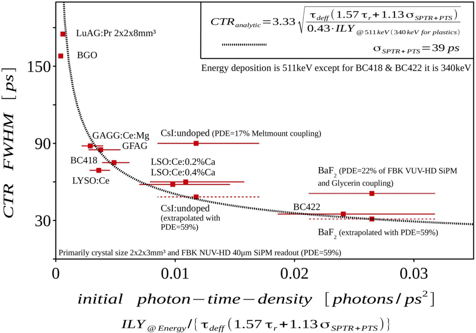
The long aspect ratio crystal dimension imposes inefficiencies in the light transfer of the generated optical photons and time smearing caused by the different photon paths, as the scintillation emission is isotropic. Additionally, the point of gamma conversion in the crystal, the depth-of-interaction (DOI), adds time smearing, because the scintillation photons travel with the speed of light divided by the crystal’s refractive index, and hence, are slower than the 511 keV gammas. For 20 mm long crystals this mismatch equals a minimum time jitter of about 40 ps FWHM in PET and has to be corrected for, if 10 ps should be achieved. Further, the optical photons generated by the scintillation process have a certain time profile, with certain scintillation rise-times τr, decay times τd and intrinsic light yield (ILY). This imposes a theoretical best CTR possible, given by pure photo-statistics CTR2τr ×τd/ILY (Gundacker et al 2016). There are limits for improvements in the ILY given by energy conservation and in τd, by the transition matrix strength of the allowed transitions. Nowadays best inorganic scintillators emitting light in the visible range are not far to reach these limits and improvements over a factor of 10, necessary for 10 ps TOF-PET, are virtually impossible. In figure 2, a summary of the state-of-the-art timing measured with different scintillator materials is shown, readout by the best available SiPMs and high-frequency electronics. It can be seen that with nowadays technology CTRs of 30 ps FWHM are only achievable with fast plastic scintillators (unfortunately not suitable for PET because of their low 511 keV gamma interaction probability), whereas inorganic scintillators perform worse with best values measured of 58 ps FWHM for 3 mm long crystals (Gundacker et al 2019). Even the promising fast cross-luminescence in BaF2 is not sufficient to achieve CTRs below 30 ps, neither if the vacuum ultraviolet (VUV) light could be detected with 59% SiPM photon detection efficiency (PDE). It can as well be seen, that scintillation rise time and SiPM single photon time resolution (SPTR) affect the CTR equally and both have to be improved simultaneously.

Figure 2.

Figure 2.

Measured CTR (y-axis) as a function of the scintillator intrinsic timing capability, given by the scintillation emission initial photon-time-density, on the x-axis. The black dashed line shows an analytic CTR model (Vinogradov 2018) only dependent on the scintillation kinetics and intrinsic light yield (ILY), taking into account the light transfer in the crystal and the SiPM SPTR and PDE. (Gundacker et al 2020).

2. Photo-detector.

The emergence of solid state photo-detectors (SiPMs) was amongst others an important development which made it possible to build commercial PET machines with a CTR of 214 ps (Siemens Biograph Vision) and in laboratory to even reach values of lower 100 ps FWHM with LSO:Ce:Ca of 20 mm length (Gundacker et al 2019). The two most significant parameters of SiPMs to be improved for achieving highest time resolution in PET are the SiPM single photon time resolution (SPTR) and photon detection efficiency (PDE). The PDE of modern devices is reaching values up to 60% (Gundacker et al 2020) for SiPMs with large single photon avalanche diode (SPAD) sizes and, hence, improvements are limited. The ability of the SiPM to time-tag single photons is the one parameter which still can reveal significant progress. This is underlined in figure 3, depicting the CTR performance of different analog SiPMs available on the market, as a function of the SiPM SPTR. Nowadays, the best intrinsic SPTR measured with modern analog SiPMs is 70 ps FWHM (NUV-HD SiPM from Fondazione Bruno Kessler), illuminating the whole 4 × 4 mm2 device (Cates et al 2018, Gundacker et al 2019), still leaving quite some room for improvements, especially in view of prompt photon detection (Cherenkov emission).

Figure 3.

Figure 3.

CTR shown as a function of the SPTR. CTR was measured with 2 × 2 × 3 mm3 LSO:Ce co-doped with 0.4% Ca crystals wrapped in Teflon coupled with Meltmount and normalized, as if all the SiPMs would have a PDE of 59%. Monte Carlo simulations of the CTR were performed for an analog SiPM with high-frequency readout and a hypothetical digital SiPM combining all timestamps via maximum likelihood estimation. The simulations include 7 Cherenkov photons produced. (Gundacker et al 2020).

3. Readout electronics.

The front-end has to keep up with the fast signals provided by the SiPM coupled to the scintillator. In analog systems this means low electronic noise and a very high bandwidth not to lose temporal information of the signal. Recently it has been shown that bandwidths of 1.5 GHz are necessary to benefit of a very high SPTR and fast scintillation emission to achieve best CTRs applying leading edge time discrimination of the amplified signal (Gundacker et al 2019). It further was shown that the electronic noise has to be smaller 1/20 of the single photon signal of the SiPM. These points are especially important for 10 ps systems in the analog case. Here, the digital SiPM, which can time stamp each single photon detected, would give advantages (Fishburn and Charbon 2010, Gundacker et al 2015). The electronic bandwidth would be less critical, only being another parameter defining the SPTR, and not spoiling the time structure of the cascade of scintillation photons detected, which makes any statistical treatment much easier. The vast amount of time stamps could then be combined via maximum likelihood estimation or neural networks to give best possible performance, as was shown in comprehensive simulations (Gundacker et al 2015). In figure 3 the advantages of a digital SiPM and maximum likelihood time estimation over the analog SiPM, for the case of LSO:Ce:Ca can be seen, which underlines the importance of very low SPTR values in the range of 10 ps, which in fact is possible to accomplish with digital SiPMs (Nolet et al 2018a). These simulations also include 7 Cherenkov photons produced on average upon a photo-absorption event in LSO (Gundacker et al 2020).

II. Current and future challenges

Improvements in the CTR, especially to the limit of 10 ps FWHM will only be possible if new ways of scintillation emission can be found, and used properly together with high performance photo-detectors, including the readout electronics.

One possible option could be prompt Cherenkov emission (see also C3) in e.g. BGO with about 17 photons produced on average in the 310–850 nm range upon 511 keV interaction (Gundacker et al 2020). These photons are generated in a time window smaller than 10 ps and could be used as ultrafast time tagger. Recent measurements have shown, that using high-frequency readout and state-of-the-art SiPMs from Fondazione Bruno Kessler (FBK) can achieve a CTR of 159 ps and 277 ps FWHM for 2 × 2 × 3 mm3 and 2 × 2 × 20 mm3 BGO, respectively (Gundacker et al 2020). However, the BGO timing distribution shows long tails, which to a good approximation can be described by a second broader Gaussian from the BGO scintillation, overlapping a thinner Gaussian caused by Cherenkov photons, i.e. the whole CTR distribution can be defined by the sum of two Gaussians G1 and G2: CTR = I1G1 + I2G2, with I1 and I2 being the relative area normalized intensities. For 3 mm long crystals, G1 has 133 ps FWHM containing 52% of the total events (I1) and G2 shows 264 ps FWHM containing 48% of all events (I2). For 20 mm long crystals G1 shows 227 ps FWHM with 45% and G2 shows 795 ps FWHM with 55% of the events. It should be further noted, that by monitoring the detection rate of the incoming photons (signal slew rate in the analog case) it is possible to estimate if the recorded event had good or bad timing, i.e. being part of G1 or G2. Nevertheless, it still has to be proven if in the image reconstruction such complex timing kernels give an advantage in the final SNR improvement. Furthermore, in order to benefit from the prompt Cherenkov radiation in the best possible way, the SPTR of the photo-detector has to be lower than 10 ps FWHM and enough photons have to be detected. However, from simulations it appears that CTRs better 30 ps FWHM are not possible in standard detector arrangements commonly used in TOF-PET, due to the loss of photons and additional time smearing (Gundacker et al 2020). One idea to achieve better timing with Cherenkov photons could be to put a digital SiPM with highest PDE and SPTR on each side of a block detector. However, in order to achieve 10 ps CTR, an exact determination of 511 keV photo-absorption point is indispensable, which might be unfeasible if only the Cherenkov signal is used. Indeed, the triangulation algorithms employed to determine the gamma interaction point are likely to fail, simply because of the too low number of photons detected. Nevertheless, a viable solution to this problem could be the use of semiconductor detectors combined with Cherenkov detection (Ariño-Estrada et al 2018).

Another possibility is to use the promising properties of ultrafast emitting quantum confined systems in form of e.g. CdSe, CsPbBr3 nano-crystals or nano-platelets (Turtos et al 2016, Tomanová et al 2019) (see C5). Indeed, these systems have shown to provide sub-100 ps decay times with theoretically good light yield. Because of the low effective density, these nano-crystals have to be combined in meta-materials with a standard scintillator to form a meta-material. Here, the heavy inorganic scintillator provides the needed energy resolution and gamma stopping power, and the nano-crystals give the ultrafast time tagging. Lower bound calculations presented in figure 4 indeed show that with SiPMs achieving a SPTR of 10 ps FWHM and a PDE of 59% such CdSe nano-platelets ‘only’ have to provide a light yield of 1200 photons/MeV in order to break the 10 ps barrier in TOF-PET. If the system can be produced with sufficient transparency the depth-of-interaction could even be determined solely by the sequence of detected time stamps, using a digital SiPM, which would make it fairly easy to increase the shown 3 mm long crystal case to 20 mm.

Figure 4.

Figure 4.

CTR lower bound of a hypothetical 2 × 2 × 3 mm3 meta-scintillator, if besides the LSO:Ce:Ca scintillation (τd1 = 32.4 ns (95%), τd2 = 7.5 ns (5%), τr = 10 ps and ILY = 32 kph MeV−1) fast emitted photons from CdSe nano-platelets (τd1 = 25 ps (25%), τd2 = 300 ps (75%), τr = 0 ps and ILY = variable on the x-axis) are present. PDE of the SiPM is 59% for all light sources and number of total photons produced (LSO:Ce:Ca + CdSe) is conserved to 32 kph MeV−1.

III. Concluding remarks

New developments in the direction of fully integrated 3D assembled digital SiPMs can push the best achievable time resolution of standard inorganic scintillation processes to values of 40 ps FWHM for 3 mm long crystals. Using the photon arrival time structure (direct and back-reflected photons) the digital SiPM makes it as well possible to reconstruct the DOI out of the detected time stamps only, which is indispensable in order to reach such CTRs with longer crystals of e.g. 20 mm. Although standard inorganic scintillation processes are likely not be able to provide a TOF resolution of 10 ps FWHM, they may provide time resolutions of ~40 ps FWHM, which would be the starting point of recording true space points in full body PET. The only way possible with nowadays technology to achieve 10 ps seems to be the use of ultrafast nano-crystals assembled in efficient meta-materials, together with photo-detectors delivering SPTRs of 10 ps FWHM and high PDE (>60%). In the future, an additional integration of the photo-detector in the meta-material would form a new class of functional and active super-material for gamma detection and far beyond.

C2. Perspectives on using inorganic scintillators for fast timing applications

Etiennette Auffray

I. Status

The time resolution of a detector based on inorganic scintillators is a measure for the precision of the time stamp that can be attributed to the detection of a particle. The time resolution depends on the shape and the amplitude of the light signal produced by a particle in an inorganic scintillator. The intensity of the scintillation light as a function of time is in general described using a bi-exponential expression (Shao 2007):

I(t)=I(0)et/τd(1et/τr) (1)

with τr being the scintillation rise time and τd the scintillation decay time. I(0) is proportional to the total amount of light produced in the scintillator. Convoluted with the time between the generation of each photon and its conversion into a photoelectron in the photo-detector, equation (1) can also approximately describe the rate of photoelectrons above the detection threshold as a function of time.

The stochastic nature of the photon generation and conversion processes leads to fluctuations impacting the time resolution of the detector system and the initial photon rate is directly correlated by:

CTRτrτdNPhp (2)

with NPhP being the number of detected photo electrons. An accurate timing resolution hence requires inorganic scintillators with a high light yield and a short fall-off time (τd), as in first approximation the photon density is given by LY/τd. The rise time τr in addition delays the emission and the conversion of the first produced photons, increases their time jitter and consequently reduces the time resolution of the scintillator. This is a result of the cascade relaxation mechanism of the hot electron-hole pairs produced by the interacting ionizing radiation with the crystal material, before the transfer to the luminescent centres of the scintillator. The entire relaxation process is stochastic and hence leads to statistical fluctuations in the generation of the first scintillation photons.

Typical CTR values for widely used standard scintillators with a dimension of 2 × 2 × 20 mm3 are currently in the order of 100 ps or higher. The best CTR value obtained so far for a 2 × 2 × 20 mm3 is 98 ps for LSO co-doped Ce, Ca (Gundacker et al 2019).

Over the last years, a significant R&D effort has been carried out within Crystal clear Collaboration (CCC) and several European projects initiated by CCC such as TICAL, COST ASCIMAT, Intelum (TICAL, COST Action TD1401 (FAST), ASCIMAT, Intelum) and has shown that standard scintillators are unlikely to reach the target of 10 ps coincidence time resolution at 511 keV. Indeed, today’s bests scintillators in terms of light yield do not exceed 100000 ph Mev−1 (Dorenbos et al 2010) and the fastest decay time observed is of the order of 10–20 ns, so the density of photons per ps for 511 keV cannot be higher than 5 combined with the delay introduce by rise time. This sets an intrinsic limit to the achievable coincidence time resolution of a scintillator to ≳50 ps FWHM.

A few approaches have been identified to provide a photon time density in the leading edge of the scintillation pulse compatible with a 10 ps CTR target. A strong effort must therefore be carried out along the following lines:

  • Improvement of the timing performance of existing scintillators to get highest light yield, and/or shortest rise and decay time.

  • Study of materials with fast emission process such as cross-luminescence, hot intra-band luminescence, Cerenkov

II. Current and future challenges

1. Enhanced understanding of the charge carrier relaxation to luminescent centres and identification of possible ways to improve the efficiency of the energy transfer to luminescence centres.

The scintillation process itself consists of a set of complex steps from hot electron-hole pair creation to the energy transfer to the luminescence centre (Vasil’ev 1999). The latter step is characterized by an increased probability for electrons or holes to be trapped due to crystal defects (ions vacancies, dislocations, local lattice disorder, etc) even for high purity material, which can impact the optical and timing properties of the crystal.

Decreasing the rise time requires research activities in two directions:

  • maximal suppression of shallow traps, which are responsible for delaying the capture of electron-hole pairs by the luminescent centre in the crystal

  • fastest possible exciton direct relaxation or trapping by the luminescent centres.

Attempts to overcome this limitation are to use specific doping in intrinsic scintillators or co-doping activated scintillators is a promising way to increase the photon time density in the leading edge of the scintillation pulse. The objective of specific doping/co-doping is to compete with charge carrier traps allowing in some cases the suppression of afterglow, in other cases the improvement of radiation hardness or a faster energy transfer to the emission centre and therefore reducing the rise and decay time. This has been successfully achieved in the last years by the use of co-doping with aliovalent ions for cerium doped oxide based scintillators such oxy-orthosilicates (LSO, LYSO, YSO) with calcium co-doping (Spurrier et al 2008) or garnet material such LuAG, YAG and GAGG with Magnesium co-doping (Nikl et al 2014). Co-doping reduces the rise time down to a few tens of picoseconds (Gundacker et al 2018) and the decay time to a few tens of ns without significantly impacting the LY. Both for oxy-orthosilicates and garnet material a significant improvement for the coincidence time resolution has been observed from only Ce doped to co-doped Ca/Mg (Lucchini et al 2016, Gundacker et al 2018). This strategy should be extended to a larger number of scintillators.

2. Identification and characterization of materials with a fast emission process such as hot intra-band luminescence, cross-luminescence and Cerenkov (see sections C1,C3), nanomaterial (see sections C1, C4).

In view of the intrinsic difficulties in improving the time resolution of standard scintillator materials below 100 ps, further strategies need to be investigated.

The complexity of scintillating process from the creation of hot electron pairs to scintillation is one of main reason for the limitations of time resolution in standard scintillators. The optimal way to overcome this limitation would be to have a radiative relaxation mechanism for non-thermalized charge carriers, i.e. in the first picosecond following gamma excitation of scintillating materials. In some materials, this mechanism (hot intra-band luminescence) can occur when the density of states has some specificities, like a gap in the bottom of the conduction band or top of valence band. Intra-band luminescence is due to radiative transitions of hot electrons or holes between the sub-levels of the conduction or valence band respectively. It has characteristic decay time of about 1 ps with a relatively flat emission spectrum in the visible region (Omelkov et al 2018).

Hot intra-band luminescence has been studied on a large number of materials from the group of complex halides and oxides. The light yield was found to be rather small, the best yield obtained for CsI was 33 ph MeV−1 (Omelkov et al 2018). Though the exclusive use of intra-band luminescence materials with such a low light yield is not suitable to get time resolution close to 10 ps, combining such scintillators with very fast emission providing prompt photons with other dense materials with high light yield can improve the CTR (see sections C1, C4). Materials with low phonon energy should be investigated due to the competition between phonon relaxation and fast radiative processes within an electronic energy band. It is assumed that the specific band structure and in particular the presence of energy gaps in the density of states in the valence and conduction bands, can reduce the probability of electron-phonon relaxation, leading to an increase of the hot intra-band luminescence yield at the expense of a slight increase of the emission decay time. Studies have to be carried out using theoretical tools including electronic band structure calculations to identify material parameters to obtain a higher yield of intra-band luminescence emission.

Another strategy to follow is to search for materials with a high quantity of delocalized electrons able to radiatively recombine quickly with holes, as it is the case in cross luminescence material or wide band gap, direct heavy semiconductors. In this case a fast emission process with relatively high number can occur.

Cross-luminescence is due to radiative recombination of electrons from the valence band with the holes in the uppermost core band (Van Eijk 1994). It has a slower emission than intra-band luminescence with a sub nanosecond decay time. On the other hand, the light yield can be relatively high (e.g. 1400 ph MeV−1 for BaF2 (Van Eijk 1994)). The maximum of the emission spectrum is in general in the deep UV region at around 150 nm-250 nm (Van Eijk 1994). For this part of the spectrum the small quantum efficiency of photo detectors puts severe limitations for exploiting these photons for timing purposes. However, with the recent development of deep UV sensitive photo-detector and in particular SiPM for noble gas liquid scintillator for dark matter, cross luminescence materials became again more interesting. Using current state-of-the-art VUV SIPM, a CTR of 68 ps was obtained using a 2 × 2 × 3 mm3 BaF2 sample, compared to a CTR of 60 ps with a co-doped (Ce, Ca) LSO of the same size LSO (see figure 2 in section C1). The todays state-of-the-art PDE of 25% in the deep UV region leads to the assumption that this CTR can be improved in the future with improvement of photo-detectors’ PDE.

Cross-luminescence has been observed mainly in halide materials with Ba, Cs, K, Rb cations in binary and complex composition (Van Eijk 1994). For some materials a near-UV Cross-luminescence emission (205–300 nm) has been observed (Van Eijk 1994). As for intra-band luminescence band structure calculations is needed to identify material with complex valence bands, which could exhibit cross luminescence transitions not only in UV-VUV but also in the visible region.

Therefore, the investigation of long-wavelength cross-luminescence emission together with the optimization of the PDE in NUV photo-detectors and optical gluing are a route forward to a time resolution of 10 ps.

III. Concluding remarks

Although standard scintillators are unlikely to reach the target of 10 ps coincidence time resolution at 511 keV, several ways to improve the time resolution towards 10 ps are available through engineering the band structures of existing materials and further investigations, thanks to novel characterization techniques now available, of fast emission process existing in several materials.

C3. Perspectives on using Cherenkov light for fast timing applications

Peter Križan

I. Status

1. Introduction.

The annihilation gamma rays, used in PET, interact with the crystals serving as gamma stopping material via the photoelectric effect or Compton scattering. In both processes, a fast electron is emitted, the energy of which is in part converted to scintillation light. Traditionally, all information in PET is subsequently derived from the detection of this light. However, even before the electrons are slowed down (on a time scale of 1 ps) and scintillation photons begin to be emitted (on a time scale of 100 ps), another source of information is available. This is the Cherenkov light, produced while the electron velocity is greater than the speed of light in the gamma stopping material. In effect, the Cherenkov photons are produced promptly, and although only about 10–17 photons are expected from a 511 keV gamma in materials, suitable for PET detectors, their potential for providing an excellent timing looks very promising.

Using Cherenkov light in PET was first discussed in (Ooba et al 2004), where silica aerogel was considered as the radiator of Cherenkov light, but due to the very low density of such material the detection efficiency for 511 keV gammas would be very low. When lead glass was employed as the radiator material in combination with micro-channel plate photomultiplier tubes (MCP PMTs) as photo-detectors, a 170 ps FWHM coincidence time resolution was reported (Miyata et al 2006). Another early experimental demonstration was the comparison of the properties of light produced by 511 keV gammas in doped (scintillating) and un-doped (non-scintillating) LuAG crystals (Lecoq et al 2010), where a 250 ps FWHM time resolution was measured between two small, un-doped crystals in coincidence.

2. Proof-of-principle.

One material, already used as Cherenkov radiator in calorimetry in particle physics experiments (Mao and Zhang 2010), is the lead fluoride (PbF2) crystal. Its gamma stopping power is higher than that of scintillators commonly used in PET (1.06 cm−1 compared to 0.87 cm−1 for LSO and 0.96 cm−1 for BGO), has excellent optical properties for transmission of Cherenkov light (good transparency down to about 250 nm), does not scintillate, and has a low price (1/3 of the BGO scintillator (Mao and Zhang 2010)). Using 15 mm thick PbF2 crystals, which are comparable in gamma stopping power to 20 mm of LSO, and MCP PMTs, a coincidence time resolution of 95 ps FWHM was demonstrated (figure 5) (Korpar et al 2011, 2012). With a thinner, 5 mm thick crystal, a considerably faster response can be achieved: 71 ps FWHM in the same set-up (out of which 50 ps are attributed to the MCP-PMT response), and 47 ps FWHM with a faster MCP-PMT by Ota et al (2019a). A further improvement to 30 ps FWHM was obtained by integrating a 3.2 mm thin lead glass gamma converter into the MCP-PMT instead of the MCP-MPT window (Ota et al 2019b).

Figure 5.

Figure 5.

The coincidence timing distributions obtained with 15 mm thick PbF2 crystals with black painted surfaces (Korpar et al 2011).

3. Cherenkov light detection with SiPMs.

However, using MCP PMTs as photo-detectors has the drawbacks of high cost and limited efficiency. Only 6% single side detection efficiency was reported (Dolenec et al 2016). For this reason, silicon photomultiplier (SiPM) photo-detectors were considered as light sensors, as they have very high photon detection efficiencies. In combination with a 5 × 5 × 15 mm3 PbF2 crystal, a coincidence time resolution of 297 ps FWHM was measured, while a single side detection efficiency of over 25% was reached (Dolenec et al 2016). Recently, a Cherenkov PET module, composed of 4 × 4 arrays of 3 × 3 × 15 mm3 PbF2 crystals and SiPMs, was assembled, and a very good uniformity and an average detection efficiency of 35% was experimentally demonstrated (figure 6) (Dolenec et al 2020).

Figure 6.

Figure 6.

The gamma detection efficiencies measured by all channels of the Cherenkov detector module (Dolenec et al 2020).

II. Current and future challenges

An interesting way to maximise light extraction efficiency, and therefore reduce multiple bouncing, for photons touching for the first time the light extraction surface could be achieved by using photonic crystals (Salomoni et al 2018).

A possible approach to achieve fast timing without sacrificing gamma stopping power or Cherenkov photon detection efficiency is to use a multi-layered detector approach. Simulations of a three-layer PbF2 Cherenkov PET detector with a total thickness of 15 mm, comprised of 5 mm thick individually read-out crystals, indicate that with an ideal photo-detector time response a 22 ps FWHM coincidence time resolution is possible; even with 100 ps of photo-detector time response included, the reconstructed image quality is comparable to that of a standard LSO scanner (Consuegra et al 2020). Note also that while 100 ps is the present state-of-the-art for the most recent SiPM generation, a large effort is under way to improve this value with a 10 ps target; this is in particular the subject of the EU funded project PHOTOQUANT (attract-eu.com).

Another interesting approach is to combine scintillations with Cherenkov light to improve the timing performance. This hybrid method has been investigated with LSO and BGO crystals (Lecoq et al 2010, Kwon et al 2016, Brunner and Schaart 2017).

III. Concluding remarks

The Cherenkov radiation is currently the first prompt light production mechanism, for which realistic and practical PET detectors have been experimentally demonstrated. Due to the limitations of current photo-detector technology, it has proven difficult to achieve both a good detection efficiency and TOF resolution at the same time. However, initial simulation studies suggest that the reconstructed image quality for a PbF2 Cherenkov TOF PET scanner can be at least comparable to current clinical systems. The significantly lower material price of the PbF2 radiator compared to that of LSO or BGO scintillators therefore opens a possibility to reduce the cost of PET scanners and make this modality more widely available. The low price, the excellent TOF resolution and the possibility to reduce the parallax error with a multilayer detector makes the Cherenkov detectors especially suited for the recently developed total-body scanners (Cherry et al 2018), where the price of materials needed to cover the whole length of human body can be prohibitive.

C4. Perspectives on using nano-scintillators for fast timing applications

Rosana Martinez Turtos

I. Status

The emergence of new scintillating materials driven by the development of nanotechnology and advanced nanofabrication techniques has opened the doors to consider fast emitting nano-semiconductors as effective time taggers for 511 keV gamma detection (Turtos et al 2019b). Nano-crystals semiconductors having a size dependent band-gap and therefore tunable opto-electronic properties exhibit a very peculiar excitonic-multiexcitonic dynamic able to combine sub-1 ns radiative recombination times with an exceptional suppression of nonlinear luminescence quenching (Moreels 2015), which is critical for fast timing applications.

Among all the different nano-crystal geometries going from quantum dots (3D) to nanowires (2D), nano-platelets (NPls) with 1D quantum confinement of charge carriers present one of the most interesting scintillating features at room temperature: red-shifted bi-excitonic emission with high binding energies. This ultrafast emission, while not instantaneous, present characteristic radiative lifetimes of around 4 times smaller than the exciton’s decay time and could offer a higher photo-emission yield in comparison to Cherenkov or hot intra-band emission with a maximum number of around 20 photons per gammas interaction. First spectroscopy studies of the bi-excitonic emission have been previously conducted using CdSe-based NPls of 4 monolayers (4 ml) under amplified laser and x-ray excitation (Grim et al 2014, Turtos et al 2019b). Furthermore, the one-dimensional quantum well potential allows for a considerable suppression of Auger recombination processes, a collective phasing of dipoles over many unit cells leading to a giant oscillator strength transition (Feldmann et al 1987) and Förster resonance energy transfer (FRET) inter-plate mechanisms with picosecond lifetimes (Rowland et al 2015).

In respect to the different fabrication and synthesis methods, wet-chemistry has outstanding merits due to its relatively easy, cheap and scalable production techniques, reaching very narrow size distribution and highly controllable shape, aspect ratio and core/shell hetero-structures. Another interesting fact of solution-processed nano-crystal is the presence of organic ligands guaranteeing surface passivation and forming a hybrid organic-inorganic nanoparticle compound suitable for surface chemistry manipulation. In this regard, a very interesting family of lead halide XPbBr3 perovskites colloidal nano-crystals has emerged due to their high defect tolerance (Kovalenko et al 2017), usually above band gap, and therefore bright luminescence. Their application has proven to be disruptive in the field of photovoltaic cells and the possibility of synthesizing CsPbBr3 in the shape of NPls offers exciting and new opportunities in the field of fast timing research (Tomanová et al 2019).

All the features presented above are in well alignment with the implementation of NPls as a fast radiation detector able to break the time resolution limit in particle detection. However, their nano-scale sizes impose several limitations in terms of energy deposition per platelet and their small Stokes shift introduces self and re-absorption issues that are to be minimized when building large scale sensors. In view of this, a new concept for particle detection using hybrid pixels have been implemented, in which a high-Z inorganic scintillator is efficiently combined with nano-crystal-based built-up layers able to perform as time taggers by increasing the number of fast photons emitted per 511 keV excitation (Turtos et al 2019a). In this sampling approach an energy sharing scheme allows to add prompt photons to the standard scintillating signal, a solution suggested in one of the first studies on how to reach 10 ps time resolution (Gundacker et al 2016). A depiction of the sampling pixel approach that allows for the energy sharing scheme between bulk and nano-scintillators is shown in figure 7.

Figure 7.

Figure 7.

511 keV gamma interaction in a sampling pixel composed by alternating layers of a high-Z and a fast, nano-scintillator (adapted from (Turtos et al 2019a)).

The CTR achieved with the first generation of sampling pixel detectors is shown in figure 8 together with state-of-the-art bulk materials used as the gamma stopper.

Figure 8.

Figure 8.

CTR values achieved with a first generation of sampling pixel detectors when coupled to the best photo-detector and electronic readout available (Grim et al 2014, Turtos et al 2019a, 2019b).

So far, CdSe-based NPls has been used in the form of drop-casted films as a direct coating on the surface of high-Z materials such as LYSO. This primitive deposition technique enabled the first assembly of several sampling pixels for a first-time characterization using 511 keV gammas. However, it relies on highly quenched-ligand’s washed nanoparticles with no hosting medium able to properly transfer energy among emitting centres. Therefore, modest light yield values at the level of 200 ph MeV−1 have been measured with few micrometres thick CdSe/CdS core-crown films (Turtos et al 2019b) and low weight concentration CdSe/CdS in polystyrene nano-composite layers up to 0.5 mm thick. Despite the low light output and the loss of index light guiding within the pixel, the timing obtained is at the level of state-of-the-art values, leaving a rather large room for optimization.

II. Current and future challenges

Enhancing the number of prompt photons available for 511 keV gamma time-tagging constitutes one of the corner stones in the implementation of nano-semiconductors as fast radiation detectors. A clear example is seen when using BGO, a Cherenkov emitter, in combination with CdSe/CdS NPls as shown in figure 9. A prompt peak with a yield four times higher than standard Cherenkov emission can be seen when measuring the rise time of a BGO + CdSe sampling scintillating pixel in a time correlated single photon counting (TCSPC) setup that uses 511 keV gammas as excitation source.

Figure 9.

Figure 9.

Rise time of CdSe-BGO sampling pixel measured under 511 keV gamma excitation in a TCSPC setup for the average type of event, including Compton.

Optically separating the standard and fast photon-emitting phase would preserve the high-Z scintillator performance meanwhile adding the prompt photons to the standard signal. This will avoid the loss of index-light-guiding when coating high-Z inorganic scintillators with semiconductor NPls, which in general present locally higher index of refraction. In this direction, we would need to advance in the fabrication of at least 100 μm thick built-up fast nano-crystal based layer able to perform as time tagger for 511 keV gamma detection. The critical parameters for the performance of the nano-scintillating layer can be described as follows:

  • have the minimum thickness allowing the emission of at least several hundreds of prompt photons from the energy deposited by the photoelectric recoil electron traversing this layer.

  • be as transparent as possible to allow these prompt photons to propagate to the photo-detector.

  • have an overall density as high as possible to also allow direct gamma ray conversion in this layer and to keep the stopping power and the photo-fraction of the meta-pixel as close as possible to a bulk scintillator of the same size.

In addition, research needs to be developed in order to move towards larger size pixel sensors where a DOI correction is to be integrated with the event identification algorithm. A feasibility study for the production of nano-scintillator based hollow core photonic fibres, where light emission and transport occur in different mediums is also at the top of the solutions for the light transport bottleneck.

1. Enabling technologies.

The chemical path allowing highly loaded nano-composites up to 60% in weight concentration is already in place for CdZnS/ZnS quantum dots embedded in polyvinyl-toluene (Liu et al 2017), reaching transmission values up to 80%. In this direction, a scale-up in weight concentrations of CdSe-based NPls up to 10% is needed in order to harvest close to 100% of the energy deposited in the host matrix via FRET or exciton diffusion. In this regard, the ligand surface modification of NPls allowing for a mono-disperse distribution of covalently bound nano-emitters in polystyrene or polyvinyl-toluene needs to be developed.

A FRET mechanism for a non-radiative wavelength shifting processes yielding a sharp rise time and a transmission improvement is available in NPls. For this, 4 and 5 monolayers CdSe NPls (Rowland et al 2015) are potential candidates with FRET in the 6–23 picosecond range for inter-plate transfer.

Core/shell CdSe/CdS hetero-structures offering robust surface passivation and allowing to shift the emission from 515 nm towards 550 nm could provide a perfect spectral match with scintillators such as the family of aluminium garnets. Emission spectral match between bulk and nano-scintillators contributes to the overall transparency of the sampling pixel. Among these, GAGG:Ce co-doped with Mg2+ presents very good timing characteristics (Gundacker et al 2020) and could be a potential material to replace LYSO in the hybrid approach. Garnets ceramics are also manufactured through an innovative 3D printing process, in which complicated structures with 100–200 μm features are built-up (Dosovitskiy et al 2017).

Advanced 3D printing techniques using costumed-made nanoparticles-based ink would allow to cover a relatively large area with a 4–5 monolayers of a fast scintillating material.

Another technique suitable for the nanofabrication of one dimensional semiconductors is metal-organic vapour-phase epitaxy (MOVPE), which allows for a layer by layer deposition of multiple quantum wells. Multiple hetero-structures composed of InGaN/GaN can be grown on a sapphire substrate (Toci et al 2019), which contributes to the mechanical stability of the scintillating layer. The replacement of the dead sapphire layer by state-of-the-art active materials such as LYSO or BGO could lead to a fully integrated nano-scintillator with a standard and fast scintillating phase. However, finding a technological efficient way to overcome the crystalline lattice mismatch between GaN and state-of-the-art scintillators is still a challenge. Currently, the maximum thickness obtained for this type of samples is limited to 10 μm (Toci et al 2019), which set constraints in the amount of energy deposited in the active region.

III. Concluding remarks

Move towards a layer-by-layer built meta-scintillator with a homogeneous energy deposition scheme upon 511 keV gamma detection. Bridging the gap between the nano-world and bulk material will lead to a new generation of scintillators enabling a technological breakthrough in particle detection.

C5. Perspectives on LAr and/or LXe scintillators for fast timing applications

Dominique Thers

I. Status

Since more than 50 years, there is a growing interest in identifying pure noble gases intrinsic liquid scintillators, including γ-ray cameras, as new generation particle detectors (Aprile and Doke 2010). Three important properties that are common to those type of detectors are: the high scintillation light yield due to the formation of excited dimers which is also at the origin of the fast scintillation decay time, the inert chemistry allowing for the direct immersion of photo-detectors with a quite perfect optical coupling and finally, certainly the most important, the presence of a permanent liquid phase at thermodynamic equilibrium allowing for a complete coverage of large monolithic volumes. Furthermore, liquid xenon (LXe) is also well motivated by a ‘quite easy’ cryogenics and by the ultra-low intrinsic radioactivity that make it easily scalable. This provides a cheap solution for low dose total-body imaging detection devices that require the use of tons of liquid noble gases.

Despite this impressive list of features, the detection of γ-rays is limited by electron density of the target. It is here fundamental to underline that for all liquid noble gases a quite large depth of interaction is mandatory: typically, around 3 cm or more for LXe and at least 6 cm or more for LAr. In addition, a dominant fraction of events will undergo through Compton scattering (Aprile et al 2008) allowing for an efficient tracking, like it is under development with the XEMIS project (Gallego Manzano et al 2015), but also strong limits in case of limited volume for the calorimetry point of view.

Excellent time resolutions have been firstly measured by Lavoie in 1976 (Lavoie 1976); later on, key researches based on prototyping have progressively reached better and better performances. It is worth to mention two major past milestones: the first nanosecond time coincidence windows obtained with 511 keV photons (Chepel et al 1997) and the proof of concept for LXe time-of-flight reporting 260 ps (FWHM) time resolution (Doke et al 2006).

II. Current and future challenges

Until now, fast timing resolutions with LAr and LXe detectors have constantly increased thanks to technological progresses without reaching asymptotic intrinsic limits for 511 keV γ-rays. With prototypes design combining light and charge measurements (Amaudruz et al 2009), LXe PET camera benefit from both the excellent depth of interaction measurements and the exceptional time resolution (Miceli et al 2012). Since few years, photo-detectors quantum efficiency is now quite impressive in VUV region, reaching more than 20%/40%, respectively with LAr/LXe scintillation photons. Challenges for next camera designs are then well established, with a roadmap focusing also on the light detection coverage benefiting from new thin and compact devices working at cryogenics temperature: SiPM/MPPC (Ogawa 2018).

LXe is also an excellent Cherenkov radiator target (Gomez-Cadenas et al 2017) for high energy electron escaping photoelectric 511 keV γ-rays interaction. For 10 ps time resolution challenge, the detection of this additional light emission component combined with fast CRT photo-detectors and very low jitter electronics could lead to impressive results (Gomez-Cadenas et al 2016).

III. Concluding remarks

Intrinsic scintillators based on liquid noble gases are very well suited for gamma rays detection on large volumes; their past developments demonstrated progressively and experimentally their exceptional characteristics for high energy, rare events or neutrinos physics experiments.

In parallel, PET images quality did impressive progresses benefiting from the large interest of the community. Investments have been successfully made to develop cameras with better DOI measurement achieving a few mm FWHM (Yoshida et al 2017), with total axial field-of-view reaching 2 m (Badawi et al 2019) or with TOF-PET scintillators and associated electronics for fast coincidences, which amounts a CTR of 215 ps FWHM with a 26.3 cm axial field-of-view (van Sluis et al 2019). Thanks particularly to LXe cameras properties, next generations of PET camera based on solid scintillators would have to face a tough opponent able to present a full set of impressive performances combining simultaneously large design, ultra-precise DOI capability and also the presence of a fast TOF (benefiting or not from Cherenkov light characteristics). Giant cameras containing liquid noble gases should then play a key role for revisiting the PET paradigms like very fast or ultra-low dose imaging techniques.

Acknowledgments

The author wish to thank all her colleagues from Crystal Clear Collaboration and acknowledge the support of several European projects: ERC grant (TICAL, agreement 338953), the COST Action TD1401 (FAST), the European TWIN project (ASCIMAT grant agreement 690599), European RISE project (Intelum, grant agreement 644260).

The author would like to acknowledge the support received by TICAL, ERC Advanced Grant, PI Paul Lecoq, Grant No. 338953.

Phys Med Biol. 2020 Oct 22;65(21):21RM01.
Edoardo Charbon

D. Photo-detectors and readout electronics

D1. Perspectives on photo-detectors

I. Status

With the rise of analog silicon photomultipliers (A-SiPMs) in the late 1990 s, it has become clear that photomultiplier tubes could eventually be replaced by a solid-state solution (Dolgoshein 2003), (Collazuol 2012), (Schaart et al 2018). This trend has continued in the 2000 s, while the emergence of digital SiPMs (D-SiPMs) have done little to stop the consolidation of the trend (Frach et al 2009). In fact, A-SiPMs have in general shown better dark count rate (DCR) and photon detection efficiency (PDE) if compared with D-SiPMs. This is due to the choice of optimized silicon technologies and the lack of circuitry between single-photon avalanche diodes (SPADs), despite advanced methods to suppress noisy SPADs (with loss of PDE) and to reduce the effects of higher median DCR on gamma detection.

Multi-channel digital SiPMs, sometimes called multi-digital SiPMs (MD-SiPMs) (Mandai et al 2014), (Braga et al 2013), though requiring complementary metal oxide semi-conductor (CMOS) technologies (the presence of both PMOS and NMOS transistors), hold the promise to use circuit techniques to counter higher DCR and reduced PDE. Though, current implementations have yet to deliver this promise to its fullest and the community is often preferring A-SiPMs mostly for their simplicity and ease of use, despite the need of external amplifiers and time discriminators. Indeed, D-SiPMs and MD-SiPMs offer in situ time-to-digital conversion, higher granularity of measurements, which, in combination with statistical algorithms, ensure higher timing resolution predictability.

In the second half of the 2010 s, the image sensor industry has launched several pilot projects to achieve mass-produced 3D ICs, including low-cost packaging for optical sensors. This trend is gradually leading to hybrid SiPMs, i.e. a combination of A-SiPMs or arrays of A-SiPMs, even in non-Si materials, like Ge and GaAs/InP on the top tier and advanced electronics implemented in CMOS technology nodes with <45 nm feature size in the bottom tier. These solutions could be a good compromise enabling the performance advantage of A-SiPMs, in situ time-to-digital conversion of D-SiPMs, and granularity/flexibility of MD-SiPMs (Mata Pavia et al 2015). A disadvantage is the increase in complexity to control these systems and the potential heat transfer from bottom to top tiers, thus potentially increasing DCR and jitter. Moreover, the cost of this technology is still high if compared with simpler 2D CMOS (or custom) technological nodes.

More recently, next to improved detectors, there has been growing interest in computational techniques to enhance reconstruction results. In computational photography, deep learning and artificial neural networks have taken over the field enabling drastic improvements in several applications. Neural networks (NNs) and other deep learning techniques could be used in PET/SPECT related applications, where jitter could be reduced by predicting gamma depth of interaction, energy, and photon order (Venialgo et al 2013, Geoffroy et al 2015, Berg and Cherry 2018). NNs can be implemented efficiently in the digital domain using convolutional NNs and spiking NNs either in application-specific integrated circuits (ASICs) or in field programmable gate arrays (FPGAs) (Berg and Cherry 2018). We envision the increased use of these techniques near the sensor and also near the reconstruction engine.

II. Current and future challenges

One of the conditions to implement these and even more advanced functionality is the availability of even more advanced 3D integration and/or multi-layer 3D-stacking. Sony has already experimented with 3-tier stacking (Mabuchi 2011). However, we expect this trend to accelerate further with 4-tier and higher to be developed in mass-production in the next few years. We expect 4-tier technology to be developed in the 2020 s with the improvement of current technology and the deceleration of feature size reduction. This trend is mostly an economical one, related to the exponential increase of the costs expected for <3 nm CMOS technology nodes. In fact, we expect that in the mid 2020 s, the cost of 3D IC will become comparable if not lower than that of equivalent 2D chips. One of the most important challenges though will be the power transfer and important breakthroughs will be needed to ease this problem, such as cooling trenches and fluid canals in through-silicon vias (see figure 10).

Figure 10.

Figure 10.

New technologies in detectors for PET/SPECT systems. (left) backside-illumination (BSI) detectors on a top layer combined with processing in the bottom layer in a 3D IC configuration: cross-section; (centre) photon detection probability in several BSI detectors and 3D ICs: note the different excess bias voltages (aka overvoltages) used; (right) photomicrograph of an array if single-photon avalanche diodes (SPADs) from the backside, while the bottom layer (not visible) is 3D-stacked in (Mata Pavia et al 2015, Lee et al 2018): the bottom layer is implemented in a more advanced CMOS technology node, thereby enabling extensive computations in situ.

Temperature control in photo-detectors has become important in recent years, not only for DCR reduction but also to operate SiPMs in liquid scintillators, such as liquid Ar and Xe. The demonstration of cryogenic SPADs and SiPMs at 77 K has shown that PDE remains practically unchanged but electronics needs to operate at room temperature (Acerbi et al 2017, Patra et al 2018). Recently, the emergence of cryogenic electronics could potentially make cryo-SiPMs much more compact and scalable, especially whenever cryogenic coolant is already present.

III. Concluding remarks

In summary, photo-detectors are developing along several axes, involving new detecting materials, 3D IC technology, cryogenic operation, and deep learning. We believe these trends will lead to better time resolution, ultimately achieving 10 ps at lower DCR and comparable or better PDE. All these improvements are likely to be achieved with solid-state or MEMS photo-detectors, sensitive to the extended visible range but also potentially deep and extreme UV, as well as mid infrared.

D2. Design criteria for fast timing readout electronics

Joao Varela and Christophe de La Taille

I. Status

In the race for picosecond timing detectors, readout electronics plays a crucial role, in particular for small signals or large number of channels, which is a general trend in such detectors. This is resulting in the generalized use of ASICs, which helps a lot on the performance thanks to their high internal speed, but at the expense of limited power dissipation and thus larger noise. The timing performance is affected by the electronics in three places: jitter due to electronics noise, error in time walk correction and time-to-digital converter (TDC) resolution, summarized with the formula below:

σ=tr/SNR+σ(Timewalk)+σ(TDC) (3)

which is dominated by the first term (jitter) for small signals. Observing that the rise time tr is inversely proportional to the bandwidth (1/BW) whereas the electronics noise scales as the square root of the bandwidth (√BW), it would seem that the jitter can be minimized by using front-end electronics as fast as possible. However, this is disregarding the fact that most sensors used in timing detectors (Si diodes, APDs, LGADs, SPADs, SiPMs, see table 2) are current sources with capacitive impedance. At very high frequency (GHz), it is almost impossible to avoid that the detector current be integrated on the sensor capacitance, therefore the signal rise time is proportional to the current duration and not really to the current rise time. Therefore, the preamplifier rise time, even with infinitely fast electronics is simply the current duration. Using faster preamplifiers then only increases the noise without gaining on the preamp rise time. It can be shown analytically that the optimum electronics rise time tr is equal to the current duration td (FWHM). It should be emphasized that the bandwidth for the electronics concerns not only the preamplifier but also the discriminator. A rise time in the range 0.1–1 ns corresponds to bandwidths of 350 MHz–3 GHz.

Table 2.

Comparison of the key parameters determining the jitter performance for different sensors. Capacitance (Cd), current duration (tr) and charge (Q) allow to calculate the expected jitter with equation (4), which can be compared to typical measured performance.

Sensor area mm2 capacitance Cd (pF) current duration tr (ns) Charge Q (fC/MIP) expected jitter ps rms measured jitter
Si pixel 0.01 0.1–1 1–5 1–4 4–90 300–3000
PIN diode 1–10 1–10 1–5 1–4 40–900
APD 1–10 5–50 1–5 5–50 10–400 100–1000 (Bornheim et al 2017)
LGAD 1–5 1–5 0.5–1 5–50 3–20 20–200 (Cartiglia etal 2017, de La Taille et al 2018)
PMT 100–10 000 5–10 1–5 100–1000 1–5
SiPM 1–5 50–500 0.1 10–100 3–300 50–500 (Gundacker et al 2019)
RPC 100–500 0.1–5 1000 3–30 50–500

Several preamplifier configurations have been used by different groups, mostly were transimpedance amplifiers (charge or current preamplifiers) or voltage amplifiers (RF or broadband amplifiers). However, at very high frequency they exhibit similar behaviour and it can be shown that the jitter can be expressed as:

J=tr/SNR=enCdtd/Q (4)

where en is the noise spectral density of the input amplifier, Cd is the total capacitance at the input, td is the current duration (FWHM) and Q the charge delivered by the sensor.

It can be observed that the sensor determines three of the four terms in the equation (Cd, tr and Q).

Therefore detectors that produce large charge on a small capacitance with a short current duration are performing best. Also sensors with gain are also better. Hence SiPMs offer an excellent potential as shown in table 2, which compares these parameters from different sensors and the expected jitter. The term due to electronics depends essentially on the power that can be allocated to the preamplifier stage. A usual rule of thumb gives en ≈ 1/√I(mA) in nV/√Hz. As it only scales with the square root of the current, it is usually more efficient to play with the sensor capacitance.

II. Current and future challenges

The applications using LYSO crystal associated to SiPM are an exception to the considerations above given the very long decay time of the LYSO scintillation light when compared to the low time resolution aimed at. There are about three orders of magnitude difference in the two times scales involved, namely about 40 ns of the LYSO light decay time and ~10 ps time resolution. In this special case, good timing is possibly only by taking profit of the large number of photoelectrons per event (several thousand) and measuring the time of arrival of the first few photoelectrons. This requires a very fast amplifier capable to follow the rising edge of the single-photon avalanche in a SPAD of the SiPM, which is typically of the order of a few hundred picoseconds. The electronics circuit is required to zoom the rising edge of the pulse in the first 1%–2% of the pulse amplitude, providing the highest possible slew rate in order to achieve the best timing resolution. In case of leading-edge discrimination, the electronics should in addition provide a measurement of the total pulse amplitude to be used in time-walk correction.

Time walk correction is a non-negligible contribution to the overall resolution when targeting the picosecond region. Indeed, correcting a 1 ns time walk down to 10 ps requires a correction accuracy of 1%. Although some techniques like constant fraction discriminators offer time-walk free signals, they have not been shown to work below a few hundred picoseconds. Moreover, the high speed needed in the discriminator gives little hope to implement such techniques for picosecond timing. Therefore, most systems rely on off-line time walk correction using amplitude information. The amplitude information can be obtained by simple time-over-threshold (ToT) technique, by measuring the width of the discriminator output. Of course, the shorter the rise time, the smaller the time walk and therefore the better the time walk correction. It should be noted that amplitude measurements at slower shaping may not be good enough for signals spreading over longer duration, such as scintillator signals, as what needs to be corrected is the amplitude affecting the rise time. This justifies the ongoing effort to produce a bunch of prompt photons in addition to the standard scintillation pulse to produce a very sharp leading edge of the light pulse (see section C).

TDC resolution is usually not problematic down to ~10 ps, it can even be realized inside FPGAs. However, for large number of channels or for TDCs integrated with the Front-end, the power dissipation becomes much more critical and may require tedious calibration procedures to correct for bin variation with temperature and power supplies. Trimming is often necessary to get good linearity, in particular differential non-linearity (DNL) or variation of bin width. Integrated TDCs provide roughly ~10 ps binning with ~1 mW power.

Inside the TDC resolution is also hidden the jitter coming from the clock distribution, which can be problematic inside large systems or even inside large chips.

III. Concluding remarks

Coming more specifically to PET systems, the use of SiPMs has a high potential for excellent timing due to the short current duration and the large gain. They are however penalized by large capacitance, which reflects in the worse timing performance obtained by the larger devices. The readout electronics has not so far taken advantage of the short signal duration, as readouts are presently more in the nanosecond rise time than the hundreds of picoseconds. There is here room for improvement, while keeping in mind the larger threshold inherent to the larger noise of high-speed electronics. The rise time can also be limited by stray inductance L, in particular when using transimpedance amplifiers, which exhibit a low input impedance R, as it introduces a rise time proportional to L/R.

In this respect, digital SiPMs benefit from many advantages as they minimize the capacitance and avoid stray inductance. There are still difficulties in the path to the 10 ps challenge arising from the much larger number of channels, in particular for low-jitter, low-skew clock distribution, low power design and digital noise minimization (see sections D1, D4).

D3. Perspectives on readout ASIC for SiPM arrays

Angelo Rivetti

I. Status

State-of-the art TOF-PET systems often employ analog SiPM arrays read-out by custom ASICs. Several integrated circuits have been developed worldwide for this purpose. In the most common topology, a single channel consists of a front-end amplifier followed by a timing discriminator and a TDC. The event charge is either inferred by ToT or by signal integration followed by sample digitization by an analogue-to-digital converter (ADC). In system-grade chips, the number of channels ranges from 32 to 64, while the power consumption is typically between 10 and 30 mW/channel (Harion et al 2014, Fleury et al 2014, Di Francesco et al 2016).

Three main topologies are used for the input stage, all providing comparable time resolution: transimpedance amplifier (Martin et al 2009), broadband voltage amplifier (usually with 50 Ω input termination) (Fleury et al 2014) and regulated common gate (Carniti et al 2012, Dey et al 2017). As discussed in section D2, a leading-edge discriminator combined with off-line time-walk correction provides the preferred time pick-off method. digital-to-analogue converters (DACs), usually with a resolution between 5 and 8 bits are embedded on a per-channel basis to correct for the discrimination threshold dispersion, thus allowing for a uniform triggering point among the channels. In some chips two discriminators per channel operating with different thresholds are employed to combine best time resolution with optimal background rejection.

TDCs are formed by a coarse counter that captures the transition of a reference clock and by an interpolator. The latter measures the time elapsing between the asynchronous event (in this case the firing of the leading-edge discriminator connected to the front-end amplifier) and a suitable edge of the clock. It is the interpolation method that defines the TDC architecture.

In ASIC for TOF-PET the two most common approaches for timing interpolation are delay locked-loops (DLLs) (Harion et al 2014), and time-to-amplitude converters (TACs) (Fleury et al 2014, Di Francesco et al 2016). The DLL method has the advantage of a dead-time free operation, at the expense of larger power consumption. In a TAC a constant current source charges a capacitance for the time interval to be measured and the resulting voltage is then digitized. Combining a TAC with a Wilkinson ADC results in low power and very good DNL, at the expense of a longer conversion time, that can easily be above the microsecond. The speed drawback can be partially mitigated by using more TACs in a time-interleaved configuration, allowing for event derandomization. Average event rates of hundreds of kiloherz per channel can be accommodated, which is adequate for TOF-PET applications. The least significant bit (LSB) of TDCs used in SiPM readout ASICs is between 25 to 100 ps. The TDC quantization noise, given by LSB/√12, thus plays a minor role in defining the overall CTR, which is today O(200 ps). In some case, only the very front-end part (i.e. input stages and discriminators) is implemented on ASIC (Dey et al 2017), while the TDC is realized using commercial high-performance FPGAs. ASICs available today are implemented either in pure CMOS or in BiCMOS technologies, as the use of Silicon-Germanium bipolar transistors allows to implement very fast input stages and discriminators. The most employed technology nodes are from 350 nm down to 110 nm.

II. Current and future challenges

SiPM arrays readout by separate front-end electronics can still play an important role in the future. In this approach, sensors and electronics are fabricated on different substrates and can thus be independently optimized. Furthermore, the system build-up is straightforward since it relies on low-cost assembly techniques very well established in the industry. In order to meet a CTR of 10 ps FWHM, the performance of all the key building blocks in the timing chain (TDCs, input stages and discriminator) must be improved. The TDC quantisation errors should continue to play a minor role in defining the system performance. This implies that TDCs with a LSB in the order of 5 ps or less must be adopted. In the last ten years, TDCs have become a key component in telecommunication systems as they are commonly employed to measure phase differences in All-Digital PLL (Kuo et al 2018). This has fostered an intense research on the topic and a continuous push towards better performance. TDCs targeting sub-ps resolution and achieving an effective resolution in the 1–2 ps range have been reported in CMOS technology nodes ranging from 130 nm down to 14 nm (Wang and Dai 2017). A sampling frequency between 10 and 100 MHz is common, while the power consumption is 1 mW or less, which is very encouraging in view of the implementation of large multi-channel systems. The main challenge in this case is to distribute a clock with a jitter low enough to fully exploit the TDC potential. The impressive progress made in serializers-deserializers circuits, now reaching the 100 Gbit s−1 speed, can also provide interesting hints and guidelines for the design of such high performance clock distribution network, which will however likely be one of the dominant power consumption source in the system (Chan et al 2017).

The jitter in the front-end electronics must also be squeezed down to the ps range. As discussed in section D2, the jitter introduced by the input stage can be expressed as:

σt=vnCdQintd (5)

where σt is the jitter, Cd is the sensor capacitance, Qin is the signal charge and td the signal duration. vn is the noise spectral density introduced by the noise-dominating transistor. This is the input transistor or the input transistor of the servo-loop amplifier in common-gate configurations with gate boosting (Oliveira et al 2012). Assuming a typical front-end noise spectral density of 1 nV/√Hz, a timing jitter of 1 ps rms can be achieved with a sensor capacitance of 5 pF, a signal duration of 1 ns and a minimum charge of 150 fC. Such parameters match well those of a small area analog SiPM where only a limited number of micro-cells (8 × 8 or 16 × 16) are put in parallel (Muntean et al 2017). Reading each individual SPAD is also an interesting option (Nolet et al 2016), but grouping a small number of cells together already on the sensor side demands a less dense interconnection pattern between the photo-detector and its front-end electronics, allowing for the use of standard industrial flip chip technology. Furthermore, direct bonding between the sensor and the front-end electronics minimises the inductance of the interconnection. In highly pixelated systems, more digital signal processing is needed on chip in order to avoid unnecessary transmission of raw data to the back-end electronics. While ultra-high speed serializers are today common, they are quite power hungry even if extremely scaled technologies are used. Clustering of photons belonging to the same event and real-time calculation of time-stamp and signal amplitude will bring the data down to the same amount produced by conventional systems based on large area 3 mm × 3 mm SiPM.

Notice that with a sensor with 50 pF capacitance and 1 ns duration, a jitter of 2 ps rms is obtained if the noise spectral density of the front-end electronics is reduced to 0.2 nV/√Hz. This level of noise implies a transconductance of 0.2 S in the input transistor. Assuming weak inversion operation, the required transconductance can be obtained with a bias current of 8 mA and a power consumption of 10–12 mW in the input stage. The overall power consumption of the full channel can be kept within 20 mW/channel, which can still be affordable as a much smaller number of channels would be needed in this case. It must be pointed-out that, for a given power, the electronics noise if often twice the one estimated with the simplistic assumption of one single dominant transistor. The bias network of the input stage and the parasitic resistance in the layout provide in fact non-negligible contribution when extremely low noise level is aimed for. Nevertheless, the 10 ps resolution can possibly be achieved by a system where conventional SiPM with an area in the order 1 mm × 1 mm are connected with through silicon vias (TSV) to a conventional PCB. A front-end ASIC with a few hundreds of channels per chip organised in a matrix is flipped-chip bonded on the other side of the carrier. Maintaining a 2D channel arrangement in the chip is important as this allows to reducing the inductance of the interconnection and a more homogeneous power distribution network, thus minimising the on chip IR drops effects. Such a system can be realised with already well-established and commonly available interconnection technology.

It must be pointed-out that achieving 10 ps time resolution requires an extremely careful consideration of all on-chip parasitic effects. Power supply noise, crosstalk through power supply and common bias lines can easily introduce artefacts that completely disrupt the time resolution. To minimise the risk, each channel or small group of channels should have its own private bias network and possibly also a dedicated local power management unit implemented with compact cap-less low dropout regulators (LDOs) (Yang and Mok 2017). The design of these ancillary components can be as critical as that of the front-end amplifier, discriminator and TDC to achieve the 10 ps time resolution. Interference between the digital and analog section of a complex mixed-signal chip can be also cause of additional noise. Modern CMOS technologies offer very effective tools like deep wells and high resistivity trenches to minimise this interference. In the worst case, a two tiers readout system using 3D integration can be envisaged, where the analog and digital sections are fabricated on two different wafers and mated with a fully differential link.

For technology nodes of 130 nm and below, the input stage would easily work in weak inversion. Therefore, marginal improvement in time resolution is expected by using aggressively scaled technologies, while effects typical of nanometer scale CMOS, like transistor gain degradation, non linear output conductance, gate leakage current and device mismatch are an issue. The main advantages in using a very small feature size is that the reduced area allows for local integration of ancillary blocks like bias generators and LDOs and a reduction of the power dissipation of the digital circuits, which can be particularly important in view of the management of ultra-low jitter clocks and digital signals and of the on chip integration of more complex signal processing functions. The discriminators must become faster in order not to compromise the timing performance of the front-end. Discriminators are digital-like circuits and they could benefit more than the input stage from the use of a very scaled technology.

III. Concluding remarks

The 10 ps goal could be already met by more conventional assemblies made of analog SiPM arrays mated to CMOS readout electronics. The jitter due to electronics noise can be addressed by proper sensor segmentation. A sensor pixel size no larger than 1 mm × 1 mm is necessary in order to achieve the required jitter figure with a reasonable power consumption in the input stage. Two effects can however make the 10 ps goal very challenging on the electronics side: random single shape fluctuations in the sensor and distribution of ultra-low jitter clock signals. To reliably predict electronics performance, the sensor signal must hence be extremely well modelled. Using the most advance CAD tools, the major portion of the design time should be spent on design verification, to ensure that parasitic effects are properly mastered as even seemingly minor effects can have detrimental effects on time resolution at this level.

D4. Perspectives on wave sampling electronics for fast timing applications

Dominique Breton

I. Status

Time stamping with picosecond (ps) accuracy is an emerging technique opening new fields for particle physics and medical instrumentation. It indeed permits the localization of vertices with a few millimetres precision, thus helping associating particles coming from a common primary interaction even in a high background. It can also be used for particle identification based on time-of-flight techniques. The progress in ultra-fast digitizers (including high-end oscilloscopes) demonstrated that picosecond timing accuracy can be reached simply by sampling the detector signal at high rate and extracting time information by interpolation of the samples located in the leading edge of the signal (Genat et al 2009). Obviously, if sampled fast enough with respect to signal bandwidth, the waveform contains the full information and thus permits optimizing the timing extraction algorithm during or even after data taking. Moreover, it also permits extracting other useful parameters like amplitude, charge, or pulse width.

Fast waveform digitizers as well as oscilloscopes are usually based on standard analog to digital converters (ADCs), which can be interleaved in order to virtually increase their sampling frequency. As evoked above, the digitized waveform can be used to extract time information but the sampling rates required for high precision measurement on fast signals sit far above 1 GS s−1. Consequently, the huge local data rate per channel at the output of the ADCs (≫10 Gbits s−1) becomes a real problem, if not a showstopper, especially for large scale systems.

This is not the case for the pure TDCs, which are commonly used for time measurement in physics experiments. They are designed either in the form of dedicated ASICs or integrated inside high-end FPGAs. Here, the information is concentrated into a simple digital integer value, thus reducing drastically the quantity of information, which is adequate for large scale measurements. But TDCs do not provide information on waveform, except under the derivate form of ToT for those able to measure both edges of the signal. Anyhow, in this case, the precision on the amplitude or charge of the signal remains poor.

II. Current and future challenges

The pure digital TDCs are usually based on the association of a coarse time counter running on the main clock and of DLLs interpolating the latter (see figure 11). In order to improve the resolution, the DLLs can be smartly interleaved, introducing a third stage for the fine measurement (Perktold and Christiansen 2009). Resolution is given by the DLL step but it is usually limited by stability of calibration or environmental effects. Actually, the weak point of the TDC is to have a strictly digital input, which means that a discriminator has to be present to transform the analog signal into digital. This discriminator introduces additional jitter and residues of time walk, which is the dependency of the threshold crossing time on pulse amplitude, then enter the game. Thus, the overall timing resolution is degraded to the quadratic sum of the discriminator and TDC respective timing resolutions, making it difficult to go below 20 ps rms. Moreover, the power consumption of the discriminator necessary to reach good timing performance is usually high since it has to be fast and precise and to externally drive the TDC inputs. Another characteristic of a TDC is that each channel is self-triggering. This associated with the small amount of data per hit permits reaching high front-end counting rates (≫MHz). But in presence of large counting noise like with Silicon Photo-Multipliers (SiPM’s), the hit rate may become saturated by noisy hits. Dedicated buffers are thus usually present at the TDC output for selecting hits based on an external trigger system like in the large particle physics experiments where the first level general trigger sorts the events.

Figure 11.

Figure 11.

The usual implementation of a pure TDC.

In order to get both waveform and time information, time measurement can be based on a mix of an analog memory and a FPGA (see figure 12). Fast analog memories using Switched Capacitor Arrays (SCAs) nicely fit this scheme especially in terms of power, space and money budgets (Ritt 2008, Vandenbroucke et al 2011, Breton et al 2014). They sample the input signal, which can now be analog and permit performing an interpolation of the samples recorded on the latter. The discriminator is not anymore in the critical timing path. Time information is given by association of the Timestamp Counter (few ns step), of the DLL locked on the clock to define region of interest (100 to a few 100’s picoseconds minimum step), and finally of the samples of the waveform: their interpolation will give a precision of a few picoseconds rms. This requires a precise calibration of the Time Integral Non-Linearity. This ultimate time resolution can be reached even on small analog signals (a few tens of millivolts). Another advantage of recording the waveform resides in cases where the shape of the detector signal (especially the leading edge) carries extra information in addition to direct measurements (time, amplitude, etc.). The main drawback of the SCAs is their readout dead-time (a few tens to ~100 μs depending on the number of samples read), which becomes a limitation at high rates. Moreover, the channels are usually not independent and commonly triggered and readout like in an oscilloscope.

Figure 12.

Figure 12.

Principle of a TDC based on a fast analog memory and a FPGA.

In order to take benefit of both waveform sampling and TDC structure, a new concept was introduced in 2009: the Waveform TDC (Delagnes et al 2015) (see figure 13).

Figure 13.

Figure 13.

Principle of a waveform TDC.

Here, an analog memory is added in parallel with the delay line of the TDC. Moreover, the discriminator and the ADC are also integrated. This allows recording short waveform slices including the leading edge. Different methods can be then be used for time extraction like Constant Fraction Discrimination (CFD) or Cross-Correlation (CC) (Breton et al 2016, Delagnes 2016). A main difference with SCAs is that all the channels are now independent. TOT measurement can also be integrated, which is especially useful for signals longer than the sampling window.

Integrating the ADC inside the ASIC permits reducing the cost and power consumption and providing only digital data for the acquisition chain. This of course requires a very fast and parallel conversion (100 ns to 1 μs), which could otherwise become the main limitation for dead-time like for standard analog memories. Dealing for instance with the number of bits of the conversion when using a Wilkinson ADC is a way to adapt its duration to the hit rate requirement. Figure 14 shows the effect of the number of bits used for the conversion on the Time Difference Resolution (TDR). For instance, a TDR of 10 ps rms can be reached with pulses of 50 mV converted over 8 bits.

Figure 14.

Figure 14.

Time difference resolution (ps rms) vs. Amplitude as measured with the SAMPIC waveform TDC.

Even if greatly reduced with respect to SCAs, instantaneous dead time remains a limitation. It can be drastically decreased by alternatively switching between two or more analog memories to sample the same input signal, with a penalty on the silicon area.

Like a standard TDC, the Waveform TDC is natively self-triggered on each of its channels. This may produce very large hit rates, which may cause a saturation of the output buffers, especially since the waveforms have to be extracted (partially or in totality) together with the time information. In order to reduce the dataflow, it is necessary to filter the good events before conversion. A central trigger located in the ASIC can then help defining trigger conditions and drastically reducing the hit rate. Moreover, providing the adequate signals out of the chip permits performing a second level trigger based on smarter detector conditions and increasing the counting noise rejection by a huge factor.

Noise filters can also be based on the characteristics of the signals as produced by the different detectors. For instance, a real time filter based on the TOT has been implemented in the SAMPIC/SAMPET chip family. When used with signals issued from crystals and SiPM’s, it permits rejecting above 99% of the dark count noise from the SiPM’s.

The electronics chain of a TOF-PET scanner clearly resembles that of a particle physics detector. This is natural since the scanner is a cylindrical gamma photon detector where one looks for precisely determining the geographical origin of the two photons. The main difference sits in the destination of the recorded data and the way they are interpreted.

The main challenges when developing such electronics systems for ps level measurement are the following:

  • High channel density requiring a very compact and low power acquisition chain.

  • High quality clock distribution.

  • Analog crosstalk between channels which introduces bias for timing. This is true mostly for neighbouring channels receiving signal at the same time, which has to be avoided if possible.

  • Time INL of the DLL’s driving the sampling. The latter must be calibrated properly on-detector and correction can be applied offline (Breton et al 2009, Stricker-Shaver et al 2014).

  • Electronics noise which translates into jitter. Signal over Noise Ratio has to be as high as possible.

III. Concluding remarks

In summary, signal waveform obviously contains the full information. Fast timing means large analog signal bandwidth and high sampling rates but this implies huge dataflow levels. The problem is to try keeping only the good information. In the case of high-end oscilloscopes, trigger is performed on digital data thus the use of fast ADC’s is mandatory. Moreover, all types of calculation can be performed online on the data flow. But their cost limits their use to a few channels. ‘Standard’ analog memories nicely replace ADC’s in most cases, but dead-time remains their main limitation at high rates. This is not the case of TDC’s but they do not provide the signal shape. The Waveform TDC seems to be an adequate compromise in face of all these constraints.

Actually, time measurement at the 10 ps level is becoming a requirement not only for TOF-PET scanners, but also for high energy physics experiments facing extremely high luminosity levels. There, the hit rates (≫MHz per channel) associated with the channel densities impose new challenges for waveform sampling and real time feature extraction. New architectures have to be imagined, taking benefit of the knowledge of the particle arrival time when used on colliders.

As said above, whatever the application, it is mandatory to find ways to reject the wrong events as early as possible in the readout chain in order to keep the dataflow at a reasonable level.

D5. Perspectives on 3D electronics for fast timing applications

Jean-François Pratte

I. Status

1. Introduction: 3D digital SiPM for TOF-PET with sub-10 ps FWHM CTR.

A 3D digital SiPM is a photon-to-digital converter with embedded digital signal processing. Thanks to the 3D integration of a single photon avalanche diode (SPAD) array with the CMOS readout integrated circuits, as shown in figure 15, a high photosensitive fill factor can be achieved while still integrating advanced circuit functionalities. For instance, reaching the 10 ps goal not only requires a good SPAD technology, but also TDCs with the required timestamp resolution and precision. Can a SPAD and the required readout for sub-10 ps FWHM CTR be integrated in 2D with negligible jitter in signal transit time from the SPADs to the TDC(s) while maximizing photosensitive fill factor? The answer is no and that is why 3D integration is the key.

Figure 15.

Figure 15.

Example of a 3D digital SiPM. The top tier is composed of a SPAD array, while the bottom tier contains the readout electronics. In this example, a through silicon via (TSV) is used to interconnect one-to-one each SPAD with its readout channel. This device is front-side illuminated.

This contribution focuses on the photo-detector and electronics with a perspective on 3D vertical integration (the scintillator and light transport are not discussed, but obviously of capital importance for the sub-10 ps challenge). In the following sections, we are addressing the reasons why 3D digital SiPM is unavoidable to reach sub-10 ps FWHM CTR.

2. 2D vs 3D integration and the digital nature of SPADs.

A SPAD is a Boolean detector by nature. In a typical (i.e. analog) SiPM, the charge produced by each SPAD is summed passively, followed by a preamplifier stage, shaping amplifier and an analog-to-digital converter. Basically, the digital information is translated to the analog world, and then digitized again. This is where 3D digital SiPM is a disruptive technology for PET aiming at 10 ps. Each SPAD is read out individually one-to-one by a CMOS quenching circuit, which acts like a leading-edge discriminator receiving the charges from the SPAD with a signal-to-noise ratio greater than 103. The trigger generated by the quenching circuit is now a digital bit to be time stamped. It is worth mentioning that SPAD-to-SPAD fluctuations are mitigated by the one-to-one coupling for photon counting. Although, like in any type of SiPMs, the SPAD single photon time resolution (SPTR) will be impacted by SPAD-to-SPAD fluctuations, such as the excess bias voltage (the difference between the bias point and the breakdown voltage). Finally, thanks to 3D integration, each SPAD channel is well matched to all the others (e.g. the routing), contributing to a better single photon timing resolution.

II. Current and future challenges

1. The benefits of 3D integration for the 10 ps challenge.

3D vertical integration is a ‘more than Moore’ solution to address the evolution pace of microelectronics (Moore 1998) and is extensively used in the flash memory market. Another area that benefits from the outcomes of the 3D integration processes is the advancement of imaging devices, where a detector tier is stacked above a CMOS readout circuit tier, such as those in smartphones and tablets (SONY 2018). Having in mind the purpose of having an array of sensors read out individually, 3D integration offers many advantages over other solutions in 2D, where the SPAD and the CMOS share the same process.

First and foremost, 3D integration decouples the process choice for the SPAD array and the CMOS readout circuit. For instance, the group of the University of Sherbrooke is developing with Teledyne-DALSA Semiconductor Inc. new SPAD arrays in a custom process to achieve the design criteria presented in section 4 (Parent et al 2018). In parallel, from an electronic perspective, we develop readout circuits in 180 nm and 65 nm CMOS processes for different detector systems. The CMOS technologies were carefully selected with respect to their relative requirements.

Secondly, in TOF-PET imaging, the imaging sensor must have a high photosensitive fill factor (and photo-detection efficiency—PDE) in order to detect the few emitted prompt photons (hot intra-band, Cerenkov, etc) (Lecoq 2017). To this end, 3D is key as it maximizes the SPAD fill factor on the top tier without loosing any active area for the electronics. The final fill factor depends on the presence and size of trenches as well as the area required for the through silicon vias, if they are used.

Finally, because the CMOS electronics is on a dedicated tier integrated under the SPAD array (figure 15), it is devoted to reading out the SPAD array and performing digital signal processing. To reach sub-10 ps, the timing jitter of every element in the readout chain counts. Hence, as it will be discussed in section 5, the CMOS process is chosen to enable the required functionalities, for instance a TDC with sub-10 ps precision and the required digital signal processing. However, the 3D approach brings a non-fundamental drawback that is the engineering challenge of developing a 3D compatible SPAD array to be bonded with CMOS circuits. Also, the cost for prototyping can be a challenge.

2. The SPAD array.

The SPAD array has to be optimized for the wavelengths of interest in PET. Examples: LaBr3 at 360 nm and 380 nm; LSO at 420 nm; BGO at 505 nm (Fiorini et al 2006, Cherry et al 2012) and Cerenkov radiation with a 1 λ−2 spectrum (Cherenkov 1934, Fülöp and Biró 1992, Kwon et al 2016).

This imposes an important design choice: the SPAD array has to be front-side illuminated. Indeed, front-side illumination is the proper choice for visible down to UV photons. On the opposite, backside illumination silicon detectors have a sensitivity spectrum toward 800 nm, in the near-infrared.

Strict characteristics for the SPAD and the SPAD array are required to reach sub-10 ps. The avalanche must rely mainly on photo-generated electrons (not the holes). The drift transit time to the high field region for those photoelectrons must be minimized and uniform within the SPAD cell. The same rule applies for the charge collection path within a SPAD and across the array. The SPAD breakdown voltage also needs to be as uniform as possible. Finally, the SPAD junction profile must minimize the avalanche statistics (i.e. thin and strong E-field design).

A good SPAD array also has trenches for optical and electrical isolation between each SPAD, at the cost of photosensitive fill factor.

3. Electronics.

A major advantage of 3D vertical integration is that a full tier of the 3D digital SiPM is dedicated to the microelectronic circuits. It enables the integration of circuit blocks with performance that cannot be reached with 2D digital SiPM. Here are some key examples. First, the quenching circuit needs to sense the avalanche. In typical 2D digital SiPM for PET where the photosensitive fill factor is maximized, a simple inverter is used as the discriminator because of its limited real estate. Considering that SPAD-to-SPAD excess bias voltage can vary, this leads to input signals with amplitude variations with a direct impact on the propagation delay and the timing jitter. The impact is that the propagation delay will vary as well as the jitter if the slope of the signal coming from the SPAD varies. The convoluted impact of the propagation delay and the jitter lead to an overall greater jitter, which is not desired for the 10 ps goal. Instead, thanks to the large real estate available, a comparator or an operational amplifier in open loop configuration, can be implemented in the ASIC. This enables to set the discrimination point to the optimal value to minimize jitter and propagation delay. This is mandatory for sub-10 ps performances. We have reported comparator-based quenching circuit with measured jitter in the order of 4 ps FWHM, which has a negligible impact on the single photon timing resolution (Nolet et al 2018b).

Another example is the TDC. It is well known from recent works that a PET detector should be able to timestamp the firsts prompt and/or scintillation photons (Lecoq et al 2014, Liu et al 2016, Lecoq 2017). To do so, a detector with parallel and independent processing of each SPAD is required to get as many as possible of these early photons time stamped (Lemaire et al 2020). Thanks to the 3D architecture, it is possible to integrate one TDC per SPAD. For instance, we integrated one vernier ring oscillator-based TDC per SPAD. We also implemented a solution where one TDC is shared by four SPADs with balanced routing, minimizing the common mode noise due to the ring oscillators, leading to improved TDC precision. The TDC must have a precision (jitter) below the targeted value of 10 ps, a small footprint, be low power and be able to withstand the expected event rate per SPAD (Roy et al 2017). To the authors’ knowledge, this cannot be done with a 2D digital SiPM and 3D is required.

Finally, all of the timestamps acquired by the TDC need to be processed. So again real estate is required for the digital signal processing. As seen in figure 16, the TDCs binary codes are converted to timestamps. Then, to reach sub-10 ps, it is mandatory to perform uniformity correction, which includes routing delay variations (signals and clock tree), TDCs non-uniformity, etc. In this ASIC, the uniformity correction is applied with a 1 ps resolution. Then, the next steps are to sort the timestamp chronologically and perform a dark count filter. Finally, digital signal processing is performed, for instance the Best Linear Unbiased Estimator was used to extrapolate the absolute timing of the event (Lemaire et al 2020, Nolet et al 2020).

Figure 16.

Figure 16.

Implementation principle of a 3D digital SiPM aiming at 10 ps PET coincidence timing resolution. Block diagram of a 3D digital SiPM implemented in Sherbrooke (Nolet et al 2020).

Note that in 2D digital SiPM, electronic circuits can be integrated on the periphery of the SPAD + quenching circuit array. This represents a dead area and care should be taken when comparing results as far as how the fill factor is defined.

III. Concluding remarks

The 3D digital SiPM is a promising way to reach sub-10 ps CTR for TOF-PET scanners. There are no fundamental limitations to produce such a detector. The main challenges are related to the engineering of the 3D SPAD array integration and R&D cost. That said, if we want to reach sub-10 ps CTR and provide PET scanners with increased image contrast and/or lower radiotracer dose and/or greater daily patient throughput in hospital imaging centres, 3D digital SiPM is definitely a solution.

Acknowledgments

The author wishes to thank Eric Delagnes and Jihane Maalmi for their fruitful contribution to this paper.

The author would like to acknowledge the contribution of the following colleagues for there contribution to this paper and 3D digital SiPM: Serge A Charlebois, Henri Dautet, William Lemaire, Frédéric Nolet, Samuel Parent, Nicolas Roy, Réjean Fontaine and the Groupe de Recherche en Appareillage Médical de Sherbrooke.

Phys Med Biol. 2020 Oct 22;65(21):21RM01.
Johan Nuyts, Suleman Surti, Stefaan Vandenberghe

E. Image reconstruction

I. Status

1. Introduction.

It has been shown in several papers (both for analytical and iterative methods) that the use of TOF information leads to a noise variance improvement proportional to the ratio of the object size to the spatial equivalent FWHM of the TOF kernel (Tomitani 1981, Vandenberghe et al 2016). Thus, improving the TOF resolution from 200 to 10 ps will result in an 20 fold reduction of noise variance or a 4.5 fold improvement in signal to noise ratio. It is also known that as TOF resolution improves, the angular sampling requirements can be relaxed (Vandenberghe et al 2006). In the extreme case of 10 ps TOF resolution, the sampling is already sufficient if every voxel is sampled by at least one line of response (LOR), a condition which can be satisfied with very unconventional PET system designs. Finally, TOF increases the information content of the PET data, allowing us to estimate not only the activity distribution, but also the attenuation and/or detector sensitivities from them (Defrise et al 2012).

2. 10 ps TOF-PET image signal to noise ratio.

In PET, while TOF information with good timing resolution helps localize the annihilation event along the line-of-response (LOR), it is not necessary for image reconstruction since non-TOF data acquired along all polar angles provide all the information necessary to reconstruct a tomographic image. As such, TOF provides additional information that enables strong data consistency requirements in the image reconstruction process and hence improved image signal-to-noise properties (Tomitani 1981, Vandenberghe et al 2016). This leads to an improvement of the noise variance when going from 200 to 100 ps (factor 2), from 100 to 50 ps (another factor 2) and from 50 ps to 10 ps (another factor 5). This means that for the same statistics, PET scans can be performed faster, more accurately or at lower dose (similar to Total Body PET). This improvement can be combined with a further increase in the axial FOV, leading to potential acceleration of factors up to 200 (Cherry et al 2018). As will be discussed below, with 10 ps TOF resolution, the noise in the reconstructed image will be (almost) uncorrelated. This may be an additional benefit, because there is some evidence that human observers may not be dealing optimally with the negatively correlated noise in the current reconstruction images (Burgess 2011).

II. Current and future challenges

1. 10 ps TOF-PET image reconstruction and sampling.

Alternately, this information could be used to reduce object sampling requirements during image reconstruction and still obtain quantitative, tomographic images. As shown previously (Vandenberghe et al 2006), TOF information leads to a reduction in the minimum number of angular samples needed to reconstruct an object —180/tan−1x/FWHMTOF), where Δx is the voxel size and FWHMTOF is the timing resolution. Hence, for sinogram based image reconstruction techniques, good TOF resolution allows for a significant reduction in the number of angular bins (transverse mashing) in otherwise very large and sparse sinograms, leading to faster image reconstruction. Through simulations and limited experimental studies it has also been shown that a small group of detectors can be used for clinical whole-body PET in order to reduce scanner cost by either distributing the detectors evenly along a detector ring with gaps between individual detectors or by having an incomplete ring with less than 180 angular coverage (Vandenberghe and Lemahieu 2007, Surti and Karp 2016). The idea of imaging with a limited angular coverage system is appealing for dedicated PET imaging devices where there may be a specific need for gaps in the detector ring. This idea has been evaluated for dedicated breast PET where two PET detectors can be used to image the breast in a flexible geometry (Surti and Karp 2008), and finally in proton beam therapy where in-beam PET designs can be used to verify the proton beam range (Crespo et al 2007, Surti et al 2011). In figure 17, we show simulation results from a dedicated breast PET system under development that will be part of a combined PET/DBT (digital breast tomo-synthesis) system in a single gantry that provides co-registered PET and DBT images. The goal of the PET system is to image a compressed breast in the same geometry as the DBT unit, thereby requiring a stationary PET design with dual panel detectors. Images are shown for non-TOF, 300 ps TOF, and 10 ps TOF image reconstruction. The non-TOF image has significant distortions in the shape and distribution of activity due to limited angular coverage of this system. With 300 ps timing resolution, these distortions are reduced in the TOF image but there is some non-uniformity still present in the background and the spheres are elongated along the y-direction. While the current system is being developed with detectors that provide 300 ps timing resolution, figure 17 clearly demonstrates the significant advantage in using detectors that provide 10 ps timing resolution. The image shape and background distribution for the 10 ps TOF image is almost the same as the simulated object. The spheres still show an elongation orthogonal to the detector plane (y-direction) but it is reduced when compared to the non-TOF image. The residual sphere elongation in the y-direction is due to a TOF blur that is introduced from the unknown depth-of-interaction (DOI) of the 511 keV photons within the detector. In these simulations the crystals are 15 mm thick (width is 1.5 mm, same as the TOF resolution), and without DOI information, even directly incident photons on the crystal surface will have an uncertainty introduced along their TOF direction. These results indicate that 10 ps timing resolution can enable generation of artifact-free images provided that very good DOI information (equivalent to 10 ps timing resolution, i.e. 1.5 mm) is available. Without DOI information there will be minimal impact in a lesion detection task, but some loss in quantitation tasks is expected due to degraded spatial resolution perpendicular to the two detectors. The degraded spatial resolution may be compensated for with point-spread-function (PSF) modelling techniques in either data or image space during image reconstruction (Matej et al 2016). In the following, we will consider an effective (including DOI effects) TOF resolution of 10 ps, for which the sampling requirements are equal to one angle, as discussed below. These results indicate that with such detectors, one could conceive development of whole-body PET scanners with two long, opposing flat detector plates that are stationary—enabling dynamic total-body PET imaging (Cherry et al 2018) with easy access to the patient for arterial sampling or to reduce claustrophobia. This system would also avoid the acquisition of LORs with high attenuation, which would benefit its sensitivity.

Figure 17.

Figure 17.

Monte Carlo simulation results for a compressed breast placed between two PET detectors. Schematic on left shows the breast between the two yellow shaded detectors. The breast model shown here has anatomical structures representing varying tissue types that appear identical in a PET image. The reconstructed images on the right show the transverse, sagittal, and coronal view of reconstructed breast using 10 ps and 300 ps timing resolution as well as non-TOF reconstruction. The distortion of the general breast shape along the y-direction is greatly reduced with improved timing resolution. The four 5 mm diameter lesion seen in the transverse image are also better visualized with improved timing resolution leading to improved contrast. All images are scaled to the maximum pixel value in the image. Simulated detector used 1.5 × 1.5 × 15 mm3 LYSO crystals without any DOI information.

Besides the statistical improvement and the relaxed angular sampling requirements, there are additional effects. The presence of TOF information makes image reconstruction a local problem, which has limited influence from events at more than one TOF-FWHM. This local effect leads to more uniform convergence and reduces the influence of missing data, errors in normalization and attenuation correction on the image quality of the reconstructed image. Errors stay more local and do not propagate as far as in regular TOF-less emission tomography. In the limit of 10 ps each voxel in image space is measured from a limited selection of detector pairs with a certain TOF difference. Therefore conventional reconstruction is not really required anymore for a 10 ps system (no forward and back-projection is needed) and an error in detection space (or object attenuation) will only affect the points locally along the LOR. Quantitative reconstruction is however more than forward and back-projection in iterative methods or filtering and back-projection in analytical algorithms. The complexity of quantitative reconstruction (both in optimizing and speeding up) is often not a problem of (back)-projection, but rather a problem of correcting for effects like scatter, contamination and detector non-uniformities. Even with a 10 ps systems corrections for random, scatter, attenuation and detector non-uniformities will still need to be implemented to get a quantitative image. In a non-TOF PET scanner these errors get more distributed over the whole image. One should understand that an error in a certain pair of detectors in a 10 ps system will not have a direct impact on the image, but will likely have a major impact on one LOR and maybe even one voxel. So a bit similar to proton therapy in radiation therapy, the technique will be more local, but also errors will be more local and may impact diagnosis (e.g. create local artefacts or even small hotspots). So it may still be good (even in a 10 ps system) to look at both images reconstructed with and without using the TOF information (at least if the system has complete angular sampling for non-TOF imaging).

As discussed below the use of TOF makes 3D PET even more redundant and with sufficiently high temporal resolution also enables to find unique solutions for attenuation and emission estimation (up to a constant). Interesting ideas are to reconstruct even positronium lifetime using TOF information (Moskal et al 2019).

2. 10 ps TOF-PET image reconstruction.

A PET system with a time resolution of 10 ps identifies the location of the annihilation along the projection line with an accuracy of 1.5 mm. The measurement no longer consists of projections, and therefore, reconstruction from projections is no longer needed (Lecoq 2017). In the following the simplification of the image reconstruction task is illustrated for a few different cases. A 10 ps time resolution offers many interesting opportunities. One of these is the joint estimation of the attenuation and/or detector pair sensitivities, which is briefly discussed as well. Many reconstruction algorithms for PET have been published.

In the following, we only consider maximum-likelihood (ML) reconstruction.

a. Ideal case: no more reconstruction.

The maximum likelihood algorithm maximizes the (logarithm of the) likelihood of the observed data, given the reconstruction image, assuming that the uncertainty on the data is entirely due to Poisson noise. After dropping terms independent of the reconstruction image, this can be written as

λ^=argmaxλL(y,λ) (6)
L(y,λ)=i,tyi,t ln y¯i,ty¯i,t with y¯i,t=jniaici,t,jλj+si,t+ri (7)

where λj is the activity in voxel j, yi,t the measurement for line of response (LOR) i and TOF-bin t, ci,t,j is the sensitivity of data bin (i,t) to activity at j, si,t is the contribution from coincidences affected by Compton scatter in the object, ri is the randoms contribution, and ai and ni are the attenuation and detector sensitivity for LOR i. The maximum likelihood expectation maximisation (MLEM) algorithm computes the solution iteratively as

λj(n+1)=λj(n)i,tci,t,jniaii,tci,t,jniaiyi,ty¯i,t(n) (8)

where the superscript indicates the iteration number.

For a 10 ps TOF-PET, and using small voxels and nearest neighbour interpolation, the TOF-bin t identifies a single voxel j along LOR i, which we will write as (i,t) = j. Therefore, ci,t,ji,t,j, where δi,t,j = 1 if voxel j = (i,t) and zero otherwise. If in addition we (unrealistically) assume that there is no scatter or randoms contribution, λj(n) vanishes in (8) and the MLEM update becomes non-iterative:

λj=i,tδi,t,jyi,ti,tδi,t,jniai (9)

This means that every measured event is put in an image at the location specified by (i,t), after which the image is corrected by dividing every voxel value by the sensitivity of the PET system to activity in that voxel. This involves only a single back-projection along the LORs to compute the denominator. This also shows that without attenuation correction, the reconstruction produces a scaled version of the activity distribution (with position dependent scale), and not a distorted one as is the case for non-TOF and, to a lesser extent, for TOF with ‘poor’ timing resolution.

b. Scatter and randoms.

When the scatter and/or random coincidences are not ignored, the MLEM update becomes:

λj(n+1)=λj(n)i,tδi,t,jniaii,tδi,t,jyi,tλj(n)+(si,t+ri)/(niai) (10)

This is an iterative algorithm, but in contrast to MLEM for conventional PET systems, this computation is applied to the individual voxels to solve a rather complicated non-linear equation with a single unknown value λj. Convergence of (10) would not be very fast, it will be useful to investigate with which optimisation algorithms and/or approximations a performing and fast algorithm can be obtained. As a simple example, treating the reconstruction as a weighted least squares problem (with weight ωi,t) results in a closed form expression

λj=i,tδi,t,jωi,tniai(yi,tsi,tri)i,tδi,t,jωi,t(niai)2 (11)

which only involves two back-projections.

The extreme TOF resolution not only uncouples the reconstruction equation (10), it also strongly affects the features of the scatter contamination. A simple 2D single scatter simulation was done to illustrate how the time resolution affects the scatter point spread function (PSF). Figure 18 shows a result: photon pairs were emitted in the centre of a phantom with a radius of 20 cm, positioned between two PET panels with a length of 40 cm and separated by 50 cm. One of the photons was forced to scatter, randomly selecting the scatter point using the exponential attenuation probability and the scatter angle with the Klein-Nishina expression. The reconstruction assumes that the annihilation was on the line connecting the detection points, computing the distance from the centre of the line from the time arrival difference. For a system with 200 ps time resolution, the scatter PSF is blurred in all directions, but for a 10 ps resolution the PSF is very thin in the TOF-direction. This indicates that at 10 ps, the scatter provides far more information than in current PET systems.

Figure 18.

Figure 18.

2D single scatter simulation of a point source in water: (a) and (b): a water sphere between two 10 ps TOF-PET panels, with some photon trajectories shown in red, scatter points in green, assumed LORs and reconstructed points in yellow. An image of the reconstructed single scatters is shown in (c) with a zoom-in in (d). Figure (e) and (f) are same as (c) and (d), but for 200 ps time resolution.

c. Resolution recovery.

As is the case in current systems, the detector PSF can be included in the system matrix. In this case, multiple voxels j will contribute to a single measurement bin (i,t), and the reconstruction will apply a combined correction for attenuation, scatter and randoms and blurring.

d. Joint estimation of attenuation.

As shown in (Defrise et al 2012), the attenuation sinogram can be estimated from the TOF emission data (up to a constant), provided that the tracer distribution has a spatial extent, which is large compared to the TOF-resolution. With a TOF resolution of 10 ps, equivalent to 1.5 mm, this condition should always be satisfied in patient scans. Several joint estimation approaches exist (Berker and Li 2016). As an illustration, only simple simulations with the MLAA algorithm of (Rezaei et al 2012) are shown below.

Figure 19 shows results of a simple 2D simulation of a brain scan. The MLAA algorithm jointly reconstructs the activity and attenuation images by maximizing the likelihood of the TOF-emission sinogram. With 10 ps TOF resolution and noise-free data, the reconstructed activity image is perfect. When the data are noisy, the activity image suffers from almost uncorrelated noise, because each pixel is reconstructed from independent data, but there are still residual noise correlations due to noise in the estimated attenuation factors. In contrast, the attenuation image is (implicitly) estimated from a non-TOF attenuation sinogram (determined by the TOF-emission data). As a result, its resolution is determined by the detector resolution, which in this simulation was 3 mm. In addition, the reconstruction of the skull suffers from extra blurring due to limited angle effects, because there are LORs along which there is (almost) no activity. The small calcification inside the brain is reconstructed better because it does not suffer from the limited angle problem. In the presence of noise, the image suffers from correlated, high frequency noise, as is always the case in reconstruction from non-TOF projections.

Figure 19.

Figure 19.

A 2D simulation with 10 ps TOF resolution, (a) the true image, (b) the activity and attenuation images estimated by MLAA from noise free TOF emission data and (c) from noisy data.

As mentioned above, with 10 ps TOF resolution, complete angular sampling is no longer needed, because a single detector pair measures the complete activity distribution along the line connecting them. Figure 20 shows a 2D simulation for a PET with large gaps. The joint estimation produces an excellent activity image, but a distorted attenuation image. However, the forward projection of this attenuation image corresponds to the true attenuation for all LORs along which activity was seen (second row of figure 20). Since the attenuation along the other LORs is irrelevant, it produces accurate attenuation correction, up to a global constant. Therefore, attenuation correction will no longer require dedicated devices to measure attenuation coefficients, but methods to estimate the global constant will still be needed.

Figure 20.

Figure 20.

A 2D simulation for a PET with large gaps (where only coincidences involving both detectors are considered). First row: the true activity and attenuation images and the corresponding MLAA reconstructions. Second row: (1) the measured (limited angle sinogram, (2) the true attenuation sinogram, (3) the forward projection of the MLAA attenuation image and (4) the absolute difference between the latter two.

An alternative joint estimation approach consists in estimating the activity image in combination with the total attenuation along every LOR (Defrise et al 2014). In fact, this algorithm estimates the effective sensitivity of every detector pair, provided that that sensitivity is independent of the position along the projection line. Therefore, it estimates the product of the effects of attenuation, geometry, crystal efficiency and dead time, again up to a global scale factor. The performance of this joint estimation should be excellent at 10 ps, enabling correction of attenuation and detector pair sensitivities based on the measured patient data themselves. That in turn would enable accurate reconstruction even for nonconventional PET designs, such as PET systems containing moving detectors.

e. Timing calibration.

To make optimal use of the TOF resolution, very accurate calibration of the PET system will be necessary, otherwise artefacts will result in conventional reconstruction of the activity and, even more so, in the joint reconstruction of activity and attenuation. We have observed that calibration errors that seem very small compared to the timing resolution can produce significant artefacts in the reconstructed images (Rezaei et al 2019). This is illustrated in figure 21, where reconstructions were done for a 2D TOF-PET system with 25 ps timing resolution, once with ideal calibration and then again with a systematic error of 3 ps on the TOF-offset calibration. This resulted in errors (relative to the maximum of the image) of up to 21% for MLEM, 27% for the MLAA activity and 20% for the MLAA attenuation images. Such a calibration will typically be done with dedicated calibration procedures, but if necessary, also methods for calibration based on the patient scan data themselves could be used, the accuracy of which is expected to increase with improving timing resolution (Werner and Karp 2013, Rezaei et al 2019, Li 2019).

Figure 21.

Figure 21.

Results of a 2D TOF-PET simulation with a timing resolution of 25 ps and a systematic TOF-offset calibration error of 3 ps. MLEM0 and MLAA0 are the MLEM and MLAA reconstructions without calibration error, MLEM3 and MLAA3 are reconstructions with the 3 ps offset error. Images (a)–(c) are activity reconstructions by MLEM or MLAA, (d)–(e) are reconstructions of the attenuation by MLAA. The error images were multiplied by 4 and then shown at the same scale as the corresponding ideal images.

III. Concluding remarks

  • The formation of the activity image will become very fast. With 10 ps TOF-PET, joint reconstruction of activity and attenuation will work very well, but even with 10 ps timing resolution, this requires more complicated (and typically slower) reconstruction algorithms.

  • Complete angular sampling will no longer be needed, increasing dramatically the freedom in designing PET systems.

  • Joint estimation will perform very well for attenuation correction, eliminating the need for dedicated devices to estimate the attenuation coefficients.

  • In addition, joint estimation can be used for estimating the combined effects of attenuation and sensitivity, further increasing freedom in system design.

Acknowledgments

Johan Nuyts would like to thank Ahmadreza Rezaei and Georg Schramm for interesting discussions and valuable suggestions. Suleman Surti would like to acknowledge funding support from NIH Grant No. R01-CA113941 and R01-CA196528.

Phys Med Biol. 2020 Oct 22;65(21):21RM01.
Paul Marsden

F. 10 ps TOF-PET and beyond

F1. Perspectives of 10 ps TOF-PET for simultaneous PET/MRI multimodality

I. Status

Since the first systems were introduced hybrid PET-MR systems capable of simultaneous PET and MR acquisition have established a role in the clinic and in clinical research. Clinical applications in the brain, heart and cancer have emerged and a wide variety of research protocols have been developed. Despite on-going enthusiasm and the undoubted potential of this technology, take-up has been slower than anticipated. Some of the reasons for this are the difficulty of performing accurate and reliable PET attenuation correction for regions other than the brain, the complexity of combined PET and MR protocols, and the absence, as yet, of any definitive killer applications. Whilst some research protocols do take advantage of the simultaneity of PET and MR acquisition, most clinical protocols simply exploit the convenience of performing both PET and MR acquisitions in a single scanning session.

Most clinical MRI studies are currently performed on 1.5 T and 3 T scanners. Whilst 7 T research systems have been in place now for many years and there are initiatives to explore systems up to 14 T, developments in MR are largely concerned with data processing and faster imaging at 1.5 T and 3 T rather than significant changes to the basic MR scanner configuration. Realising the potential of simultaneous PET-MR will depend more on developments in PET than in MR, and of 10 ps time-of-flight PET would contribute to this in several ways.

II. Current and future challenges

1. Attenuation and motion correction.

PET data must be corrected for the effects of attenuation in tissue, metallic implants and prostheses, and MR hardware in the field of view. As MR images do not measure 511 keV attenuation coefficients directly, various schemes have been developed to derive the attenuation data from single or multiple MR sequences, however none of these are ideal, particularly in the torso where there are multiple tissue, air, lung and bone compartments, and the additional complication of respiratory motion.

As described in section E above, accurate TOF information may enable PET data to be accurately and reliably corrected for attenuation from PET data alone which in principle could remove this major hurdle to progress in PET-MR. Joint estimation of activity and attenuation distribution from PET data has been successfully demonstrated on human TOF PET-MR data, with a range of different radiotracer distributions (Ahn et al 2018). Due to the limited TOF resolution and SNR of current systems, MR priors are required for the procedure to work robustly, however results are expected to improve dramatically if the TOF resolution can be reduced to 10 ps.

10 ps resolution is likely to result in improved spatial resolution, and (primarily) respiratory motion will become a limiting factor for applications in the body. Whilst there are many image processing approaches to modelling motion, the acquisition of simultaneous MR data remains the primary method of accurately tracking internal organ motion. The relationship between PET attenuation correction and motion is complex, however it appears that TOF, even at current resolutions, serves to mitigate errors due to attenuation map mismatches and motion (Delso et al 2017), and so will be key for accurate PET imaging in the presence of complex and non-periodic motion

2. Improved PET performance will enable multimodal applications.

MR is by nature ‘multi-modal’, and current PET-MR protocols typically comprise 5–10 different MR sequences performed in parallel with a single (possibly more for short half-life radionuclides) PET acquisition. The resulting MR images are usually of higher spatial resolution and visually higher quality than the PET images. 10 ps temporal resolution will lead to increased PET SNR making the PET image quality more closely match that of the MR. This will help to realise the goal of synergistic PET-MR imaging—i.e. obtaining novel additional information from the combination of PET and MR data. For example, ‘radiomics’ approaches (Lovinfosse et al 2018) where features related to underlying physiological parameters, or even directly related to patient outcome, are extracted from images using image processing methods, are typically more successful for anatomical MR images than for lower resolution PET. Improved PET spatial resolution will allow voxel-level PET and MR data to be included in a single analysis, and more generally will facilitate AI/deep learning approaches that aim to extract the maximum information from multi-tracer/multi-sequence PET and MR acquisitions.

The improved SNR can also be used to obtain dynamic studies and improved quantification, faster imaging, use of very short half-life radionuclides, lower administered activities and multiple tracers in a single imaging session—all of which can be usefully incorporated into combined PET-MR protocols.

Deep learning and related techniques have been used to achieve reductions in the injected activity required to obtain diagnostic quality PET scans (Liu and Qi 2019). Such approaches often make use of complementary MR anatomical images as priors for PET reconstruction. The enhanced image quality obtained with 10 ps PET is likely to further reduce the necessary activity and so make new applications possible

3. Novel scanner configurations.

As described above 10 ps resolution means that the number of angular samples required for accurate PET reconstruction is dramatically reduced. This permits non-traditional PET scanner geometries such as opposing flat plates or large gaps between detectors in the tangential and axial directions. This is of particular interest for PET-MR as it permits novel ways of combining the PET and MR hardware components

Open PET-MR configurations can be envisaged. The ‘Paramed’ upright MR system (FONAR 2011) creates a horizontal field between two poles so that the subject can sit or stand between them. This allows imaging with the body in normal weight-bearing postures. Two opposing flat panel TOF-PET detectors could readily be added, without compromising access, to allow simultaneous PET-MR acquisition. A similar configuration would combine the open-MR component of an MR-guided hadron therapy set-up with a PET-based beam-monitoring device. A prototype of the former is currently being evaluated (Schellhammer et al 2018), whilst PET-based beam monitoring devices are described in section F2 of this article

Total body PET (TBP) scanners up to 2 m long with order of magnitude sensitivity increases are generating great interest. A 10 ps paediatric TBP-MR can be envisaged that could operate with massively reduced radiation dose allowing totally new applications. Again, relaxation of the cylindrical PET constraint may permit innovative solutions for integrating the PET and MR components.

III. Concluding remarks

10 ps temporal resolution is likely to contribute to the general utility and adoption of hybrid PET-MR simply due to the improved PET image quality it promises. In addition however, there are several areas, notably attenuation correction and new scanner configurations, where it can provide unique advantages not attainable by other means.

F2. Perspectives of 10 ps TOF-PET for range monitoring in hadron-therapy

Katia Parodi

I. Status

Already few years after the initial developments of Positron Emission Tomography (PET) for diagnostic nuclear medicine imaging, the method was explored in the context of range monitoring in hadron-therapy. This was pursued both for the verification of stable beam irradiation with protons and heavier ion beams, exploiting the β+-activation of tissue nuclei and auto-activation of the beam itself (for ion charge Z ⩾ 5) through nuclear fragmentation reactions, as well as for visualization of the stopping position of β+-radioactive ion (RI) beams directly injected in tissue (Maccabee et al 1969, Tobias et al 1971, 1977, Llacer et al 1984, Parodi and Polf 2018). These different approaches result in a varying strength of the transient PET signal, along with a different degree of correlation between the longitudinal distribution of irradiation-induced β+-activity and the primary beam penetration depth or range, determining the location of maximum dose (i.e. energy per mass) deposition or Bragg peak. Although the best correlation and strongest PET signal production (at the same dose) is obtained for RI irradiation, therapeutic application of charged hadrons is currently limited to stable proton and carbon ion beams. Therefore, clinical investigations of PET monitoring have been focused on these two ion species, aiming to overcome the long-standing issue of uncertainty in the knowledge of the beam range in-vivo, to promote full clinical exploitation of the high targeting accuracy offered by charged hadrons for therapy (Parodi and Polf 2018). However, most of these studies relied on sub-optimal PET technologies adapted from nuclear medicine imaging, without tailoring the instrumentation to the specific challenges of PET monitoring for hadron-therapy. In particular, in-room and offline imaging ≈2–15 min after irradiation at standalone PET as well as state-of-the-art PET/CT (computed tomography) full ring scanners suffer from several limitations due to reduced counting statistics, loss of signal from short-lived emitters (e.g. 15O), co-registration issues due to patient repositioning and washout effects, compromising the correspondence between produced and detected activity. On the other hand, the more challenging in-beam integration of PET instrumentation in the ion beam delivery system typically results in non-conventional designs of limited detection efficiency and compromised imaging fidelity, especially out of the centre of the scanner field of view (FOV) (Shakirin et al 2011). Moreover, acquisition during actual ‘beam-on’ is typically hindered by the too large radiation background, which is mainly ascribed to penetrating prompt radiation (e.g. photons) released in fast de-excitation processes after nuclear interaction (Parodi et al 2005). This background restricts the well-measurable signal to the β+-decays occurring in the pauses of macroscopically pulsed beam delivery (synchrotron-based facilities) or immediately after end of irradiation (cyclotron-based facilities). Hence, the quality of clinically relevant information is constrained by the reliability of the retrieved β+-activity, especially in terms of image noise and retained spatial correlation between the reconstructed PET image and the underlying signal production, carrying the desired information on the ion beam range. Additional challenges entail the interpretation of the signal, typically requiring the comparison of the measured PET image with a prediction, taking into account the planned treatment and the time course of irradiation and imaging (Parodi and Polf 2018).

II. Current and future challenges

Latest-generation PET systems tailored to in-beam operation at clinical hadron-therapy facilities have been recently realized and just entered or are about to enter clinical testing. The first system, integrated into the horizontal beam-line of the CNAO (Centro Nazionale di Adroterapia Oncologica, Pavia, Italy) facility, features a dual-head scanner, based on state-of-the-art lutetium fine silicate scintillators coupled to multi-pixel photon counters, enabling dynamic (with ≈10 s time resolution to accumulate sufficient statistics) reconstruction of the applied treatment (figure 22) (Ferrero et al 2018). The system features a dedicated data acquisition designed for collection of usable data also during beam-on time, but the image quality obtained from such intra-spill events is still very poor and those events are currently discarded (e.g. not included in figure 22). The second system, designed for integration at the horizontal beam-line of the HIMAC (Heavy Ion Medical Accelerator in Chiba, Chiba, Japan) facility, features a novel axially shifted full ring ‘openPET’ geometry (Tashima et al 2016), able to exploit oblique lines of response owing to dedicated four layers depth-of-interaction detectors. In their first whole-body prototype, a relatively slow scintillator (Zr-doped gadolinium oxy-orthosilicate) was favoured to overcome intrinsic radioactivity issues at the expected low counting statistics typical for PET applications to hadron-therapy. Despite the very promising performances reported for both systems, several challenges remain. In particular, none of them yet provides real-time data acquisition and visualization, which would enable competing with the rapidly emerging range verification approaches using the promptly emitted gamma radiation. Moreover, high quality signal is currently limited to decays acquired in pauses of macroscopically pulsed delivery from synchrotron accelerators, requiring prolonging the acquisition for few tens of seconds after end of irradiation for sufficient counting statistics. Finally, none of the systems exploits time-of-flight information nor accommodates additional x-ray CT imaging to account for possible anatomical modifications in the patient model used for attenuation (and scatter) corrections, as well as for morphological co-registration/visualization (cf Figure 22).

Figure 22.

Figure 22.

Example of planned dose distribution (a) and dynamically reconstructed PET activation (b) during proton beam delivery in two different treatment fractions (top and bottom raw), as monitored by the new INSIDE in-beam PET scanner at CNAO. The shown PET images, superimposed onto the same planning CT of (a), were reconstructed at the end of every minute after start of treatment, while the final right image corresponds to decays occurred during the entire treatment and 30 s afterwards. Adapted from (Ferrero et al 2018).

1. Advances in science and technology to meet challenges.

Frontier research toward realization of extremely fast detectors enabling CTR of 10 ps FWHM will open new avenues in the application of PET to hadron-therapy monitoring. In particular, with real-time data acquisition and a fast detector-encoding scheme, a 10 ps TOF-based localization of the annihilation emission with millimetre accuracy would pave the way to back-projection free, on-the-fly image reconstruction (Crespo et al 2007). Hence, ultrafast TOF-PET would enable visualizing the irradiation-induced β+-activity during its build-up at superior time resolution than current systems, and with substantial image quality improvement in terms of enhanced signal-to-noise ratio (SNR) and reduced limited angle artefacts for unconventional detector designs, as anticipated by extrapolating the findings of figure 23 (Crespo et al 2007). The ultrafast timing performance should also enable better identification of the true coincidence events for separation of PET decays from random coincidences originating from the temporally varying prompt radiation background during irradiation (correlated to the radiofrequency-driven beam microstructure (Parodi et al 2005)), thus opening the perspectives of a truly beam-on imaging at both cyclotron and synchrotron-based facilities. This would in turn enable imaging of extremely short-lived positron emitters (e.g.12 N), which could be exploited for quasi real-time visualization of the irradiation, as postulated in (Buitenhuis et al 2017), though at the expense of decreased spatial resolution from their typically high endpoint energy with resulting long positron range. Better temporal classification of the detected events could also ideally enable disentangling the irradiation-induced activity during beam delivery from the decay of longer-lived injected radiotracers accumulated in the tumour, to enable time-resolved tumour tracking simultaneously to range verification (Parodi 2015). Moreover, TOF information could be used for attenuation correction (cf section E) (Defrise et al 2012), to overcome incorrect imaging when up-to-date anatomical information is not available for correction of the acquired data. However, volumetric images of patient anatomy in the treatment position will likely still be needed for proper scatter correction to prevent hampering the accuracy of the reconstructed images, especially in the case of substantial anatomical changes between treatment planning imaging and actual delivery.

Figure 23.

Figure 23.

Planned dose distribution (top raw) and reconstructed time-integrated activity distribution densities with direct TOF reconstruction with differrent CTR (FWHM) of 100 ps (top), 200 ps (middle) and 500 ps (bottom) for a limited angle in-beam PET scanner with FOV aligned according to the dashed orange lines in the left column, along the beam direction. All images are superimposed to the planning CT. Adapted from (Crespo et al 2007).

All above-mentioned advantages should also apply to the emerging role of small animal instrumentation for precision image-guided ion irradiation, where ultrafast TOF capabilities could also provide improvements of image quality and effective sensitivity despite the smaller detector distances. When combined with emerging beam monitor systems capable to tag individual particles, the ability of discriminating prompt from (slightly) delayed emissions could also open intriguing perspectives of ultrafast TOF technologies for detection and imaging of PET and prompt gamma (PG) signals, as well as (quasi) simultaneous positron-γ emissions (Parodi 2016). These hybrid detection schemes would enhance the amount of usable information to monitor ion beam delivery, with a fast feedback loop to interrupt improper irradiation or to enable time-resolved dose reconstruction for new adaptive treatment schemes. In case of γ-PET emitters, ultrafast timing could also provide information on the time delay between the single- and annihilation-photons, including effects from positron thermalization and positronium half-life, which are sensitive to the local tissue environment and potentially correlated to treatment response (Moskal et al 2019).

III. Concluding remarks

Although all the described perspectives will heavily rely also on improved performance of electronics, data processing and computing, it can be anticipated that on-going advances in ultrafast TOF detector technologies will enable crucial progress in PET and even hybrid PET/PG and γ-PET instrumentation, opening new horizons in hadron therapy monitoring. The latter would not be limited to the already clinically established proton and carbon ion beams, but also to the emerging use of other light ions (e.g. helium) for clinical as well as pre-clinical research. Moreover, renewed interest in PET monitoring is also connected to the emerging availability of facilities able to offer high-intensity RI beams in a wide energy range for future pre-clinical and clinical applications (Mohammadi et al 2019), which would thus greatly benefit from the prospects of ultrafast TOF-PET for real-time range monitoring and dose reconstruction.

F3. Perspectives for including Compton events in 10 ps TOF-PET

Jose Maria Benlloch

I. Status

An excellent TOF resolution will greatly impact effective sensitivity, spatial resolution, and image quality in PET scanners, not only through the very well-known direct assessment of the positron annihilation position along the line of response (LOR) of the pair of detected gamma rays, but also due to the ability to better treat Compton events. Here, we are going to deal with this last issue.

GE Healthcare has reported an increase in PET scanner sensitivity of almost 20% (see Wagadarikar et al 2014, Levin et al 2016) by including events, which experience interactions in neighbouring detectors. Compton Scatter Recovery (CSR) detects scatter of 511 keV photons between adjacent detector blocks, and reconstitutes events in which the summed energy falls within the energy window. However, this nice increase in sensitivity comes at the cost of some image blurring since the scanner is not able to unequivocally identify which interaction came first and, therefore, the LOR provided by the system is not the real one. Obviously, a good timing resolution will enable the scanner to include those events without any image blurring.

II. Current and future challenges

A 10 ps TOF resolution opens the road for identifying unambiguously the interaction that happened first in gamma rays that produce multiple interactions inside the same crystal block, if those interactions are separated by more than 1,5 mm (and are also resolved spatially through, for instance, one-to-one pixelated crystal-SiPM coupling). Current detectors are not able to distinguish between all the interactions that happen mostly inside the same detector block and they are summed up. This provides an impact point position of the gamma ray, which is effectively the averaged sum of the considered interactions. However, even in dense materials such as LSO, most of the events are the result of several interactions in the same detector crystal block. Figure 24 shows the percentage of events that come at different separation lengths between the first Compton interaction and the second one or final (photoelectric) interaction within the same crystal block.

Figure 24.

Figure 24.

Distribution of events (in percentage) that suffer at least two interactions in the detector, as a function of the distance between the first two hits d12 for LYSO (red) and LaBr3 (purple/blue).

It is clear that the overwhelming majority of 511 keV gamma rays that suffer several interactions inside the crystal block, happen with distances between the first and second interaction of more than 1 mm (only 23% of those gamma rays interact in less than a 1 mm event in LSO crystal detector blocks). The effect of such multiple interactions on image blurring might be estimated by Monte Carlo simulations (Ilisie et al 2018). If one assumes a 10 ps TOF resolution one might be able to distinguish among all the interaction points within a detector that are separated by more than 1,5 mm and also distinguish the time ordering of the hits. Then one would be able to recognize the coordinates of the first interaction point for each event and build the true LORs. This would obviously bring a drastic improvement to the final reconstructed image. In order to qualitatively show this improvement, we have performed the image reconstruction for a simulated Derenzo phantom in three cases (see figure 25). In practice, of course, it might be very difficult to separate interactions that are separated by 1,5 mm or so. However, those interactions are fortunately the ones that produce less blurring effect and one might improve significantly the image quality just by identifying the first hit in gamma rays that produce multiple interactions that are separated by more than 3–5 mm.

Figure 25.

Figure 25.

Image reconstruction of a GATE simulation for a Derenzo phantom for tubes of different diameters and a length of 5 cm, for a cubical 4-block detector of dimensions 100 × 100 × 20 mm3, with a standard PET (using energy-averaged coordinates for events with multiple scattering), with LYSO crystals (left), with LaBr3 crystals (centre) and for a scanner assuming 10 ps TOF resolution, allowing for determination of the right ordering of sequence interactions in gamma rays (right).

Moreover, correctly identifying the interaction sequence of a gamma rays inside the scanner has the potential of further improving image quality, through sharper rejection of background events produced by random coincidences and Compton events within patient’s body (see figure 26, and Levin 2012, Ilisie et al 2018). By simply checking the compatibility between each pair of cones, one in principle, is able to recognize the true matching events and build the correct LORs. In a classical PET detector one can never be sure to make the correct matching among compatible events based on the total energy information only.

Figure 26.

Figure 26.

Example of two reconstructed cones that do not match, for an event with scattering within the patient’s body (left). Example of a random coincidence event (right). If two photons come from the same annihilation event, their Compton cones would have to match along the line of response, which is not the case in any of the two examples.

Finally, a good determination of the Compton cone in gamma rays that suffer at least two interactions in the detector block or adjacent blocks, will drastically increase the sensitivity of the PET scanners by including the single events, as in a single Compton camera (for the performance of a Compton camera see, for instance, reference (Muñoz et al 2017, Ilisie et al 2017)), in the image reconstruction. Single events represent a large fraction of events in commercial PET scanners, which amount to at least an order of magnitude greater than coincidence events, due to limited coverage or gamma ray detection efficiency (stopping power). Images obtained by pure coincidence events might be used as a prior in the reconstruction for the more abundant single events.

III. Concluding remarks

In the future, we can anticipate that approaches based on a block detector, readout by micro SPADs with very fast recovery time, able to distinguish the photons coming from different interactions inside the detector block and adjacent blocks, will allow reconstructing the whole event sequence.

F4. Perspectives on using silicon pixel detectors for fast timing applications

Mathieu Benoit

I. Status

With their large channel count and small front-end electronics, thanks to modern CMOS circuitry and fine-pitch interconnect, hybrid silicon pixel detectors are used for their great spatial resolution and their ability to cope with high occupancy in High Energy Physics (HEP), medical and industrial applications. The low-noise and high-logic density of their front-end enables the measurement of the energy and Time-of-Arrival (ToA) of single ionizing particle interactions depositing energy in the 3 keV to MeV range.

In terms of fast timing, the current state-of-the-art CERN NA62 GigaTracKer achieves 200 ps single hit resolution with 300 × 300 pixels (Aglieri Rinella et al 2019). The Timepix3 ASIC (Poikela et al 2014), with a pixel of 55 × 55 μm2, can achieve a single hit resolution of 1.2 ns. To further improve the achievable timing resolution, a reduction of the pixel input capacitance, an increase in the generated signal and an increase in pixel logic density are necessary.

Recent developments in monolithic high-voltage and high-resistivity (HV/HR) CMOS integration of pixel detectors will allow reduction of pixel pitch and input capacitance by removing the constraint of interconnect. Low-Gain Avalanche Diodes, developed for HEP applications, can increase the available signal, and current prototypes demonstrate that resolution much below 50 ps is achievable. Deep sub-micron CMOS technology will provide more in-pixel signal processing capability. Nowadays, specialized CMOS foundries offer affordable access to processes also integrating hetero-structures such as Silicon-Germanium bi-polar transistors (SiGe BJTs). These fast transistors are used to build front-ends and timing circuitry to achieve sub-nanosecond timing precision. We present here how these current developments can be exploited to develop the next generation of fast-timing silicon pixel detectors.

1. Low-Gain Avalanche diodes.

LGAD sensors (Fernandez-Martinez et al 2016) consist of a standard diode wherein an additional deep implant is present to form an abrupt p-n junction below the electrode or on the backside of the sensor, as illustrated in figure 27. When an electron or a hole reaches the strong field present in the junction, the charge is multiplied by the impact ionization’s process. By controlling the doping concentration in the junction, it is possible to control the gain obtained and limit the multiplication to a linear regime, far from the Geiger mode of operation typical of Avalanche Photo-Diodes (APD). As the main signal is generated in a fixed position in the depth of the sensor and amplified, the timing resolution is vastly improved with regard to standard planar sensors when measuring ionizing particles. A resolution of 29 ps has been achieved with the current existing prototypes (Lange et al 2017).

Figure 27.

Figure 27.

Front-side (left) and back-side (right) LGAD structures.

The main challenges facing LGAD are the variations in process, mainly in the implantation, resulting in a lower yield due to many sensors being out of specification in terms of gain. In addition, for front-side LGAD, the active multiplication area is limited by the coverage of the pixel implants. Backside LGAD can be used to mitigate this effect. For photon detection, the transport time between the interaction in the bulk and the multiplication region degrade the timing resolution achievable.

2. CMOS Monolithic integration of pixel detectors.

The increased availability of specialized CMOS processes such as HV/HR CMOS and SiGe Bi-CMOS technologies has been exploited in the HEP community to develop a new generation of pixel sensors where the sensing diode is integrated with the front-end electronics on the same substrate. The use of commercial CMOS technology offers the advantage of large-scale production facilities with state-of-the-art machinery leading to better control of the fabrication process and yield.

3. HV/HR CMOS technologies.

The need for depleted substrate and high-voltage control and power in the industry has driven the manufacturers to propose in their process the option to use high voltage in the circuitry and high-resistivity substrate. The HEP community has explored the integration of pixel detectors in that technology and achieved remarkable results, comparable in performance to current LHC pixel detectors.

The substrate and applied bias allow for the creation of a large depleted volume and a fast signal. Two configurations, illustrated in figure 28, can be implemented.

Figure 28.

Figure 28.

Electrode configuration of large (left) and small (right) fill-factor HR/HV CMOS pixel detectors. The electronic implants (yellow) are located inside or outside the collection implant (orange).

The small fill-factor designs (Berdalovic et al 2018) consist of a small collection N-type well with the front-end electronic implemented in a complementary P-type well covering most of the surface of the pixel. These pixels are arranged on a thin, 20–35 μm epitaxial, high-resistivity silicon layer. The small electrode capacitance leads to a lower noise and operation threshold, which improves timing performances. It suffers, however, from a charge collection jitter associated with variations of the pulse onset time. This jitter is due to the deposition of charges at various distances from the collection electrode. A resolution of 5.4 ns was achieved on a single diode signal sampled with an oscilloscope (Munker et al 2017). Methods to improve the collection speed for signals far from the collection electrode have been studied and show that modifications to the process, in collaboration with the foundry, can further increase the timing resolution of small fill-factor devices (Munker et al 2019).

The large fill-factor configuration (Peric et al 2013) consists of a charge collection N-type well covering the majority of the pixel surface. The CMOS circuitry is implemented inside the collection well and shielded using nested P and N wells. The large capacitance associated with the collection well results in larger noise and larger power consumption. However, the larger electrode yields a more uniform signal, improving radiation hardness and reducing the jitter due to charge collection. The best timing performances achieved with this configuration is 7 ns for single hit (Benoit 2019) using a 100 μm thick sensor. The timing resolution can be further improved by increasing the speed and power of the input stage of the pixel as the resolution obtained is dominated by the front-end noise due to the large pixel.

4. SiGe CMOS developments.

The TT-PET collaboration aims to develop a pre-clinical TOF-PET scanner with very precise spatial resolution and timing resolution of 30 ps (Ripiccini et al 2018) using monolithic integration in SiGe Bi-CMOS technology. The concept, similar to sampling calorimetry in HEP, involves the indirect detection of the γ photons through the conversion electron produced in a heavy absorber. The detection tower consists of multiple layers of thin, monolithic sensors and lead absorber sheets separated by dielectric layers, as illustrated in figure 29. Each monolithic detector has pixels of 1 × 1 mm2. To cope with the large capacitance associated with such a large pixel, a SiGe Bipolar Junction Transistor (BJT) based charge pre-amplifier was designed using IHP SG13 S 130 nm BiCMOS technology. The SiGe BJT, with its superior transition frequency (ft), can deliver a faster rise-time of pulse with regard to what is achievable with CMOS transistor.

Figure 29.

Figure 29.

TT-PET scanner stacking elementary unit (source: (Ripiccini et al 2018)).

To obtain the targeted timing resolution, a thin depleted layer of silicon with a large electric field is required, to minimize jitter due to charge collection. To achieve this, a partnership with the foundry was established in order to introduce high-resistivity substrate to the process. Technology Computer-Assisted-Design tools were used to optimize the layout of the diodes to complete the operation at the required high-voltage bias. Backside implantation and electrode deposition processes were developed to allow back biasing of the diode, providing a more uniform field and reducing jitter. Measurements of the first prototypes resulted in a resolution of 110 ps for Minimum Ionizing Particles (MIP). By extrapolating on the front-end jitter dependence on injected charge, a resolution of 30 ps is expected for the measurement of Compton electrons produced by 511 keV γ photons. The first matrix was tested and produced the same results (Paolozzi et al 2019), demonstrating the feasibility of implementing HV/HR monolithic pixels in SiGe BiCMOS technology.

5. Hybrid pixel detectors.

Aside from monolithic silicon sensor developments, hybrid pixel sensors still represent the state-of-the-art in terms of timing measurements, data rate and spatial and energy resolution of highly-segmented particle detectors. As deep sub-micron technologies are becoming more available for research, new developments of hybrid pixel ASICs focus towards the integration of dense logic circuitry at the pixel level, enabling further processing of the pulse. With an increased logic density, structures such as Phase-Locked loops (PLL) and Voltage-Control Oscillators (VCO) can be implemented inside the pixel to provide a fast clock locally for the measurement of event timing with an increased resolution. The Timepix4/Medipix4 collaboration (Campbell et al 2016) plan on submitting a hybrid pixel ASIC using CMOS 65 nm technology providing high-resolution energy (1 keV) and timing (200 ps) measurements by latching onto the internal phases of an in-pixel VCO. Vertical integration of CMOS circuitry, more and more used in commercial electronics, provides a means to further increase the logic density inside pixels. Processing of hits at the ASIC level, for time-walk or delay correction and clustering and averaging, could be implemented.

II. Current and future challenges

Monolithic integration of pixel detectors represents the biggest challenge in silicon detector development in the upcoming years. The efforts described here have already resulted in new detectors that can surpass the performance of hybrid detectors from the previous generation. The large-scale production capabilities, the repeatability of their industrial process and the ease of assembly of the produced detectors represent many advantages that make this line of development promising. In order to obtain good results in the presented approaches, a close study of the sensor geometry and properties through TCAD and Monte-Carlo simulation was required. A close relationship to the foundries was also required in order to adapt the process to the needs of the prototype. To achieve progress in this direction in the future, collaboration with the providers of the technology will be crucial.

In the context of TOF-PET measurements, the properties of current silicon pixel detectors seem incompatible with TOF-PET requirements. To obtain good timing resolution, all monolithic integrated sensors require thin substrates. However, innovative approaches to detection, such as the method proposed by the TT-PET collaboration, can be used to exploit the characteristics of these sensors. Further improvements could increase the performance of the sensors. Gain layers, as currently employed with LGAD diodes, could be implemented with the foundries in order to increase the signal injected in the front-end. Large signal would yield to less time-walk and jitter, further improving the timing resolution.

As for the monolithic approach, the sensor’s contribution to the jitter in hybrid sensors is significant. Thin sensors with a large electric field can help to mitigate the effect, as would smaller pixels, but these are not suitable for γ photon detection. Other sensor materials, such as CdTe, provide a better detection efficiency, but the slow mobility of the carriers and the large variation of the pulse onset as a function of the depth of interaction limits the time resolution. A double-sided measurement, attaching an ASIC to both sides of the sensor using Vertical integration methods, could provide a means to determine the depth of interaction by measuring holes and electrons, providing a means to correct for the pulse onset variation.

Indirect detection, provided the ASIC material can be reduced to a small fraction of the sensor material, could also be used with hybrid sensors. However, large cost reduction in interconnection must be achieved in order to make this approach viable.

III. Concluding remarks

Fast timing with silicon pixel detectors is a challenging task, but recent developments show that a path exists towards sub-nanosecond timing. Monolithic detectors consisting of small pixels and thin substrate, when combined with process modification in collaboration with the foundries, could lead to the next generation of fast-timing pixel sensors. By introducing gain layers, LGAD sensors have demonstrated that large signal and good timing can be obtained even with a thin silicon layer. While thick sensors are preferable for high-energy γ photon detection, an indirect detection approach such as the one explored by the TT-PET collaboration could result in PET scanner prototypes based on silicon with 30 ps resolution in the following years.

Hybrid pixel detectors, a more mature technology, are here to stay. As deep sub-micron CMOS technology becomes more available to research groups, more complex in-pixel circuitry will be implemented, allowing for time-stamping of hits with sub-nanosecond resolution and at rates not reachable with monolithic technology. In thick sensors made of alternate materials, determining the depth of interaction will be crucial to improve timing resolution. A double-sided approach would help to gain information on both electron and hole carriers. Integration with novel sensors such as LGAD could improve the front-end performance by increasing the available signal and providing a fast rise time.

Acknowledgments

The author would like to acknowledge Giuseppina Bisogni, Piergiorgio Cerello, Taiga Yamaya and Pawel Moskal for several fruitful discussions on PET monitoring of hadron-therapy.

This work has been financed in part by the ERC-ADG 695536 ‘4D-PET’.

RESOURCES