

Abstract
Neuromorphic devices and systems have attracted attention as next-generation computing due to their high efficiency in processing complex data. So far, they have been demonstrated using both machine-learning software and complementary metal-oxide-semiconductor-based hardware. However, these approaches have drawbacks in power consumption and learning speed. An energy-efficient neuromorphic computing system requires hardware that can mimic the functions of a brain. Therefore, various materials have been introduced for the development of neuromorphic devices. Here, recent advances in neuromorphic devices are reviewed. First, the functions of biological synapses and neurons are discussed. Also, deep neural networks and spiking neural networks are described. Then, the operation mechanism and the neuromorphic functions of emerging devices are reviewed. Finally, the challenges and prospects for developing neuromorphic devices that use emerging materials are discussed.
Subject Areas: Devices, Electronic Materials, Materials Design, Memory Structure
Graphical Abstract
Devices; Electronic Materials; Materials Design; Memory Structure
Introduction
Neuromorphic computing has higher efficiency in processing complex information compared with the von Neumann computing that is used in conventional digital computers (Zidan et al., 2018). Conventional von Neumann computing requires a large amount of data transmission between central processing units (CPUs) and main memory units. The exchange increases power consumption and data processing time; these problems are called the von Neumann bottleneck (Merolla et al., 2014; Backus, 1978). These problems of von Neumann computing may become serious when processing complex information. In contrast, the human brain is composed of synapses and neurons, and combines memory with computing in the same unit, so highly efficient data processing ability can be achieved (Kuzum et al., 2013; Wang et al., 2017b). So far, neuromorphic computing systems have been developed using machine-learning software and complementary metal-oxide-semiconductor (CMOS)-based hardware technologies to emulate the brain (Indiveri et al., 2006; Chicca et al., 2003). However, these approaches have drawbacks in power consumption and learning speed.
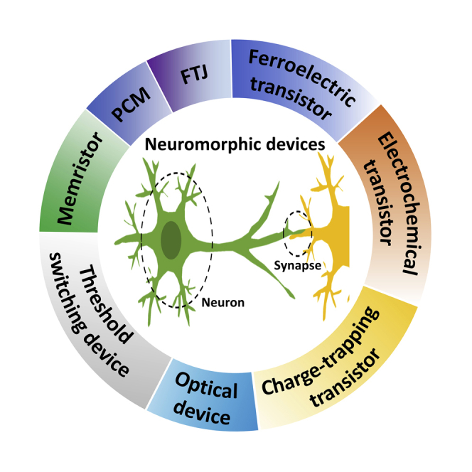
Realization of efficient neuromorphic computing systems requires development of neuromorphic devices that can emulate the functions of synapses and neurons. In neuromorphic hardware systems, neural networks can be divided into deep neural networks (DNNs) and spiking neural networks (SNNs). DNNs require artificial synapses that have analog conductance modulation characteristics because the conductance of synapses is adjusted during training by backpropagation (Burr et al., 2015; Yu, 2018). In SNNs, artificial synapses are required to emulate the spike-timing-dependent plasticity (STDP) that is used for unsupervised learning (Roy et al., 2019). Therefore, various types of memory devices have been evaluated to implement the function of synapses (Kim et al., 2018; Im et al., 2020). Artificial synapses can be categorized into two- and three-terminal devices. Two-terminal devices such as memristors, ferroelectric tunnel junctions (FTJs), and phase change memories (PCMs) have been researched as artificial synapses (Jang et al., 2019a; Li et al., 2020a; Kuzum et al., 2012a). Also, three-terminal devices including electrochemical transistors, ferroelectric transistors, and charge-trapping transistors have been researched as artificial synapses (Nikam et al., 2019; Chou et al., 2020; Kim et al., 2020a). Neural networks require emulation of the function of neurons; these functions have been achieved using memristors, PCMs, threshold switching devices, and ferroelectric transistors (Hua et al., 2019; Tuma et al., 2016; Mulaosmanovic et al., 2018a). The functions of biological synapses and neurons are successfully demonstrated in emerging memory devices, which can realize the neural networks for neuromorphic computing.
Here, we review and discuss recent development of emerging memory-based neuromorphic devices. First, we describe the functions of biological synapses and neurons, and discuss neural networks such as DNNs and SNNs. Then, we review artificial synapses for DNNs and SNNs by categorizing the types of devices into two- and three-terminal devices. Also, we introduce recent development of artificial neurons based on memristors, PCMs, threshold switching devices, and ferroelectric transistors. Finally, we present a summary and challenges for development of each device technology.
Biological Synapses and Neurons
The parallel and energy-efficient data processing capability of a brain is realized by massive interconnection of ~1011 neurons and ~1015 synapses in the neocortex, which perform memory and learning (Pakkenberg and Gundersen, 1997; Pakkenberg et al., 2003). Neurons are the basic information processing units in a biological brain, which consist of a soma (i.e., cell body), dendrites, and axons (Figure 1A). Dendrites and axons are both branched extensions of soma, but their functions are different. The dendrite receives information from the pre-synaptic neuron, and the axon transmits information to the post-synaptic neuron. The neuron can receive and transmit complex spatiotemporal information. When dendrites receive a signal from the axon terminal of the pre-synaptic neuron, the soma integrates the signal and generates action potentials (Figure 1B). The processes of signal integration and generation in biological neurons have been represented using diverse models such as integrate-and-fire, Hodgkin-Huxley, and leaky-integrate-and-fire models (Burkitt, 2006; Ma and Tang, 2017). In the leaky-integrate-and-fire model, one of the most studied neuron models, the soma generates an action potential only when the input spikes exceed a threshold value (Burkitt, 2006). The potential in the post-synaptic neuron decays over time (i.e., leaks), so to reach the threshold value, the input spikes should be nearly synchronous. After action potentials are generated, the signals are transmitted along the axon. When the signals arrive at the end of the axon, they are delivered through the synapse in the form of a chemical reaction or electrical signals, to the dendrite of the post-synaptic neuron (Pereda, 2014).
Figure 1.

Biological Neurons and Functions
(A) Schematic illustration of neuron in a biological system. Reproduced with permission (Lee et al., 2020). Copyright 2020, MDPI AG.
(B) Integrate-and-fire characteristics (bottom) in L5 pyramidal neuron as a response to fluctuating input current (top). Reproduced with permission (Pozzorini et al., 2015). Copyright 2015, Public Library of Science.
A synapse is a microscopic gap between two neurons. Neurons communicate with each other through synapses. In this process, synapses are responsible for processing and memorizing the information about signals from neurons. Synaptic transmission can entail either chemical reaction or electrical signals, so synapses can be divided into two types: chemical and electrical synapses (Pereda, 2014). Here we will only focus on chemical synapses, which are mainly found in humans. A chemical synapse has three parts: pre-synaptic terminal, post-synaptic terminal, and synaptic cleft, which is the space between pre- and post-synaptic neurons (Figure 2A). Synaptic transmission starts with the opening of calcium ion channels in the pre-synaptic neuron, which is triggered by the action potentials (Lamprecht and LeDoux, 2004). After the opening of calcium ion channels, the calcium ions diffuse into the pre-synaptic neuron and cause synaptic vesicles to release neurotransmitters. Then, neurotransmitters diffuse across the synapse and bind to receptors on the dendrite of the post-synaptic neuron; this process results in opening of sodium ion channels. The opening of the sodium ion channel causes sodium ions to diffuse into the dendrite of the post-synaptic neuron. Finally, the membrane potential of the post-synaptic neuron is changed by the amount of sodium ion uptake, and the soma generates an action potential when the membrane potential exceeds a threshold. The connection strength between two neurons is referred to as the synaptic weight and is dependent on the recent stimulation history of the synapse (Magee and Grienberger, 2020). This activity-dependent change in synaptic weight is believed to be due to synaptic plasticity, which is suggested in Hebb's postulate stating that continuous and repeated stimulation of pre-synaptic neurons can increase the synaptic weight; this process is called Hebbian learning (Caporale and Dan, 2008; Markram et al., 2011). Synaptic plasticity can be classified as short-term plasticity (STP) or long-term plasticity (LTP) according to the duration for which it is retained. In STP, synaptic weights are temporarily changed for milliseconds to a few minutes (Zucker and Regehr, 2002). The most common synaptic functions in STP are paired-pulse facilitation/depression (Atluri and Regehr, 1996). Consecutive pre-synaptic spikes can either increase or decrease the concentration of calcium ions in the pre-synaptic neuron, which results in amplified or attenuated change in post-synaptic potential or current. On the contrary, LTP is a long-term change in synaptic weight that is maintained for several hours or longer (Figure 2B) (Bliss and Lømo, 1973; Domenici et al., 1998). Due to its long-lasting properties, LTP is thought to be one of the most important functions in learning and memory (Lynch, 2004). LTP is induced by repeated and/or strong pre-synaptic spikes, which may cause changes in the size and number of the dendrites and/or receptors (Lamprecht and LeDoux, 2004). STP can be transformed to LTP by controlling the rate and/or intensity of the spikes generated from the pre-synaptic neurons (Mansuy et al., 1998; James et al., 2009).
Figure 2.

Biological Synapse and Learning Rules
(A) Schematic illustration of the synapse in a biological system. Reproduced with permission (John et al., 2018). Copyright 2018, John Wiley & Sons, Inc.
(B) Long-term potentiation characteristics (top) found in hippocampus of the anesthetized rabbit. Long-term depression (bottom) characteristics in climbing fiber synapse. Reproduced with permission (Bliss and Lømo, 1973). Copyright 1973, John Wiley & Sons, Inc. Reproduced with permission (Hansel and Linden, 2000). Copyright 2000, Elsevier Science Ltd.
(C) Types of STDP including symmetric Hebbian and anti-Hebbian; asymmetric Hebbian and anti-Hebbian learning rules. Reproduced with permission (Sharbati et al., 2018). Copyright 2018, John Wiley & Sons, Inc.
(D) STDP of biological synapse. Reproduced with permission (Bi and Poo, 1998). Copyright 1998, Society for Neuroscience.
Synaptic weight can also be changed by the temporal relationship between the pre- and post-synaptic spikes; this phenomenon is STDP (Figure 2C) (Abbott and Nelson, 2000; Citri and Malenka, 2008). Although there are numerous types of synaptic plasticity including spike-rate-dependent plasticity (SRDP) and heterosynaptic plasticity, we will focus on the STDP because it has been generally adopted in artificial neural networks. STDP can be found in various shapes and forms depending on the shape of the stimulating spike or the type of synapse (Kepecs et al., 2002; Li et al., 2014; Sharbati et al., 2018). The direction of the change in synaptic weight can be determined by the temporal order of the pre- and post-synaptic spikes. In some cases, the direction of the synaptic weight change is only determined by the relative timing of the pre- and post-synaptic spikes, and this dependency results in symmetric Hebbian or symmetric anti-Hebbian learning rule (Li et al., 2014). A biological example of the STDP with asymmetric Hebbian learning rule can be found in the hippocampus (Figure 2D) (Bi and Poo, 1998). In hippocampal neurons of rat, the synaptic weight increases when a pre-synaptic spike arrives at the synapse before the post-synaptic spike. On the contrary, the synaptic weight decreases when a post-synaptic spike arrives before the pre-synaptic spike (Bi and Poo, 1998).
Neural Network
Deep Neural Network
Neural networks consist of many neuron layers including input, hidden, and output neurons (Ielmini and Ambrogio, 2019). Each neuron is connected to all neurons in the next neuron layer by synapses (Figure 3A). In DNNs, synaptic weights of synapses (i.e., connection strength) are adjusted using backpropagation algorithms during a training process (Burr et al., 2015). DNNs have been successfully implemented using software and CMOS-based hardware, such as graphic processing units (GPUs) and CPUs. However, in these DNNs, synaptic weights are transferred between the processor and memory units, so the networks require a long time for training and consume a large amount of energy (Zidan et al., 2018; Ambrogio et al., 2018). DNNs that use artificial synapse may overcome these problems because each artificial synapse can emulate weight update characteristics of the biological synapse in a single device (Burr et al., 2015, 2017). The conductance of the artificial synapse can be used as the synaptic weight. The use of artificial synapses that have weight update characteristics can accelerate the training process and reduce power consumption (Ambrogio et al., 2018). Synaptic weight multiplies the input from pre-synaptic neuron while transferring the signal to the post-synaptic neuron (Ielmini and Ambrogio, 2019). This process enables implementation of algorithms for the summation operation (Figure 3B). During training, the synaptic weights are modified to desired values by a backpropagation algorithm. To let the synaptic weights approach the desired values as nearly as possible, artificial synapses need to have a gradual and linear synaptic weight update characteristic; linear conductance change with >100 states is required (Yu, 2018).
Figure 3.

Neural Networks
(A) Schematic illustrations of neural networks composed of input, hidden, and output neurons. Each neuron is connected by synapses to all the neurons in the next neuron layer.
(B and C) Schematic illustration of (B) DNNs and (C) SNNs. In DNNs, the inputs (x) from pre-synaptic neuron are multiplied by synaptic weights (w) and then are fed to the post-synaptic neurons. In SNNs, a neuron receives spikes from several inputs and then fires output spikes.
Spiking Neural Network
SNNs have attracted research interests for the next generation of neural networks (Maass, 1997). Compared with DNNs, the SNNs can realistically emulate the biological neural networks using biological models of the neuron to perform information coding and computation with the spatiotemporal signal processing. Neurons communicate with each other by exchanging sparse and binary spikes, and information is transferred between neurons by the frequency of spikes (Figure 3C) (Abeles et al., 1993; Hao et al., 2020). Thus, the temporal correlation between spikes in neurons is important in SNNs. These SNNs have several advantages for neuromorphic computing. The neurons in SNNs are typically silent and only active when they transmit or receive spikes (Roy et al., 2019). This computational paradigm is called event-based processing, which enables energy-efficient information processing (Roy et al., 2019). In contrast, the output layers in DNNs are sequentially processed. Each layer needs time to wait to perform the computation until the output of the previous layer is processed; this sequential process can lead to a recognition delay in the neural networks. SNNs have the advantage that they can process data in continuous time by firing spikes that show certain spatiotemporal correlations (Camuñas-Mesa et al., 2019); this is an advantage over sequential processing in DNNs.
Neurons are an important part to process the information. The neurons receive spatiotemporal signals that show the shape of the spikes from pre-synaptic neurons and transmit signals to post-synaptic neurons (Bean, 2007). The leaky-integrate-and-fire model has been applied to SNN-based neuromorphic systems because its low complexity facilitates practical application. Also, the leaky-integrate-and-fire model is considered for the neuromorphic systems because it can simultaneously emulate the integration/fire functions of spikes with spatiotemporal correlation (Yang et al., 2020). Application of SNNs for neuromorphic computing requires learning rules different from those used in DNNs. STDP has been investigated as a learning rule for the SNNs and specifically spotlighted for unsupervised training based on SNNs (Diehl and Cook, 2015). Researches to emulate STDP with various forms and to apply it to SNNs have been performed, and we will cover the contents in the section Artificial Synapses Based on Emerging Materials.
Various researches have been conducted to introduce SNNs as neural networks for neuromorphic computing, but problems remain to be solved. One main issue is the lack of efficient training algorithms and well-established datasets. For DNNs, the availability of numerous datasets has enabled training of a complex deep learning process based on backpropagation learning algorithms (Camuñas-Mesa et al., 2019). However, the training algorithms for DNNs are not directly used for SNNs (Tang et al., 2019). Spiking neurons that fire discrete spikes have discontinuous functionality that cannot be differentiable, so it is difficult to apply backpropagation algorithms based on gradient descent that is widely used for DNNs (Roy et al., 2019; Hao et al., 2020). Therefore, to properly use the SNNs for neuromorphic computing, it is essential to develop efficient learning algorithms that can consider the spatiotemporal correlations.
Artificial Synapses Based on Emerging Materials
Artificial Synapses for DNNs
Overview
Application of DNNs for high recognition accuracy requires development of artificial synapses with ideal synaptic properties (Yu, 2018). The synaptic properties of artificial synapses, such as dynamic range, multi-level states, symmetry/linearity of weight update, and retention/endurance properties can affect the accuracy of DNNs (Yu et al., 2015; Chen et al., 2017). Dynamic range is the ratio between the maximum and minimum conductance of artificial synapses. The large dynamic range is required to implement high recognition accuracy in neural networks (Yu, 2018). In DNNs, synaptic weights are adjusted during training process. For this process, an increase in the number of data states could improve learning capability and accuracy (Chen et al., 2018b). The weight update characteristics should be linear and symmetric to change the synaptic weight to the desired value during the training process (Jang et al., 2015; Jerry et al., 2018). Also, artificial synapse should have long data retention and high cycle endurance (Yu, 2018). Various types of emerging memory devices have been investigated to achieve the requirement of artificial synapses (Table 1).
Table 1.
Summary of Structures and Characteristics for Artificial Synapses
| Device Type | Structure | Operation Voltage | Operation Speed | Dynamic Range | Number of States | Power Consumption | Endurance | Ref. | |
|---|---|---|---|---|---|---|---|---|---|
| Two-terminal devices | Memristors | Ag/CιC:Ag/ITO | 1 V/−0.4 V | 20 μs/20 μs | 30 | 250 | NA | 106 | Ge et al., 2020 |
| Ag/SiGe/p-Si | 5 V/−3 V | 5 μs/5 μs | 100 | 200 | NA | 109 | Choi et al., 2018 | ||
| Phase change memory | TiN/GST/TiN | 0.9 V/4 V | 6 μs/6 μs | ∼20 | 100 | 50 pJ | 107 | Kuzum et al., 2012a | |
| Ferroelectric tunnel junctions | Pt/BTO/SNTO | 1.3 V/−1.8 V | 50 ns/50 ns | ∼12 | 200 | 0.2–146 fJ | 105 | Li et al., 2020a | |
| TiN/HfZrOx/Pt | 3 V/−3 V | 100 ns/100 ns | ∼4 | 38 | ∼1.8 pJ | 2×10² | Chen et al., 2018a | ||
| Three- terminal devices | Electrochemical transistors | Pt/Si/Li3POxSex/LiCoO3 | 1.5 V/−1.5 V | 1 s/1 s | ∼19 | 90 | NA | ∼7×10² | Nikam et al., 2019 |
| PEDOT:PPS/Nafion/PEDOT:PSS/PEI | 1.5 mV/−1.5 mV | 1 s/1 s | ∼2 | 500 | ∼10 pJ | ∼5×10³ | van de Burgt et al., 2017 | ||
| Ferroelectric transistors | IGZO/HfZrOx/TiN | 4.3 V/−3.6 V | 10 ms/10 ms | 14.4 | 64 | NA | ∼104 | Kim and Lee, 2019 | |
| Poly-GeSn/Ta2O5/HfZrOx/TiN | −8 V/8 V | 3 μs/3 μs | 9.6 | 80 | NA | NA | Chou et al., 2020 | ||
| Charge-trapping transistors | IGZO:Al NPs/Al2O3/p-Si | −4.5 V/1.5 V | 1 ms/1ms | 1.2 | 600 | NA | NA | Kim et al., 2020a | |
| CNT/SiOx/Au/SiOx/Pd | −8 V/8 V | 5 ms/100 ms | ∼50 | 120 | NA | NA | Kim et al., 2017 | ||
Two-Terminal Devices for DNNs
Two-terminal devices have a simple structure composed of active material sandwiched between two electrode layers. The conductance of the active material can be changed by applying voltage. This conductance modulation can be used to emulate the synaptic weight update characteristics. Due to simple structure and conductance modulation characteristics, various two-terminal devices such as memristors, PCMs, and FTJs have been researched as artificial synapses (Ge et al., 2020; Boybat et al., 2018; Li et al., 2020a; Chen et al., 2018a). This section reviews the device characteristics and switching mechanism of two-terminal artificial synapses for DNNs.
Memristors have been evaluated as emerging memory for artificial synapses because of their advantages such as high scalability, fast operation, and low-power consumption (Wong et al., 2012; Pan et al., 2014). The memristors are operated through conductance change, which is originated from the formation of conductive paths or modulation of oxygen vacancies distribution in the active layer by application of voltage (Pan et al., 2014). The conductance change from high-resistance state (HRS) to low-resistance state (LRS) is called a set process, whereas conductance change from LRS to HRS is called a reset process. These conductance change behaviors of memristors depend on the types of materials, operation mechanism, and device structures. A memristor composed of carboxymethyl iota-carrageenan (CιC) with Ag nanoclusters could implement synaptic weight update characteristics of DNNs (Ge et al., 2020). A CιC:Ag layer was deposited using spin-coating, and nanopores were formed in the CιC:Ag layer by adding acetic acid in the solution. In this memristor, a nanoporous CιC:Ag layer was used as a resistive switching layer. The deposition of Ag top electrode on nanoporous CιC:Ag can make a cone-shaped contact between the electrode and the switching layer, and this contact can lead to controllable and confined filament growth (Figure 4A). The memristor showed uniform resistive switching behavior with a small variation in set voltage (Figure 4B). Potentiation and depression characteristics with 250 conductance states were demonstrated by applying pulses that had increasing amplitudes (Figure 4C). The potential of a memristor based on CιC:Ag as an artificial synapse was confirmed by a simulation of neural networks. In the simulation of neural networks, recognition accuracy for Modified National Institute of Standards and Technology (MNIST) dataset was 87%. PCM is another promising candidate for artificial synapse. The PCM is composed of a phase change material sandwiched between two electrodes. Phase change materials such as Ge2Sb2Te5 (GST), GeTe/Sb2Te3, and Ag5In5Sb60Te30 have been used for PCM. The most widely researched structure of PCM has a pillar-structured heater between the phase change material and the bottom electrode, which is called a mushroom cell (or T cell). The conductance of PCM can be changed by reversible phase transformation between crystalline (high-conductance) and amorphous (low-conductance) phases (Figure 4D) (Boybat et al., 2018). For the reset process, a short current pulse with a high amplitude is applied. During this process, a significant portion of the phase change material is transformed from crystalline to amorphous phase. For the set process, a current pulse that can increase the temperature above the crystallization temperature is applied; this process induces recrystallization of the amorphous region (Wong et al., 2010). The recrystallization is affected by the amplitude and duration of the pulse, and by the number of applied pulses (Boybat et al., 2018). By progressive crystallization of amorphous region, PCM can achieve multi-level conductance characteristics. PCM that used GST as the phase change material demonstrated weight update characteristics; the device conductance of PCM increased when programming current pulses were applied (Figure 4E) (Boybat et al., 2018). The amplitude of programming pulse was varied from 50 to 120 μA. When the number of programming current pulses increased, the change in the conductance decreased and eventually saturated. Weight update characteristics of PCM were improved using voltage pulses with incremental amplitudes (Kuzum et al., 2012a). Application of voltage pulses with increasing amplitudes achieved conductance modulation through 100 steps for both potentiation and depression operations (Figure 4F). The reproducibility of this gradual conductance modulation was confirmed. FTJ can also be used as an artificial synapse. FTJ is a two-terminal device composed of a thin ferroelectric layer between two electrodes. The ferroelectric layer has polarization that can be controlled by applying an electric field and can be maintained in the absence of an electric field (Mikolajick et al., 2018). The conductance of FTJ can be modulated by the direction of polarization in a ferroelectric layer because the asymmetric screening of polarization at the interface can modulate the profile of tunnel barrier potential (Garcia and Bibes, 2014). Therefore, analog conductance switching characteristics can be achieved by controlling the polarization states to emulate synaptic weight update characteristics. FTJs composed of Pt/BaTiO3 (BTO)/Nb-doped SrTiO3 (SNTO) structure were suggested as artificial synapse (Figure 4G) (Li et al., 2020a). FTJs showed multiple conductance-voltage hysteresis loops as a function of pulse width. The conductance of the FTJs increased gradually as the pulse width increased (Figure 4H). The conductance of FTJs could be finely adjusted by controlling the amplitude and width of the pulse. These FTJs showed symmetric and linear potentiation/depression characteristics with 200 states and a dynamic range of ~12. The reproducibility of FTJ-based artificial synapses was confirmed by achieving 500 potentiation and depression cycles by applying consecutive positive and negative pulses (Figure 4I). To investigate the potential of FTJ-based artificial synapses, a simulation using potentiation and depression characteristics of FTJs was carried out. In simulation, artificial neural networks showed 96.4% recognition accuracy of the MNIST dataset.
Figure 4.

Two-Terminal Artificial Synapses for DNNs
(A) Schematic illustration of CιC:Ag-based memristor during switching.
(B) Resistive switching behaviors and set voltage variation of CιC:Ag-based memristor.
(C) Potentiation/depression characteristics of CιC:Ag-based memristor. Reproduced with permission (Ge et al., 2020). Copyright 2020, The Royal Society of Chemistry.
(D) Schematic operation mechanism of PCM. The crystalline region can be gradually increased by application of potentiation pulses.
(E) The potentiation characteristics of PCM based on GST with different programming current amplitudes (Iprog). Reproduced with permission (Boybat et al., 2018). Copyright 2018, Springer Nature.
(F) Gradual reset and set characteristic of PCM based on GST. Gradual reset is performed by using pulses with incremental amplitude from 2 to 4 V (20-mV voltage steps). Gradual set is performed by using staircase pulse scheme including 20 pulses for each voltage step (0.5, 0.6, 0.7, 0.8, and 0.9 V). Reproduced with permission (Kuzum et al., 2012a). Copyright 2012, American Chemical Society.
(G) Schematic illustration of an FTJ-based artificial synapse with Pt/BaTiO3 (BTO)/Nb-doped SrTiO3 (SNTO) structure.
(H) Multiple conductance-voltage (G-V) hysteresis loop as a function of pulse width.
(I) Potentiation and depression characteristics with 200 states for 500 cycles. Positive voltage (1.3 V, 50 ns) and negative voltage pulses (−1.75, 50 ns) pulses were used for potentiation and depression operation, respectively. Reproduced with permission (Li et al., 2020a). Copyright 2020, John Wiley & Sons, Inc.
Three-Terminal Devices for DNNs
Artificial synapses with a three-terminal structure have an additional terminal to control the synaptic weights. The additional terminal can complicate the device structure, but can also improve the controllability of synaptic characteristics and prevent sneak paths in the array (Kim et al., 2020b). Therefore, three-terminal devices including electrochemical, ferroelectric, and charge-trapping transistors have been evaluated as artificial synapse for DNNs (van de Burgt et al., 2017; Fuller et al., 2017; Jerry et al., 2018; Kim and Lee, 2019; Kim et al., 2017; Yi et al., 2018). This section reviews three-terminal artificial synapses for DNNs.
Electrochemical transistors showed linear and symmetric conductance modulation characteristics, so they have been considered as promising candidates for artificial synapses. The devices are composed of an electrolyte, a channel, and gate/source/drain electrodes. The channel conductance of electrochemical transistors can be controlled by applying electrical pulses to the gate electrode (van de Burgt et al., 2018). The pulses drive mobile ions such as Li+, H+, and O2− in an electrolyte into or out of the channel. The injected or extracted mobile ions can change the doping level of the channel layer, and this change induces a change in channel conductance. This characteristic can be used to achieve multi-level conductance, which is required for emulation of potentiation and depression characteristics. However, electrochemical transistors have suffered from small dynamic range and short retention issues. An electrochemical transistor composed of a Se-doped lithium phosphate (Li3POxSex) electrolyte with a high ionic conductivity was proposed as an artificial synapse (Figure 5A) (Nikam et al., 2019). For comparison, an electrochemical transistor was also fabricated using lithium phosphate (Li3PO4) as an electrolyte that had lower ionic conductivity compared with Li3POxSex. When negative voltage pulses were applied to Li3PO4-based electrochemical transistor, the channel conductance gradually increased. However, the conductance change after application of voltage was unstable and volatile (Figure 5B). In contrast, the conductance change of Li3POxSex-based electrochemical transistor was stable and nonvolatile (Figure 5C). The nonvolatility in Li3POxSex-based electrochemical transistor originated from the fast ionic conduction through the electrolyte layer. This Li3POxSex-based electrochemical transistor showed symmetric and linear potentiation/depression characteristics with 90 states and dynamic range of ~19 (Figure 5D). To confirm the applicability of these Li3POxSex-based electrochemical transistors as artificial synapses, a simulation was carried out. In simulated artificial neural networks, 91% recognition accuracy of the MNIST dataset was achieved. Ferroelectric transistors have also been considered as artificial synapses (Oh et al., 2019). A ferroelectric transistor is a kind of transistor that uses ferroelectric material as a gate dielectric layer. The ferroelectric layer controls the carrier concentration at the surface of a channel layer, so the channel conductance of a ferroelectric transistor can be adjusted by modulating the polarization states of ferroelectric layer (Kaneko et al., 2011). The polarization states can be modulated by controlling the amplitude and width of the applied pulses (Alessandri et al., 2018). The weight update characteristics can be achieved by adjusting the state of polarization in a ferroelectric layer. There have been attempts to use the ferroelectric transistor as artificial synapses. However, the development of artificial synapses based on ferroelectric transistors has been limited due to the disadvantages of traditional ferroelectric materials such as high annealing temperatures, complex compositions, and difficulty in scaling (Horiuchi et al., 2009; Mikolajick et al., 2018). Hafnia-based ferroelectric materials can be used to overcome the disadvantages of traditional ferroelectric materials due to their advantages such as low annealing temperatures, CMOS compatibility, and scalability (Kim et al., 2019b). Ferroelectric transistors with hafnia-based ferroelectric materials have the potential to be used for artificial synapses. One ferroelectric transistor composed of a zirconium-doped hafnium oxide (HfZrOx) and an indium gallium zinc oxide (IGZO) was suggested as an artificial synapse (Kim and Lee, 2019). HfZrOx and IGZO were used as ferroelectric and channel layers, respectively. The conductance of the IGZO channel depended on the polarization states of HfZrOx. The transistor showed linear weight update characteristics with 64 states and dynamic range of 14.4. A HfZrOx-based ferroelectric transistor with a poly-GeSn channel was also proposed as a synaptic transistor (Figure 5E) (Chou et al., 2020). In this device, NH3 plasma treatment of poly-GeSn and the interfacial layer was used to improve the endurance and retention characteristics. This ferroelectric transistor showed linear and symmetric weight update characteristics with 80 states and dynamic range of 9.6 (Figures 5F and 5G). The applicability of HfZrOx-based ferroelectric transistors as artificial synapses was verified by a simulation that achieved 91.4% recognition accuracy of the MNIST dataset. Charge-trapping transistors have been investigated as artificial synapses for DNNs. Charge-trapping transistors have trapping sites such as nanoparticles (NPs) that can trap electrons or holes. When an electrical field is applied, the carriers can be trapped in the trapping sites, which lead to change of the device conductance. By controlling the number of trapped charge carriers, analog memory characteristics can be achieved. A charge-trapping transistor composed of IGZO with Al NPs was suggested as artificial synapse (Figure 5H) (Kim et al., 2020a). Al NPs were used for charge-trapping sites to control the conductance of the devices. When positive voltage was applied to the gate electrode, electrons at the surface of IGZO layer were trapped at the shallow energy states on Al NPs, so the conductance of the IGZO channel decreased. Under negative gate voltage, the trapped electrons were released to the IGZO layer, so its conductance increased (Figure 5I). Potentiation and depression characteristics were achieved by applying negative and positive pulses, respectively (Figure 5J). To confirm the feasibility of these charge-trapping transistors as artificial synapses for neuromorphic computing, artificial neural networks were simulated. In the simulation, the recognition accuracy of the MNIST dataset was 90.1%.
Figure 5.

Three-Terminal Artificial Synapses for DNNs
(A) Schematic illustration of electrochemical transistor with a Li3POxSex electrolyte.
(B and C) Conductance modulation characteristics of electrochemical transistor based on (B) Li3PO4 and (C) Li3POxSex.
(D) Potentiation/depression of Li3POxSex-based electrochemical transistor using 90 identical pulses (±1.5 V, 1 s). Reproduced with permission (Nikam et al., 2019). Copyright 2019, Springer Nature.
(E) Schematic illustration of ferroelectric transistor composed of HfZrOx and poly-GeSn.
(F and G) (F) Potentiation and (G) depression characteristics of devices using HfZrOx. Reproduced with permission (Chou et al., 2020). Copyright 2020, American Chemical Society.
(H) Schematic illustration of charge-trapping transistor with IGZO:Al NPs/Al2O3/p+ Si structure.
(I) Schematic operation mechanism of charge-trapping transistor.
(J) Potentiation/depression of charge-trapping transistor. Reproduced with permission (Kim et al., 2020a). Copyright 2020, John Wiley & Sons, Inc.
Artificial Synapses for SNNs
Overview
Although DNNs show its plausibility for energy-efficient and error-tolerant computation by mimicking the fundamental data processing structure of the biological brain, they usually require real-valued signals and non-biological learning algorithms such as back-propagation (LeCun et al., 2015; Wang et al., 2018a). Thus, complex information with spatiotemporal characteristics is hard to be processed with DNNs (LeCun et al., 2015). SNNs have been developed to process complex information by emulating the form of the signals (i.e., binary spikes) and learning algorithms (i.e., STDP) of the brain (Ponulak and Kasinski, 2011). For the development of SNNs, diverse types of artificial synapses that have STDP characteristics have been evaluated (Wang et al., 2019; Ielmini and Ambrogio, 2019). In this section, we will focus on the characteristics and operation mechanism of artificial synapses for SNNs.
Two-Terminal Devices for SNNs
Learning and memorization in a brain usually occur by an unsupervised process, such as STDP (Debanne et al., 1998). In these learning rules, the timing of the spikes between two neurons can lead to potentiation or depression of the synapses (Debanne et al., 1998; Zhang et al., 1998). As the spatiotemporal variables such as time and space are essential for computing information in SNNs, there have been several attempts to implement STDP in artificial synapses (Ponulak and Kasinski, 2011). In this section, we will focus on the device characteristics and working mechanism of the two-terminal artificial synapses for SNNs.
In memristor devices, two approaches are usually used to implement STDP characteristics. The first approach is to use a CMOS circuit as a neuron, and one-resistor (1R) as an artificial synapse (Figure 6A) (Jo et al., 2010). In this approach, artificial synapses undergo resistance change by voltage pulses generated by artificial neurons, which can convert incoming information to voltage pulses. The relative timing between pre- and post-neuron spikes leads to a change in the synaptic weight of the artificial synapse. For example, when the spike from the pre-synaptic neuron arrives before the spike from the post-synaptic neuron, the synaptic weight of the artificial synapse increases (i.e., potentiation). With different spike timing, the 1R synapse shows asymmetric anti-Hebbian learning rule, which can also be found in biological components such as hippocampal neurons (Figure 6B). SNNs that use this structure can recognize binary patterns. However, although SNNs that use the artificial synapse with 1R structure have the advantages of simple structure and high density, the use of this structure for complex tasks is impeded by disadvantages such as abrupt switching of the memristor, sneak current paths, and disturbance from adjacent cells.
Figure 6.

Two-Terminal Artificial Synapses for SNN
(A) Schematic illustration of neural network composed of CMOS neurons and memristor synapses.
(B) STDP characteristics obtained using a memristor synapse (left) and a hippocampal neuron of a rat (right). Insets: scanning-electron microscope image of a memristor crossbar array. Scale bar: 300 nm (left). A phase contrast image of a hippocampal neuron. Scale bar: 50 μm (right). Reproduced with permission (Jo et al., 2010). Copyright 2010, American Chemical Society.
(C) Schematic illustration of 1T1R synapse. The pre-synaptic neuron (PRE) and the post-synaptic neuron (POST) are connected to gate electrode and the source of the transistor, respectively. The POST is also connected to the resistor to apply feedback spike to the 1T1R synapse.
(D) Synaptic weight change after PRE (Vaxon) and POST (VTE) spikes. Short (left) and long (right) delays (Δt = tPRE-tPOST) lead to strong and weak potentiation, respectively.
(E) Relative synaptic weight change (G/G0) depending on Δt. Reproduced with permission (Wang et al., 2018a). Copyright 2018, American Association for Advancement of Science.
(F) Resistance hysteresis loops of synaptic FTJs depending on voltage pulse amplitudes.
(G and H) STDP learning rules with (G) asymmetric and (H) symmetric forms obtained using FTJs. Reproduced with permission (Majumdar et al., 2019). Copyright 2019, John Wiley & Sons, Inc.
Artificial synapse with one-transistor/one-resistor (1T1R) structure may overcome the above problems in SNNs (Wang et al., 2018a, Wang et al., 2019). The 1T1R synapse was constructed by connecting the resistor to the drain electrode of the transistor. In 1T1R structure, the transistor inside the synapse reduced the leakage current from sneak paths and disturbance from adjacent cells and increased the switching uniformity of the memristor device (Figure 6C) (Wang et al., 2018a). To implement 1T1R synapse, the pre-synaptic CMOS neuron was connected to the gate electrode of the transistor and the post-synaptic CMOS neuron was connected to both source electrode of the transistor and the resistor, to apply a feedback spike to the 1T1R synapse. The synaptic weight of 1T1R synapses was updated by the Widrow-Hoff learning rule, in which the post-synaptic CMOS neuron compared the output signal and teacher signal to identify whether the spike pattern was true or false. This learning rule was realized in the 1T1R synapse by potentiating the resistor using a positive voltage spike (VTE+) when only the teacher signal was present and by depressing the resistor using a negative voltage spike (VTE-) when only signals from the post-synaptic CMOS neuron were present. The time delay between spikes from pre- and post-synaptic CMOS neurons showed a strong relationship with the change of synaptic weight, which corresponds to STDP characteristics (Figures 6D and 6E). Other types of artificial synapses such as FTJs and PCMs have also been suggested for use in SNNs (Boyn et al., 2017; Majumdar et al., 2019; Kuzum et al., 2012b). Artificial synapse based on FTJ has been demonstrated using SNTO, poly(vinylidene fluoride/trifluoroethylene) [P(VDF-TrFE)], and Au as a substrate, ferroelectric tunnel barrier, and top electrode, respectively (Majumdar et al., 2019). In FTJs, the application of voltage pulses can modify the ferroelectric domain population, which induces the change in tunneling resistance. The change of polarization state was affected by the amplitude and length of voltage pulses, so the resistance state of the FTJs could also be controlled by voltage pulses (Figure 6F). Asymmetric and symmetric STDP learning rules were realized by applying different voltage waveforms (Figures 6G and 6H). Similar STDP learning rules were also demonstrated in FTJs using Co, BiFeO3, and Ca0.96Ce0.04MnO3 as a top electrode, ferroelectric tunnel barrier, and bottom electrode, respectively (Boyn et al., 2017). Artificial synapses based on PCM have also shown their plausibility for use in SNNs (Kuzum et al., 2012a, 2012b). PCM was introduced using GST that could be switched reversibly between amorphous and crystalline phases by application of external voltage. The devices were fabricated as a mushroom-like two-terminal device with a pillar-shaped heating material positioned between the chalcogenide material and the bottom electrode. By controlling the amplitude and length of the voltage pulse, analog switching characteristics were achieved due to the gradual increase of amorphous or crystalline regions of chalcogenide material. Symmetric and asymmetric STDP characteristics were achieved by applying two voltage pulses (i.e., pre- and post-synaptic spikes) with a controlled timing difference. Furthermore, the time constant of the STDP learning rule can be tuned by modulating the amplitude and length of the voltage pulse (Chen et al., 2013).
Although the aforementioned reports show successful implementation of STDP learning rules in artificial synapses, other bio-plausible learning rules are also being demonstrated in artificial synapses for realization of bio-realistic neural networks. In biological neurons, the change of synaptic weight is dependent not only on the condition of stimuli but also on the recent activation history (Abraham, 2008). Thus, the results (i.e., change of synaptic weight) in response to stimuli can be different although the condition of stimulation is the same; this phenomenon is referred as metaplasticity (Abraham, 2008). To emulate metaplasticity in artificial synapses, the conditions of stimulus such as current compliance and spike interval were modulated (Tan et al., 2016; Liu et al., 2018). Artificial synapse based on Pt/WO3/Pt structure demonstrated that the STDP learning rules can be affected by previous activation history (i.e., metaplasticity) when the device was stimulated by designed voltage pulses separated with different pulse intervals (Tan et al., 2016). In these devices, the working mechanism may be the migration and spontaneous diffusion of activated oxygen vacancies driven by the electric field. Metaplasticity has also been demonstrated using artificial synapse with Al/AlOx/graphene structure (Liu et al., 2018). The post-synaptic current of the device showed activity-dependent metaplasticity using prior set process with different current compliance. The programmable metaplasticity was also demonstrated by precisely controlling the filament size using current compliance.
Three-Terminal Devices for SNNs
The introduction of an additional electrode can be advantageous for precise control of the device conductance compared with two-terminal devices. The three-terminal devices can simultaneously perform learning functions and signal transmission because signals are transmitted to the channel, whereas the synaptic manipulation can be performed by the gate electrode (Balakrishna Pillai and De Souza, 2017; Yang et al., 2017). Due to these advantages, three-terminal devices have been applied as artificial synapses. In this section, artificial synapses that use three-terminal devices for SNNs are reviewed.
Organic electrochemical transistors (OECTs) have been investigated for neuromorphic applications (Gkoupidenis et al., 2015; van de Burgt et al., 2017; Fu et al., 2018). An OECT is composed of an organic semiconductor and an electrolyte with the gate, source, and drain electrodes (Rivnay et al., 2018). The OECT operates when ions are injected from the electrolyte into the organic semiconductor; as a result its doping state changes, so its conductivity changes (Bernards and Malliaras, 2007; Rivnay et al., 2018). An artificial synapse based on OECT has been proposed (Fu et al., 2018). An artificial synapse was composed of poly(3-hexylthiophene) (P3HT) channel and ion-gel that was used as a gate electrolyte and a substrate (Figure 7A). Electrochemical doping of ions between P3HT and ion-gel by gate voltage yielded nonvolatile synaptic behaviors. When pulses were applied to the gate electrode as pre-synaptic spikes and to the drain electrode as post-synaptic spikes, artificial synapses showed various STDP (asymmetric and symmetric Hebbian learning; asymmetric and symmetric anti-Hebbian) functions that occur in a biological synapse. For asymmetric STDP functions (Figure 7B), a post-synaptic spike composed of two right-angled triangular pulses and a rectangular pre-synaptic spike were used (Figure 7C). By controlling the time interval between successive spikes, asymmetric STDP characteristic was realized. The charge-trapping and charge-detrapping effects in transistors have been exploited for artificial synapses. An artificial synapse based on the charge-trapping effect was fabricated using a semiconducting-enriched single-walled carbon nanotube (CNT) matrix (Figure 7D) (Kim et al., 2015). In the transistor device, the gate and source electrodes were connected to pre- and post-synaptic neurons, respectively. The variable channel conductance based on hysteresis in the CNT transistor was used as a synaptic weight. The hysteresis occurred due to charge-trapping and charge-detrapping effects, which led to analog channel conductance switching behaviors. These behaviors enabled implementation of synaptic functions. STDP characteristics were realized by applying pre- and post-spikes that were separated by different time intervals (Figure 7E). Additionally, a system-level simulation of pattern recognition by an SNN that used synaptic transistors associated with CMOS neurons and a simplified STDP scheme showed an average recognition accuracy of 60% for unsupervised learning (Figure 7F). The ferroelectric transistor is one of the promising candidates for an artificial synapse to implement STDP (Mulaosmanovic et al., 2017; Jang et al., 2019b; Zhou et al., 2019). By adjusting the polarization states of the layer by an electric field, the device can achieve analog switching characteristics to emulate synaptic plasticity. A synaptic transistor based on ferroelectric copolymer P(VDF-TrFE) was proposed. P(VDF-TrFE) copolymer and pentacene were used as the ferroelectric layer and the channel layer, respectively (Figure 7G) (Jang et al., 2019b). Hysteresis behavior was observed in the current-voltage curve when the gate voltage was swept between ±30 V. This behavior was induced by polarization switching of the ferroelectric domain in P(VDF-TrFE) copolymer (Figure 7H). Synaptic functions could be emulated by adjusting the polarization state. Asymmetric STDP characteristic was implemented by applying pulse trains to the gate and drain electrodes (Figure 7I). STDP characteristics were controlled by modulating the time interval between successive spikes.
Figure 7.

Three-Terminal Devices for SNN
(A) Schematic structure of the device composed of P3HT and ion-gel.
(B) Asymmetric STDP characteristics of P3HT-based artificial synapse.
(C) Waveforms of pre- and post-spikes to achieve STDP. Reproduced with permission (Fu et al., 2018). Copyright 2018, American Chemical Society.
(D) Schematic illustration of carbon nanotube (CNT) synaptic transistor and atomic force microscopic images of single-walled CNT.
(E) STDP function in the device CNT-based artificial synapse.
(F) The architecture of artificial neural networks using CNT synaptic transistor. Reproduced with permission (Kim et al., 2015). Copyright 2015, American Chemical Society.
(G) Schematic structure of the device composed of P(VDF-TrFE) and pentacene.
(H) Transfer characteristics of the ferroelectric organic neuromorphic transistor.
(I) Implementation of the asymmetric STDP functions using organic-based artificial synapse. Reproduced with permission (Jang et al., 2019b). Copyright 2019, American Chemical Society.
Similar to two-terminal artificial synapses for SNNs, there have been diverse efforts to emulate bio-plausible learning rules in three-terminal artificial synapses (Gkoupidenis et al., 2017; Ren et al., 2019). A synaptic transistor using indium tin oxide (ITO) channel and chitosan electrolyte was proposed to emulate activity-dependent metaplasticity (Ren et al., 2019). In the device, it was demonstrated that excitatory post-synaptic current characteristics can be controlled by applying priming voltage spikes. By controlling the condition of priming voltage spikes, metaplastic facilitation and inhibition of LTP were demonstrated. This activity-dependent metaplasticity was realized by proton accumulation due to electric field and spontaneous diffusion. In OECTs, the demonstration of global gating enabled global modulation of synaptic weights; this response is similar to homeostatic plasticity in a biological brain (Gkoupidenis et al., 2017). Homeostatic plasticity is one of the bio-plausible learning rules that can stabilize the activity of the neuron from its positive feedback loop (Turrigiano and Nelson, 2004). With a 4 × 4 array of PEDOT:PSS-based OECTs and a global NaCl electrolyte, the response of the OECTs in the array can be controlled globally. Also, the OECTs in the array can communicate through the global electrolyte. Dendritic functions of neural networks have been emulated using an ionic-gated field-effect transistor with a multi-terminal structure (Li et al., 2020c). The device was composed of two ionic gate terminals and silicon nanowire channel, which acted as pre-synapses and a dendrite that could integrate signals, respectively. When spikes with different frequencies were applied to each ionic gate terminal, the spikes were integrated in the silicon nanowire channel layer, and different current change was observed depending on the degree of the integration. These behaviors enabled the realization of the dendritic integration and computation such as “Add” and “Subtract.”
Artificial Neurons Based on Emerging Materials
Overview
In a biological system, neural networks are composed of neurons connected by synapses. A biological neuron receives the input signals from pre-synaptic neurons through the connecting synapses and generates an action potential to the post-synaptic neurons when membrane potential exceeds a threshold level (Figure 8A) (Bean, 2007). To achieve brain-inspired neuromorphic computing in hardware, biological neural networks should be mimicked using electronic devices. The integrate-and-fire neuron is widely used to emulate biological neural networks due to its low complexity. This neuron integrates input currents through synapses and fires spikes to the next synapse layer if the integrated potential exceeds the threshold voltage (Figure 8B). Implementation of efficient neural networks requires development of neurons that can receive and fire the signals. Integrate-and-fire neuron circuits that use CMOS technology generally require tens of transistors, which lead to a large device area and high power consumption (Kadetotad et al., 2015; Gao et al., 2017). To overcome these problems, emerging devices such as memristors, PCM, and ferroelectric devices have been evaluated for use as artificial neurons. In this section, various emerging devices-based artificial neurons are reviewed.
Figure 8.

Artificial Neurons Based on Memristors
(A) Schematic illustration of biological neurons and synapse. Signals are transferred from pre-to post-synaptic neuron through a synapse.
(B) Equivalent electronic systems to a biological synapse. Neurons accumulate inputs generated by different pre-synaptic neurons and fire spikes to the next synapse. Reproduced with permission (Hua et al., 2019). Copyright 2019, John Wiley & Sons, Inc.
(C) Operation principle of threshold switching-based artificial neuron.
(D) Integrate-and-fire behavior of an artificial neuron based on B0.25Te0.75 (B-Te) at different current amplitudes. Reproduced with permission (Lee et al., 2019). Copyright 2019, John Wiley & Sons, Inc.
(E) Oscillation of voltage across the diffusive memristor under application of voltage pulse (1 V).
(F) A magnified view of the oscillation.
(G) The oscillation frequency of neuron depending on the resistance of a load memristor. Reproduced with permission (Midya et al., 2019). Copyright 2019, John Wiley & Sons, Inc.
Artificial Neuron Based on Memristor
Memristors can implement the integrate-and-fire functions of biological neurons (Mehonic and Kenyon, 2016; Lashkare et al., 2018). An artificial neuron based on Pr0.7Ca0.3MnO3 (PCMO) showed resistive switching behavior by the transport of oxygen ions in PCMO (Lashkare et al., 2018). To implement integrate-and-fire functions, short voltage pulses (200 ns) that caused a slow current change were applied instead of long pulses (1 μs) to avoid abrupt current change. First, the conductance changed slowly during application of consecutive short pulses (integration); when conductance reached a critical level, the conductance could rapidly increase in a single pulse, i.e., the firing of the neuron. After the firing process, a reset pulse was applied, and the conductance of device was recovered to the state that it was in before the integration process. Repetition of these processes achieved sequential integrate-and-fire functions. Volatile threshold switching devices have been evaluated for artificial neurons (Gao et al., 2017; Wang et al., 2018b; Chatterjee and Kottantharayil, 2019). The volatile threshold switching devices have a two-terminal structure composed of an active layer between two electrodes, which is similar to the structure of a memristor. However, these devices only show a temporary change in resistance. The volatile threshold switching device is operated by change of resistance from HRS to LRS when a voltage higher than the threshold voltage is applied and from LRS to HRS after removal of the applied voltage. Such threshold switching devices do not require additional circuits to reset the device resistance to the initial state, so they can be used to reduce the device area and power consumption. An integrate-and-fire neuron circuit based on a threshold switching device is composed of a threshold switching device and a capacitor (Figure 8C). First, the integration process is performed in this circuit; when input pulses are applied, the capacitor begins to be charged. The total charge in the capacitor increases when the pulses are continuously applied; this process leads to increase in the voltage drop of the threshold switching device in the circuit. When the voltage drop of the threshold switching device reaches a threshold voltage, the device is turned on and fires the output spikes. After the firing process, the capacitor is discharged through a threshold switching device that is turned on; this result leads to a decrease of the voltage drop in the device, so it is turned off and returns to the state that it was in before the integration process. Repetition of these processes yields consecutive integrate-and-fire functions. Various threshold switching devices including insulator-to-metal transition-based device using NbO2, ovonic threshold switch based on B0.25Te0.75 (B-Te), and atomic switch device using Ag/HfO2 structure were evaluated for integrate-and-fire neurons (Lee et al., 2019). In all cases, the behaviors of integrate-and-fire were observed. The artificial neuron that used B-Te showed fast switching speed and slow discharging process in the interval between pulses (Figure 8D). The slow discharging process was induced by a high off-state resistance (Roff) of B-Te-based device. In addition, the possibility of implementation of leaky characteristics was investigated using the three threshold switching devices. The amount of discharge in the interval between pulses was considered as a leaky characteristic; a small amount of discharge was regarded as a nonleaky characteristic. The artificial neuron based on NbO2 showed fast discharge (i.e., was leaky), whereas the artificial neuron based on B-Te and Ag/HfO2 showed slow discharge (i.e., was not leaky). It indicated that NbO2-based neuron could achieve leaky characteristic, whereas nonleaky characteristic was implemented by B-Te- and Ag/HfO2-based artificial neurons. Also, the simulation was performed to confirm the applicability of the integrate-and-fire neurons in neural networks. Two-layer perceptron neural networks were used for the recognition of handwritten digits. When digit “2” was applied to the input, a large number of spikes were released from the output neuron that matched digit “2” compared with other output neurons. A diffusive memristor with Pt/SiOxNy:Ag/Pt structure was evaluated as an artificial neuron. To demonstrate the oscillation neuron function, a relaxation oscillator was constructed using a diffusive memristor connected to capacitor and a load memristor that had Pd/HfO2/Ta structure. The voltage across the diffusive memristor oscillated when a voltage of 1 V was applied (Figures 8E and 8F). The frequency of the oscillation was controlled by the resistance of the memristor and the capacitance of the connected capacitor. When the resistance of a load memristor was low, the RC constant became small, so the oscillation had high frequency (Figure 8G). The properties of an artificial neuron based on diffusive memristor were evaluated in an array composed of 32 synapses and one neuron. The synaptic weight-voltage products were summed at the end of the column and translated to time-varying current. Also, synaptic weight was controlled depending on input voltage, which led to oscillation behaviors with different frequencies (Midya et al., 2019).
Furthermore, several efforts have been made to implement other essential components of biological neural networks. Dendrites are one of the important building blocks for information processing in a biological neural network (Takahashi et al., 2016). They perform the nonlinear integration of synaptic signals and filter out irrelevant background information; this selectivity is one of the reasons why complex information can be processed with low power consumption in biological neural networks (Li et al., 2020b). To emulate the function of dendrite, an artificial dendrite has been developed using a memristor with Pt/TaOx/AlOx/Al structure. The device was operated by formation and migration of oxygen interstitials in the TaOx layer. AlOx was used as the reservoir layer that could accept the oxygen interstitials. In the off-state, the device filtered small input signals, but in the on-state it achieved nonlinear integration of input signals. Furthermore, the artificial dendrite was applied to a complete neural network that included artificial synapses and a soma. The neural network consumed less power than a combination of CPU and application-specific integrated circuit.
Artificial Neuron Based on Ferroelectric Device
Ferroelectric materials have been evaluated as components for neuromorphic computing (Mulaosmanovic et al., 2018a; Dutta et al., 2019; Chen et al., 2019). The polarization state of the ferroelectric material can be tuned reversibly by controlling an applied electric field. Accumulative switching behavior in the ferroelectric transistors makes them suitable as artificial neurons (Mulaosmanovic et al., 2018b). An artificial neuron based on a ferroelectric transistor had a TiN/Si:HfO2/SiON/Si structure (Figure 9A) (Mulaosmanovic et al., 2018a). Si:HfO2 and SiON were used as a ferroelectric layer and a dielectric (interface) layer, respectively. Integrate-and-fire behavior in the ferroelectric transistor was induced by application of a pulse shorter than the switching threshold (Figure 9B). The state of the device was not changed by a short pulse, but when these short pulses were applied consecutively, a cumulative effect was induced within the ferroelectric material. After application of 21 pulses, the ferroelectric transistor switched abruptly from the off- to the on-state. The change occurred by application of pulses that caused nucleation of nanodomains in the ferroelectric layer. When a small number of pulses was applied, the number of nanodomains was insufficient to induce a charge inversion, so the off-state was maintained. However, when sufficient number of pulses were applied, a critical number of nanodomains nucleated, which led to the abrupt polarization reversal. This polarization reversal induced a charge inversion in the channel, so the state changed from the off- to on-state. The characteristics of integrate-and-fire functions were achieved in these neurons by adjusting the amplitude of the applied voltage pulses (Figure 9C). Also, an attempt was made to implement leaky characteristics using ferroelectric transistor by applying negative bias during the time interval between successive positive input pulses; the negative bias inhibited the creation of ferroelectric domains. The behavior was controlled by the amplitude of applied negative bias. Application of a high-amplitude negative bias increased the number of positive pulses required to induce switching behavior.
Figure 9.

Artificial Neurons Based on Ferroelectric Transistor
(A) Schematic illustration of ferroelectric transistor based on TiN/Si:HfO2/SiON/Si.
(B) Implementation of integrate-and-fire functions using a ferroelectric transistor.
(C) Consecutive integrate-and-fire behaviors with different voltage amplitudes. Reproduced with permission (Mulaosmanovic et al., 2018a). Copyright 2018, The Royal Society of Chemistry.
Artificial Neuron Based on Phase Change Memory
Although gradual modulation of device conductance has been utilized in PCM-based artificial synapses, PCM-based artificial neuron requires firing characteristics after they are stimulated by a certain number of voltage pulses; this is a different response than the gradual modulation of device conductance in artificial synapses that use PCM (Kuzum et al., 2012a; Ielmini and Ambrogio, 2019). Also, nonvolatile memory characteristics are not mandatory for artificial neurons, because they can use volatile switching characteristics to implement the integrate-and-fire function of the biological neuron (Wang et al., 2017a). In phase change neurons, the effective thickness of the amorphous (i.e., high-resistance) region of chalcogenide material can be considered equivalent to the membrane potential of a biological neuron (Pantazi et al., 2016; Tuma et al., 2016). Theoretical and experimental results indicate that the growth of amorphous region in chalcogenide material can be precisely designed by controlling the voltage pulse condition (Sebastian et al., 2014; Tuma et al., 2016). The application of multiple designed-voltage pulses can induce a controlled crystallization that can lead to a sudden change in the device conductance, which resembles the integrate-and-fire characteristics of the biological neuron. After firing, reset process was done using a voltage pulse. The amplitude of the voltage pulse is one of the most important parameters for controlled crystallization, so the firing rate of PCM-based artificial neurons can be manipulated by controlling the amplitude of voltage pulses. Also, detection of temporal correlations of data streams was demonstrated using the neuromorphic circuit composed of PCM-based artificial neurons and PCM-based artificial synapses (Pantazi et al., 2016). PCM-based artificial neurons were also demonstrated in 1T1R structure (Pedretti et al., 2020). 1T1R-structured artificial neuron also showed integrate-and-fire characteristics under consecutive voltage pulses (Figure 10A). The number of voltage pulses required for a sharp increase in device conductance (i.e., firing) varied, possibly because of stochastic nucleation and growth of the amorphous region in chalcogenide material (Russo et al., 2006; Tuma et al., 2016). As the amplitude of the voltage pulse can affect the crystalline state of a chalcogenide material, the required number of voltage pulses to induce firing can be manipulated by controlling the amplitude of set voltage (Vset) and that of reset voltage (Vreset) (Figure 10B). For example, the number of voltage pulses required for firing increased with increasing Vreset, as higher Vreset results in larger amorphous volume. The firing rate of 1T1R-structured artificial neurons can also be manipulated by controlling the amplitude of voltage pulses; this response is similar to 1R-structured artificial neurons that use PCM (Figure 10C).
Figure 10.

Artificial Neurons Based on Phase Change Materials and Photonic Application
(A) Relative change in conductance (G/G0) depending on the number of pulses (Nc).
(B) Average Nc to reach a threshold conductance (Gth = Gsat/2) depending on pulse amplitude for set process (Vset) and reset process (Vreset).
(C) Integrate-and-fire characteristics in a phase change neuron. The firing frequency of the artificial neuron can be controlled by the amplitude of the applied voltage pulse. Reproduced with permission (Pedretti et al., 2020). Copyright 2020, Pedretti et al.
(D) Schematic illustration of the ring resonator with GST. The transmission of light through DROP and THROUGH port can be controlled by crystalline state of GST.
(E) Schematic illustration of photonic neuron based on GST-embedded ring resonator.
(F) Change of membrane potential in photonic neuron after write and reset pulses. Reproduced with permission (Chakraborty et al., 2018). Copyright 2018, Springer Nature.
(G) I-V characteristics under dark and UV illumination in memristor based on InP/ZnS core-shell QDs.
(H) Schematic illustrations of biological neuron and neuromorphic circuit using the InP/ZnS-based memristor.
(I) Integration-and-fire behavior emulated by InP/ZnS-based memristor. Reproduced with permission (Wang et al., 2020). Copyright 2020, John Wiley & Sons, Inc.
Artificial Neuron Based on Photonic Devices
Optical or electrical stimuli can switch the crystallinity of the material such as GST between the amorphous state that has low optical reflectivity and the crystalline state that has high optical reflectivity. To exploit this light-responsive characteristic of GST, a photonic neuron based on a ring resonator structure was suggested (Figure 10D) (Chakraborty et al., 2018, 2019). The ring resonator was a set of two rectangular optical waveguides and a ring optical waveguide. In ring resonators, the direction of the wave that enters the "INPUT” port could be guided to the "THROUGH” port or "DROP” port by controlling the coupling (t1, t2) and attenuation parameters (k1, k2). With a GST layer on the ring waveguide, the attenuation parameters could be controlled by the crystalline state of the GST. When the GST was in crystalline and amorphous state, the direction of the wave entering the “INPUT” was guided to the "THROUGH” and "DROP,” respectively. The GST-based optical neuron was constructed with two components, which are the integration unit and the firing unit (Figure 10E). The integration unit consisted of two GST-embedded ring resonators; the firing unit consisted of a photonic amplifier, a circulator, and a GST-embedded rectangular waveguide. For the integration unit, two GST-embedded ring resonators were used to separately perform integration of positive signals with one ring resonator and integration of negative signals with the other (i.e., bipolar integration). The GST in the firing unit was initially in the crystalline state, so the neuron was not fired; it could only fire when the output of the amplifier was sufficient to switch the GST to an amorphous state (Figure 10F). In addition, memristors have also been used to realize the integrate-and-fire model of neuron by optical modulation. An artificial neuron was fabricated using core-shell quantum dots (QDs) composed of InP core and ZnS shell (Wang et al., 2020). A device that had Ag/(InP/ZnS) QDs/ITO structure showed non-volatile resistive switching behavior under a dark condition, but showed threshold switching behavior under UV illumination (Figure 10G). Both resistive and threshold switching behaviors occurred by the formation of a conductive filament of Ag ions injected from the Ag electrode by a redox reaction. However, the Ag filament dissolved under UV illumination; this response was caused by the band alignment of InP/ZnS core-shell QDs. Because of this band alignment, photoexcited electrons were localized in InP cores and holes excited by UV illumination were distributed to the outer shell. The carrier exchange between hole-accumulated QDs and Ag filament induced the dissolution of Ag filament, which led to threshold switching behavior. This threshold switching behavior under UV illumination was exploited to achieve integrate-and-fire function using the memristor based on InP/ZnS structure (Figure 10H). The circuits to realize the integrate-and-fire functions were composed of QD-based memristor and capacitor; i.e., similar to a circuit that uses a threshold switching device (Figure 8C). The integrate-and-fire function was achieved by applying successive pulses (Figure 10I).
Summary and Outlook
Neuromorphic computing has high efficiency in complex information processing and has therefore been evaluated as an alternative to conventional von Neumann computing. Neuromorphic computing can implement parallel processing of data because processing and memory can be combined in a single unit. To implement efficient neuromorphic computing, neuromorphic devices such as artificial synapses and neurons that can emulate the functions of bio-counterparts have been evaluated. We have reviewed recent development of neuromorphic devices based on emerging memories.
Memristors show high scalability and fast switching speed. However, memristors are known to be operated by the formation of conductive filaments, which can induce an abrupt set process. This abrupt set process can cause a nonlinear and asymmetric change of conductance that has an adverse effect on recognition accuracy. Also, memristors have a large device variation as a consequence of their switching mechanism. To solve these problems, several methods have been proposed. One example is to control the location at which conductive filaments can be formed, rather than letting the process occur randomly (You et al., 2016). By introducing an electrode in the shape of a nanocone, the electric field is applied between the tip of the nanocone and active layer. The locally applied electric field can be used to specify the location where the conductive filament can be formed (You et al., 2016). Formation of filaments can also be controlled by exploiting threading dislocations in the resistive switching layer (Choi et al., 2018). A threading dislocation in an SiGe layer can confine the filament growth to a defined location. The confinement of conductive filament can reduce device variation. PCM has advantages of high scalability, fast switching speed, and high endurance. However, the phase change material has a high melting temperature, which can induce high power consumption for device operation (Raoux et al., 2014). Doping is one solution to reduce the reset current in PCM. Dopants accumulated at grain boundaries can act as micro-heaters that can reduce the reset current (Hubert et al., 2012). Continuous modulation of conductance in PCM devices has been reported, but a sudden change of conductance in amorphous phase is found, which can induce device variation (Wang et al., 2017a). Also, resistance drift and relaxation of amorphous phase after melt-quenching of phase change material can also impede use of PCM in neuromorphic devices (Wang et al., 2017a). Electrochemical transistors have low operation voltage and linear conductance modulation characteristics, which can be advantageous for artificial synapses. However, electrochemical transistors show small dynamic ranges and limited retention characteristics. Also, the use of highly reactive ions such as Li+ can result in limited compatibility with CMOS process. The use of metal oxide with ions can solve the CMOS compatibility issues of electrochemical transistors (Kim et al., 2019a). Artificial synapses that use ferroelectric materials have promising characteristics, such as gradual conductance modulation, fast operation speed, and small variation. However, the incremental pulse scheme that is used for linear conductance modulation of ferroelectric devices can be a disadvantage because it may increase the complexity of the peripheral circuit. In addition, the polarization switching is difficult to be controlled due to the limited number of domains in the highly scaled devices. The grain engineering can be a solution to increase the number of domains in highly scaled devices (Khan et al., 2020; Ni et al., 2019). Artificial synapses based on charge-trapping transistors show controllable and stable conductance states. However, high operation voltages increase the power consumption of neuromorphic systems. Three-dimensional structure and gate stack engineering can be used to reduce the power consumption (Ali et al., 2019).
DNNs can be used to recognize images and speech. The advances of neuromorphic devices may improve the energy efficiency and training speed of DNNs. SNNs have recently emerged as artificial neural networks. SNNs process spikes that represent spatiotemporal signals, and may enable the development of a computing system that mimics the high efficiency of complex information processing by a human brain. However, several problems must be solved before SNNs can have practical applications. One main problem is the lack of efficient training algorithms and well-established datasets. In DNN, the computational capabilities and the availability of a large amount of datasets have enabled the training of deep learning process based on backpropagation algorithms. However, standardized algorithms for SNNs has not yet been prepared. Also, spiking neurons have a discontinuous functionality that cannot be differentiable, which makes the direct application of backpropagation algorithms based on gradient descent difficult for SNNs. To develop learning algorithms for SNNs, research should be conducted to understand how information is processed in the human brain.
Although neuromorphic devices show promising characteristics, they still have some issues to be solved to realize energy-efficient neuromorphic systems. Therefore, research should be conducted to develop advanced neuromorphic devices; this implementation will require identification of emerging materials and development of novel device structures. Also, the operation mechanisms of emerging devices should be further investigated. Understanding of the operation mechanism can provide ways to improve device yield, stability, and uniformity. Improvement of neuromorphic devices to achieve highly efficient neural networks will facilitate advances in neuromorphic systems.
Acknowledgments
This work was supported by Samsung Research Funding & Incubation Center of Samsung Electronics under Project No. SRFC-TA1903-05. This research was also supported by National Research Foundation of Korea (NRF-2016M3D1A1027665 and 2019R1A2C2084114) and by the Industrial Strategic Technology Development Program (20003968) funded by the Ministry of Trade, Industry & Energy (MOTIE, Korea). In addition, this work was partially supported by the Brain Korea 21 PLUS project (Center for Creative Industrial Materials).
References
- Abbott L.F., Nelson S.B. Synaptic plasticity: taming the beast. Nat. Neurosci. 2000;3:1178–1183. doi: 10.1038/81453. [DOI] [PubMed] [Google Scholar]
- Abeles M., Bergman H., Margalit E., Vaadia E. Spatiotemporal firing patterns in the frontal cortex of behaving monkeys. J. Neurophysiol. 1993;70:1629–1638. doi: 10.1152/jn.1993.70.4.1629. [DOI] [PubMed] [Google Scholar]
- Abraham W.C. Metaplasticity: tuning synapses and networks for plasticity. Nat. Rev. Neurosci. 2008;9:387. doi: 10.1038/nrn2356. [DOI] [PubMed] [Google Scholar]
- Alessandri C., Pandey P., Abusleme A., Seabaugh A. Switching dynamics of ferroelectric Zr-Doped HfO2. IEEE Electron Device Lett. 2018;39:1780–1783. [Google Scholar]
- Ali T., Polakowski P., Büttner T., Kämpfe T., Rudolph M., Pätzold B., Hoffmann R., Czernohorsky M., Kühnel K., Steinke P. Theory and experiment of Antiferroelectric (AFE) Si-Doped Hafnium Oxide (HSO) enhanced floating-gate memory. IEEE Trans. Electron Devices. 2019;66:3356–3364. [Google Scholar]
- Ambrogio S., Narayanan P., Tsai H., Shelby R.M., Boybat I., di Nolfo C., Sidler S., Giordano M., Bodini M., Farinha N.C.P. Equivalent-accuracy accelerated neural-network training using analogue memory. Nature. 2018;558:60–67. doi: 10.1038/s41586-018-0180-5. [DOI] [PubMed] [Google Scholar]
- Atluri P.P., Regehr W.G. Determinants of the time course of facilitation at the granule cell to purkinje cell synapse. J. Neurosci. Res. 1996;16:5661–5671. doi: 10.1523/JNEUROSCI.16-18-05661.1996. [DOI] [PMC free article] [PubMed] [Google Scholar]
- Backus J. Can programming be liberated from the von Neumann style? a functional style and its algebra of programs. Commun. ACM. 1978;21:613–641. [Google Scholar]
- Balakrishna Pillai P., De Souza M.M. Nanoionics-based three-terminal synaptic device using zinc oxide. ACS Appl. Mater. Interfaces. 2017;9:1609–1618. doi: 10.1021/acsami.6b13746. [DOI] [PubMed] [Google Scholar]
- Bean B.P. The action potential in mammalian central neurons. Nat. Rev. Neurosci. 2007;8:451–465. doi: 10.1038/nrn2148. [DOI] [PubMed] [Google Scholar]
- Bernards D.A., Malliaras G.G. Steady-state and transient behavior of organic electrochemical transistors. Adv. Funct. Mater. 2007;17:3538–3544. [Google Scholar]
- Bi G.-Q., Poo M.-M. Synaptic modifications in cultured hippocampal neurons: dependence on spike timing, synaptic strength, and postsynaptic cell type. J. Neurosci. Res. 1998;18:10464–10472. doi: 10.1523/JNEUROSCI.18-24-10464.1998. [DOI] [PMC free article] [PubMed] [Google Scholar]
- Bliss T.V.P., Lømo T. Long-lasting potentiation of synaptic transmission in the dentate area of the anaesthetized rabbit following stimulation of the perforant path. J. Physiol. 1973;232:331–356. doi: 10.1113/jphysiol.1973.sp010273. [DOI] [PMC free article] [PubMed] [Google Scholar]
- Boybat I., Le Gallo M., Nandakumar S.R., Moraitis T., Parnell T., Tuma T., Rajendran B., Leblebici Y., Sebastian A., Eleftheriou E. Neuromorphic computing with multi-memristive synapses. Nat. Commun. 2018;9:2514. doi: 10.1038/s41467-018-04933-y. [DOI] [PMC free article] [PubMed] [Google Scholar]
- Boyn S., Grollier J., Lecerf G., Xu B., Locatelli N., Fusil S., Girod S., Carrétéro C., Garcia K., Xavier S. Learning through ferroelectric domain dynamics in solid-state synapses. Nat. Commun. 2017;8:14736. doi: 10.1038/ncomms14736. [DOI] [PMC free article] [PubMed] [Google Scholar]
- Burkitt A.N. A review of the integrate-and-fire neuron model: I. Homogeneous synaptic input. Biol. Cybern. 2006;95:1–19. doi: 10.1007/s00422-006-0068-6. [DOI] [PubMed] [Google Scholar]
- Burr G.W., Shelby R.M., Sebastian A., Kim S., Kim S., Sidler S., Virwani K., Ishii M., Narayanan P., Fumarola A. Neuromorphic computing using non-volatile memory. Adv. Phys. X. 2017;2:89–124. [Google Scholar]
- Burr G.W., Shelby R.M., Sidler S., Nolfo C.d., Jang J., Boybat I., Shenoy R.S., Narayanan P., Virwani K., Giacometti E.U. Experimental demonstration and tolerancing of a large-scale neural network (165 000 synapses) using phase-change memory as the synaptic weight element. IEEE Trans. Electron Devices. 2015;62:3498–3507. [Google Scholar]
- Camuñas-Mesa L.A., Linares-Barranco B., Serrano-Gotarredona T. Neuromorphic spiking neural networks and their memristor-CMOS hardware implementations. Materials. 2019;12:2745. doi: 10.3390/ma12172745. [DOI] [PMC free article] [PubMed] [Google Scholar]
- Caporale N., Dan Y. Spike timing–dependent plasticity: a hebbian learning rule. Annu. Rev. Neurosci. 2008;31:25–46. doi: 10.1146/annurev.neuro.31.060407.125639. [DOI] [PubMed] [Google Scholar]
- Chakraborty I., Saha G., Roy K. Photonic in-memory computing primitive for spiking neural networks using phase-change materials. Phys. Rev. Appl. 2019;11:014063. [Google Scholar]
- Chakraborty I., Saha G., Sengupta A., Roy K. Toward fast neural computing using all-photonic phase change spiking neurons. Sci. Rep. 2018;8:12980. doi: 10.1038/s41598-018-31365-x. [DOI] [PMC free article] [PubMed] [Google Scholar]
- Chatterjee D., Kottantharayil A. A CMOS compatible bulk FinFET-based ultra low energy leaky integrate and fire neuron for spiking neural networks. IEEE Electron Device Lett. 2019;40:1301–1304. [Google Scholar]
- Chen C., Gao S., Zeng F., Wang G.Y., Li S.Z., Song C., Pan F. Conductance quantization in oxygen-anion-migration-based resistive switching memory devices. Appl. Phys. Lett. 2013;103:4. [Google Scholar]
- Chen P.Y., Peng X., Yu S. 2017. NeuroSim+: An integrated device-to-algorithm framework for benchmarking synaptic devices and array architectures. Paper presented at: 2017 IEEE International Electron Devices Meeting (IEDM) [Google Scholar]
- Chen P.Y., Peng X., Yu S. NeuroSim: a circuit-level macro model for benchmarking neuro-inspired architectures in online learning. IEEE Trans. Comput.-Aided Design Integr. Circuits Syst. 2018;37:3067–3080. [Google Scholar]
- Chen L., Wang T.-Y., Dai Y.-W., Cha M.-Y., Zhu H., Sun Q.-Q., Ding S.-J., Zhou P., Chua L., Zhang D.W. Ultra-low power Hf0.5Zr0.5O2 based ferroelectric tunnel junction synapses for hardware neural network applications. Nanoscale. 2018;10:15826–15833. doi: 10.1039/c8nr04734k. [DOI] [PubMed] [Google Scholar]
- Chen C., Yang M., Liu S., Liu T., Zhu K., Zhao Y., Wang H., Huang Q., Huang R. 2019. Bio-Inspired Neurons Based on Novel Leaky-FeFET with Ultra-Low Hardware Cost and Advanced Functionality for All-Ferroelectric Neural Network. Paper presented at: 2019 Symposium on VLSI Technology. [Google Scholar]
- Chicca E., Badoni D., Dante V., Andreagiovanni M.D., Salina G., Carota L., Fusi S., Giudice P.D. A VLSI recurrent network of integrate-and-fire neurons connected by plastic synapses with long-term memory. IEEE Trans. Neural Netw. 2003;14:1297–1307. doi: 10.1109/TNN.2003.816367. [DOI] [PubMed] [Google Scholar]
- Choi S., Tan S.H., Li Z., Kim Y., Choi C., Chen P.-Y., Yeon H., Yu S., Kim J. SiGe epitaxial memory for neuromorphic computing with reproducible high performance based on engineered dislocations. Nat. Mater. 2018;17:335–340. doi: 10.1038/s41563-017-0001-5. [DOI] [PubMed] [Google Scholar]
- Chou C.-P., Lin Y.-X., Huang Y.-K., Chan C.-Y., Wu Y.-H. Junctionless Poly-GeSn ferroelectric thin-film transistors with improved reliability by interface engineering for neuromorphic computing. ACS Appl. Mater. Interfaces. 2020;12:1014–1023. doi: 10.1021/acsami.9b16231. [DOI] [PubMed] [Google Scholar]
- Citri A., Malenka R.C. Synaptic plasticity: multiple forms, functions, and mechanisms. Neuropsychopharmacology. 2008;33:18–41. doi: 10.1038/sj.npp.1301559. [DOI] [PubMed] [Google Scholar]
- Debanne D., Gähwiler B.H., Thompson S.M. Long-term synaptic plasticity between pairs of individual CA3 pyramidal cells in rat hippocampal slice cultures. J. Physiol. 1998;507:237–247. doi: 10.1111/j.1469-7793.1998.237bu.x. [DOI] [PMC free article] [PubMed] [Google Scholar]
- Diehl P., Cook M. Unsupervised learning of digit recognition using spike-timing-dependent plasticity. Front. Comput. Neurosci. 2015;9:99. doi: 10.3389/fncom.2015.00099. [DOI] [PMC free article] [PubMed] [Google Scholar]
- Domenici M.R., Berretta N., Cherubini E. Two distinct forms of long-term depression coexist at the mossy fiber-CA3 synapse in the hippocampus during development. Proc. Natl. Acad. Sci. U. S. A. 1998;95:8310–8315. doi: 10.1073/pnas.95.14.8310. [DOI] [PMC free article] [PubMed] [Google Scholar]
- Dutta S., Saha A., Panda P., Chakraborty W., Gomez J., Khanna A., Gupta S., Roy K., Datta S. 2019. Biologically Plausible Ferroelectric Quasi-Leaky Integrate and Fire Neuron. Paper presented at: 2019 Symposium on VLSI Technology. [Google Scholar]
- Fu Y., Kong L.-A., Chen Y., Wang J., Qian C., Yuan Y., Sun J., Gao Y., Wan Q. Flexible neuromorphic architectures based on self-supported multiterminal organic transistors. ACS Appl. Mater. Interfaces. 2018;10:26443–26450. doi: 10.1021/acsami.8b07443. [DOI] [PubMed] [Google Scholar]
- Fuller E.J., Gabaly F.E., Léonard F., Agarwal S., Plimpton S.J., Jacobs-Gedrim R.B., James C.D., Marinella M.J., Talin A.A. Li-ion synaptic transistor for low power analog computing. Adv. Mater. 2017;29:1604310. doi: 10.1002/adma.201604310. [DOI] [PubMed] [Google Scholar]
- Gao L., Chen P.-Y., Yu S. NbOx based oscillation neuron for neuromorphic computing. Appl. Phys. Lett. 2017;111:103503. [Google Scholar]
- Garcia V., Bibes M. Ferroelectric tunnel junctions for information storage and processing. Nat. Commun. 2014;5:4289. doi: 10.1038/ncomms5289. [DOI] [PubMed] [Google Scholar]
- Ge J., Li D., Huang C., Zhao X., Qin J., Liu H., Ye W., Xu W., Liu Z., Pan S. Memristive synapses with high reproducibility for flexible neuromorphic networks based on biological nanocomposites. Nanoscale. 2020;12:720–730. doi: 10.1039/c9nr08001e. [DOI] [PubMed] [Google Scholar]
- Gkoupidenis P., Koutsouras D.A., Malliaras G.G. Neuromorphic device architectures with global connectivity through electrolyte gating. Nat. Commun. 2017;8:15448. doi: 10.1038/ncomms15448. [DOI] [PMC free article] [PubMed] [Google Scholar]
- Gkoupidenis P., Schaefer N., Garlan B., Malliaras G.G. Neuromorphic functions in PEDOT:PSS organic electrochemical transistors. Adv. Mater. 2015;27:7176–7180. doi: 10.1002/adma.201503674. [DOI] [PubMed] [Google Scholar]
- Hansel C., Linden D.J. Long-term depression of the cerebellar climbing fiber–purkinje neuron synapse. Neuron. 2000;26:473–482. doi: 10.1016/s0896-6273(00)81179-4. [DOI] [PubMed] [Google Scholar]
- Hao Y., Huang X., Dong M., Xu B. A biologically plausible supervised learning method for spiking neural networks using the symmetric STDP rule. Neural Netw. 2020;121:387–395. doi: 10.1016/j.neunet.2019.09.007. [DOI] [PubMed] [Google Scholar]
- Horiuchi T., Takahashi M., Ohhashi K., Sakai S. Memory window widening of Pt/SrBi2Ta2O9/HfO2/Si ferroelectric-gate field-effect transistors by nitriding Si. Semicond. Sci. Technol. 2009;24:105026. [Google Scholar]
- Hua Q., Wu H., Gao B., Zhang Q., Wu W., Li Y., Wang X., Hu W., Qian H. Low-voltage oscillatory neurons for memristor-based neuromorphic systems. Glob. Chall. 2019;3:1900015. doi: 10.1002/gch2.201900015. [DOI] [PMC free article] [PubMed] [Google Scholar]
- Hubert Q., Jahan C., Toffoli A., Navarro G., Chandrashekar S., Noe P., Blachier D., Sousa V., Perniola L., Nodin J. 2019. Lowering the reset current and power consumption of phase-change memories with carbon-doped Ge2Sb2Te5. Paper presented at: 2012 IEEE International Memory Workshop. [Google Scholar]
- Ielmini D., Ambrogio S. Emerging neuromorphic devices. Nanotechnology. 2019;31:092001. doi: 10.1088/1361-6528/ab554b. [DOI] [PubMed] [Google Scholar]
- Im I.H., Kim S.J., Jang H.W. Memristive devices for new computing paradigms. Adv. Intell. Syst. 2020;2:2000105. [Google Scholar]
- Indiveri G., Chicca E., Douglas R. A VLSI array of low-power spiking neurons and bistable synapses with spike-timing dependent plasticity. IEEE Trans. Neural Netw. 2006;17:211–221. doi: 10.1109/TNN.2005.860850. [DOI] [PubMed] [Google Scholar]
- James C., Morand S., Barcellona-Lehmann S., Michel C.M., Schnider A. Neural transition from short- to long-term memory and the medial temporal lobe: a human evoked-potential study. Hippocampus. 2009;19:371–378. doi: 10.1002/hipo.20526. [DOI] [PubMed] [Google Scholar]
- Jang B.C., Kim S., Yang S.Y., Park J., Cha J.-H., Oh J., Choi J., Im S.G., Dravid V.P., Choi S.-Y. Polymer analog memristive synapse with atomic-scale conductive filament for flexible neuromorphic computing system. Nano Lett. 2019;19:839–849. doi: 10.1021/acs.nanolett.8b04023. [DOI] [PubMed] [Google Scholar]
- Jang J., Park S., Burr G.W., Hwang H., Jeong Y. Optimization of conductance change in Pr1–xCaxMnO3-based synaptic devices for neuromorphic systems. IEEE Electron Device Lett. 2015;36:457–459. [Google Scholar]
- Jang S., Jang S., Lee E.-H., Kang M., Wang G., Kim T.-W. Ultrathin conformable organic artificial synapse for wearable intelligent device applications. ACS Appl. Mater. Interfaces. 2019;11:1071–1080. doi: 10.1021/acsami.8b12092. [DOI] [PubMed] [Google Scholar]
- Jerry M., Dutta S., Kazemi A., Ni K., Zhang J., Chen P.-Y., Sharma P., Yu S., Hu X.S., Niemier M. A ferroelectric field effect transistor based synaptic weight cell. J. Phys. D Appl. Phys. 2018;51:434001. [Google Scholar]
- Jo S.H., Chang T., Ebong I., Bhadviya B.B., Mazumder P., Lu W. Nanoscale memristor device as synapse in neuromorphic systems. Nano Lett. 2010;10:1297–1301. doi: 10.1021/nl904092h. [DOI] [PubMed] [Google Scholar]
- John R.A., Yantara N., Ng Y.F., Narasimman G., Mosconi E., Meggiolaro D., Kulkarni M.R., Gopalakrishnan P.K., Nguyen C.A., De Angelis F. Ionotronic Halide Perovskite drift-diffusive synapses for low-power neuromorphic computation. Adv. Mater. 2018;30:1805454. doi: 10.1002/adma.201805454. [DOI] [PubMed] [Google Scholar]
- Kadetotad D., Xu Z., Mohanty A., Chen P., Lin B., Ye J., Vrudhula S., Yu S., Cao Y., Seo J. Parallel architecture with resistive crosspoint array for dictionary learning acceleration. IEEE J. Emerg. Sel. Top. Circuits Syst. 2015;5:194–204. [Google Scholar]
- Kaneko Y., Nishitani Y., Tanaka H., Ueda M., Kato Y., Tokumitsu E., Fujii E. Correlated motion dynamics of electron channels and domain walls in a ferroelectric-gate thin-film transistor consisting of a ZnO/Pb(Zr,Ti)O3 stacked structure. J. Appl. Phys. 2011;110:084106. [Google Scholar]
- Kepecs A., van Rossum M.C.W., Song S., Tegner J. Spike-timing-dependent plasticity: common themes and divergent vistas. Biol. Cybern. 2002;87:446–458. doi: 10.1007/s00422-002-0358-6. [DOI] [PubMed] [Google Scholar]
- Khan A.I., Keshavarzi A., Datta S. The future of ferroelectric field-effect transistor technology. Nat. Electron. 2020;3:588–597. [Google Scholar]
- Kim J., Kim Y., Kwon O., Kim T., Oh S., Jin S., Park W., Kwon J.-D., Hong S.-W., Lee C.-S. Modulation of synaptic plasticity mimicked in Al nanoparticle-embedded IGZO synaptic transistor. Adv. Electron. Mater. 2020;6:1901072. [Google Scholar]
- Kim M.-K., Lee J.-S. Ferroelectric analog synaptic transistors. Nano Lett. 2019;19:2044–2050. doi: 10.1021/acs.nanolett.9b00180. [DOI] [PubMed] [Google Scholar]
- Kim S., Choi B., Lim M., Yoon J., Lee J., Kim H.-D., Choi S.-J. Pattern recognition using carbon nanotube synaptic transistors with an adjustable weight update protocol. ACS Nano. 2017;11:2814–2822. doi: 10.1021/acsnano.6b07894. [DOI] [PubMed] [Google Scholar]
- Kim S., Lee Y., Kim H.-D., Choi S.-J. Parallel weight update protocol for a carbon nanotube synaptic transistor array for accelerating neuromorphic computing. Nanoscale. 2020;12:2040–2046. doi: 10.1039/c9nr08979a. [DOI] [PubMed] [Google Scholar]
- Kim S., Todorov T., Onen M., Gokmen T., Bishop D., Solomon P., Lee K., Copel M., Farmer D.B., Ott J.A. 2019. Metal-oxide based, CMOS-compatible ECRAM for deep learning accelerator. Paper presented at: 2019 IEEE International Electron Devices Meeting (IEDM) [Google Scholar]
- Kim S.J., Mohan J., Summerfelt S.R., Kim J. Ferroelectric Hf0.5Zr0.5O2 thin films: a review of recent advances. JOM. 2019;71:246–255. [Google Scholar]
- Kim S., Yoon J., Kim H.-D., Choi S.-J. Carbon nanotube synaptic transistor network for pattern recognition. ACS Appl. Mater. Interfaces. 2015;7:25479–25486. doi: 10.1021/acsami.5b08541. [DOI] [PubMed] [Google Scholar]
- Kim S.G., Han J.S., Kim H., Kim S.Y., Jang H.W. Recent advances in memristive materials for artificial synapses. Adv. Mater. Technol. 2018;3:1800457. [Google Scholar]
- Kuzum D., Jeyasingh R.G.D., Lee B., Wong H.S.P. Nanoelectronic programmable synapses based on phase change materials for brain-inspired computing. Nano Lett. 2012;12:2179–2186. doi: 10.1021/nl201040y. [DOI] [PubMed] [Google Scholar]
- Kuzum D., Jeyasingh R.G.D., Yu S., Wong H.S.P. Low-energy robust neuromorphic computation using synaptic devices. IEEE Trans. Electron Devices. 2012;59:3489–3494. [Google Scholar]
- Kuzum D., Yu S., Wong H.S.P. Synaptic electronics: materials, devices and applications. Nanotechnology. 2013;24:382001. doi: 10.1088/0957-4484/24/38/382001. [DOI] [PubMed] [Google Scholar]
- Lamprecht R., LeDoux J. Structural plasticity and memory. Nat. Rev. Neurosci. 2004;5:45–54. doi: 10.1038/nrn1301. [DOI] [PubMed] [Google Scholar]
- Lashkare S., Chouhan S., Chavan T., Bhat A., Kumbhare P., Ganguly U. PCMO RRAM for integrate-and-fire neuron in spiking neural networks. IEEE Electron Device Lett. 2018;39:484–487. [Google Scholar]
- LeCun Y., Bengio Y., Hinton G. Deep learning. Nature. 2015;521:436–444. doi: 10.1038/nature14539. [DOI] [PubMed] [Google Scholar]
- Lee D., Kwak M., Moon K., Choi W., Park J., Yoo J., Song J., Lim S., Sung C., Banerjee W. Various threshold switching devices for integrate and fire neuron applications. Adv. Electron. Mater. 2019;5:1800866. [Google Scholar]
- Lee K., Silva B.N., Han K. Deep learning entrusted to fog nodes (DLEFN) based smart agriculture. Appl. Sci. 2020;10:1544. [Google Scholar]
- Li J., Ge C., Du J., Wang C., Yang G., Jin K. Reproducible ultrathin ferroelectric domain switching for high-performance neuromorphic computing. Adv. Mater. 2020;32:1905764. doi: 10.1002/adma.201905764. [DOI] [PubMed] [Google Scholar]
- Li X., Tang J., Zhang Q., Gao B., Yang J.J., Song S., Wu W., Zhang W., Yao P., Deng N. Power-efficient neural network with artificial dendrites. Nat. Nanotechnol. 2020;15:776–782. doi: 10.1038/s41565-020-0722-5. [DOI] [PubMed] [Google Scholar]
- Li X., Yu B., Wang B., Bao L., Zhang B., Li H., Yu Z., Zhang T., Yang Y., Huang R. Multi-terminal ionic-gated low-power silicon nanowire synaptic transistors with dendritic functions for neuromorphic systems. Nanoscale. 2020;12:16348–16358. doi: 10.1039/d0nr03141k. [DOI] [PubMed] [Google Scholar]
- Li Y., Zhong Y., Zhang J., Xu L., Wang Q., Sun H., Tong H., Cheng X., Miao X. Activity-dependent synaptic plasticity of a chalcogenide electronic synapse for neuromorphic systems. Sci. Rep. 2014;4:4906. doi: 10.1038/srep04906. [DOI] [PMC free article] [PubMed] [Google Scholar]
- Liu B., Liu Z., Chiu I.-S., Di M., Wu Y., Wang J.-C., Hou T.-H., Lai C.-S. Programmable synaptic metaplasticity and below Femtojoule spiking energy realized in graphene-based neuromorphic memristor. ACS Appl. Mater. Interfaces. 2018;10:20237–20243. doi: 10.1021/acsami.8b04685. [DOI] [PubMed] [Google Scholar]
- Lynch M.A. Long-term potentiation and memory. Physiol. Rev. 2004;84:87–136. doi: 10.1152/physrev.00014.2003. [DOI] [PubMed] [Google Scholar]
- Ma J., Tang J. A review for dynamics in neuron and neuronal network. Nonlinear Dyn. 2017;89:1569–1578. [Google Scholar]
- Maass W. Networks of spiking neurons: the third generation of neural network models. Neural Netw. 1997;10:1659–1671. [Google Scholar]
- Magee J.C., Grienberger C. Synaptic plasticity forms and functions. Annu. Rev. Neurosci. 2020;43:95–117. doi: 10.1146/annurev-neuro-090919-022842. [DOI] [PubMed] [Google Scholar]
- Majumdar S., Tan H., Qin Q.H., van Dijken S. Energy-efficient organic ferroelectric tunnel junction memristors for neuromorphic computing. Adv. Electron. Mater. 2019;5:1800795. [Google Scholar]
- Mansuy I.M., Mayford M., Jacob B., Kandel E.R., Bach M.E. Restricted and regulated overexpression reveals calcineurin as a key component in the transition from short-term to long-term memory. Cell. 1998;92:39–49. doi: 10.1016/s0092-8674(00)80897-1. [DOI] [PubMed] [Google Scholar]
- Markram H., Gerstner W., Sjöström P.J. A history of spike-timing-dependent plasticity. Front. Synaptic Neurosci. 2011;3:4. doi: 10.3389/fnsyn.2011.00004. [DOI] [PMC free article] [PubMed] [Google Scholar]
- Mehonic A., Kenyon A.J. Emulating the electrical activity of the neuron using a silicon oxide RRAM cell. Front. Neurosci. 2016;10:57. doi: 10.3389/fnins.2016.00057. [DOI] [PMC free article] [PubMed] [Google Scholar]
- Merolla P.A., Arthur J.V., Alvarez-Icaza R., Cassidy A.S., Sawada J., Akopyan F., Jackson B.L., Imam N., Guo C., Nakamura Y. A million spiking-neuron integrated circuit with a scalable communication network and interface. Science. 2014;345:668–673. doi: 10.1126/science.1254642. [DOI] [PubMed] [Google Scholar]
- Midya R., Wang Z., Asapu S., Joshi S., Li Y., Zhuo Y., Song W., Jiang H., Upadhay N., Rao M. Artificial neural network (ANN) to spiking neural network (SNN) converters based on diffusive memristors. Adv. Electron. Mater. 2019;5:1900060. [Google Scholar]
- Mikolajick T., Slesazeck S., Park M.H., Schroeder U. Ferroelectric hafnium oxide for ferroelectric random-access memories and ferroelectric field-effect transistors. MRS Bull. 2018;43:340–346. [Google Scholar]
- Mulaosmanovic H., Chicca E., Bertele M., Mikolajick T., Slesazeck S. Mimicking biological neurons with a nanoscale ferroelectric transistor. Nanoscale. 2018;10:21755–21763. doi: 10.1039/c8nr07135g. [DOI] [PubMed] [Google Scholar]
- Mulaosmanovic H., Mikolajick T., Slesazeck S. Accumulative polarization reversal in nanoscale ferroelectric transistors. ACS Appl. Mater. Interfaces. 2018;10:23997–24002. doi: 10.1021/acsami.8b08967. [DOI] [PubMed] [Google Scholar]
- Mulaosmanovic H., Ocker J., Müller S., Noack M., Müller J., Polakowski P., Mikolajick T., Slesazeck S. 2017. Novel ferroelectric FET based synapse for neuromorphic systems. Paper presented at: 2017 Symposium on VLSI Technology. [Google Scholar]
- Ni K., Chakraborty W., Smith J., Grisafe B., Datta S. 2019. Fundamental understanding and control of device-to-device variation in deeply scaled ferroelectric FETs. Paper presented at: 2019 Symposium on VLSI Technology. [Google Scholar]
- Nikam R.D., Kwak M., Lee J., Rajput K.G., Banerjee W., Hwang H. Near ideal synaptic functionalities in Li ion synaptic transistor using Li3POxSex electrolyte with high ionic conductivity. Sci. Rep. 2019;9:18883. doi: 10.1038/s41598-019-55310-8. [DOI] [PMC free article] [PubMed] [Google Scholar]
- Oh S., Hwang H., Yoo I.K. Ferroelectric materials for neuromorphic computing. APL Mater. 2019;7:091109. [Google Scholar]
- Pakkenberg B., Gundersen H.J.G. Neocortical neuron number in humans: effect of sex and age. J. Comp. Neurol. 1997;384:312–320. [PubMed] [Google Scholar]
- Pakkenberg B., Pelvig D., Marner L., Bundgaard M.J., Gundersen H.J., Nyengaard J.R., Regeur L. Aging and the human neocortex. Exp. Gerontol. 2003;38:95–99. doi: 10.1016/s0531-5565(02)00151-1. [DOI] [PubMed] [Google Scholar]
- Pan F., Gao S., Chen C., Song C., Zeng F. Recent progress in resistive random access memories: materials, switching mechanisms, and performance. Mater. Sci. Eng. R. Rep. 2014;83:1–59. [Google Scholar]
- Pantazi A., Woźniak S., Tuma T., Eleftheriou E. All-memristive neuromorphic computing with level-tuned neurons. Nanotechnology. 2016;27:355205. doi: 10.1088/0957-4484/27/35/355205. [DOI] [PubMed] [Google Scholar]
- Pedretti G., Mannocci P., Hashemkhani S., Milo V., Melnic O., Chicca E., Ielmini D. A Spiking recurrent neural network with phase-change memory neurons and synapses for the accelerated solution of constraint satisfaction problems. IEEE J. Explor. Solid-State Computat. Devices Circuits. 2020;6:89–97. [Google Scholar]
- Pereda A.E. Electrical synapses and their functional interactions with chemical synapses. Nat. Rev. Neurosci. 2014;15:250–263. doi: 10.1038/nrn3708. [DOI] [PMC free article] [PubMed] [Google Scholar]
- Ponulak F., Kasinski A. Introduction to spiking neural networks: information processing, learning and applications. Acta Neurobiol. Exp. 2011;71:409–433. doi: 10.55782/ane-2011-1862. [DOI] [PubMed] [Google Scholar]
- Pozzorini C., Mensi S., Hagens O., Naud R., Koch C., Gerstner W. Automated high-throughput characterization of single neurons by means of simplified spiking models. PLoS Comput. Biol. 2015;11:e1004275. doi: 10.1371/journal.pcbi.1004275. [DOI] [PMC free article] [PubMed] [Google Scholar]
- Raoux S., Xiong F., Wuttig M., Pop E. Phase change materials and phase change memory. MRS Bull. 2014;39:703–710. [Google Scholar]
- Ren Z.Y., Zhu L.Q., Yu F., Xiao H., Xiong W., Ge Z.Y. Synaptic metaplasticity of protonic/electronic coupled oxide neuromorphic transistor. Org. Electron. 2019;74:304–308. [Google Scholar]
- Rivnay J., Inal S., Salleo A., Owens R.M., Berggren M., Malliaras G.G. Organic electrochemical transistors. Nat. Rev. Mater. 2018;3:17086. [Google Scholar]
- Roy K., Jaiswal A., Panda P. Towards spike-based machine intelligence with neuromorphic computing. Nature. 2019;575:607–617. doi: 10.1038/s41586-019-1677-2. [DOI] [PubMed] [Google Scholar]
- Russo U., Ielmini D., Redaelli A., Lacaita A.L. Intrinsic data retention in nanoscaled phase-change memories—part i: Monte Carlo model for crystallization and percolation. IEEE Trans. Electron Devices. 2006;53:3032–3039. [Google Scholar]
- Sebastian A., Le Gallo M., Krebs D. Crystal growth within a phase change memory cell. Nat. Commun. 2014;5:4314. doi: 10.1038/ncomms5314. [DOI] [PubMed] [Google Scholar]
- Sharbati M.T., Du Y., Torres J., Ardolino N.D., Yun M., Xiong F. Low-power, electrochemically tunable graphene synapses for neuromorphic computing. Adv. Mater. 2018;30:1802353. doi: 10.1002/adma.201802353. [DOI] [PubMed] [Google Scholar]
- Takahashi N., Oertner T.G., Hegemann P., Larkum M.E. Active cortical dendrites modulate perception. Science. 2016;354:1587–1590. doi: 10.1126/science.aah6066. [DOI] [PubMed] [Google Scholar]
- Tan Z.-H., Yang R., Terabe K., Yin X.-B., Zhang X.-D., Guo X. Synaptic metaplasticity realized in oxide memristive devices. Adv. Mater. 2016;28:377–384. doi: 10.1002/adma.201503575. [DOI] [PubMed] [Google Scholar]
- Tang J., Yuan F., Shen X., Wang Z., Rao M., He Y., Sun Y., Li X., Zhang W., Li Y. Bridging biological and artificial neural networks with emerging neuromorphic devices: fundamentals, progress, and challenges. Adv. Mater. 2019;31:1902761. doi: 10.1002/adma.201902761. [DOI] [PubMed] [Google Scholar]
- Tuma T., Pantazi A., Le Gallo M., Sebastian A., Eleftheriou E. Stochastic phase-change neurons. Nat. Nanotechnol. 2016;11:693–699. doi: 10.1038/nnano.2016.70. [DOI] [PubMed] [Google Scholar]
- Turrigiano G.G., Nelson S.B. Homeostatic plasticity in the developing nervous system. Nat. Rev. Neurosci. 2004;5:97–107. doi: 10.1038/nrn1327. [DOI] [PubMed] [Google Scholar]
- van de Burgt Y., Lubberman E., Fuller E.J., Keene S.T., Faria G.C., Agarwal S., Marinella M.J., Alec Talin A., Salleo A. A non-volatile organic electrochemical device as a low-voltage artificial synapse for neuromorphic computing. Nat. Mater. 2017;16:414–418. doi: 10.1038/nmat4856. [DOI] [PubMed] [Google Scholar]
- van de Burgt Y., Melianas A., Keene S.T., Malliaras G., Salleo A. Organic electronics for neuromorphic computing. Nat. Electron. 2018;1:386–397. [Google Scholar]
- Wang L., Lu S.-R., Wen J. Recent advances on neuromorphic systems using phase-change materials. Nanoscale Res. Lett. 2017;12:347. doi: 10.1186/s11671-017-2114-9. [DOI] [PMC free article] [PubMed] [Google Scholar]
- Wang J., Lv Z., Xing X., Li X., Wang Y., Chen M., Pang G., Qian F., Zhou Y., Han S.-T. Optically modulated threshold switching in core–shell quantum dot based Memristive device. Adv. Funct. Mater. 2020;30:1909114. [Google Scholar]
- Wang W., Pedretti G., Milo V., Carboni R., Calderoni A., Ramaswamy N., Spinelli A.S., Ielmini D. Learning of spatiotemporal patterns in a spiking neural network with resistive switching synapses. Sci. Adv. 2018;4:eaat4752. doi: 10.1126/sciadv.aat4752. [DOI] [PMC free article] [PubMed] [Google Scholar]
- Wang Z., Joshi S., Savel’ev S., Song W., Midya R., Li Y., Rao M., Yan P., Asapu S., Zhuo Y. Fully memristive neural networks for pattern classification with unsupervised learning. Nat. Electron. 2018;1:137–145. [Google Scholar]
- Wang W., Pedretti G., Milo V., Carboni R., Calderoni A., Ramaswamy N., Spinelli A.S., Ielmini D. Computing of temporal information in spiking neural networks with ReRAM synapses. Faraday Discuss. 2019;213:453–469. doi: 10.1039/c8fd00097b. [DOI] [PMC free article] [PubMed] [Google Scholar]
- Wang Z., Wang L., Nagai M., Xie L., Yi M., Huang W. Nanoionics-enabled memristive devices: strategies and materials for neuromorphic applications. Adv. Electron. Mater. 2017;3:1600510. [Google Scholar]
- Wong H.S.P., Lee H.Y., Yu S.M., Chen Y.S., Wu Y., Chen P.S., Lee B., Chen F.T., Tsai M.J. Metal-oxide RRAM. Proc. IEEE. 2012;100:1951–1970. [Google Scholar]
- Wong H.S.P., Raoux S., Kim S., Liang J., Reifenberg J.P., Rajendran B., Asheghi M., Goodson K.E. Phase change memory. Proc. IEEE. 2010;98:2201–2227. [Google Scholar]
- Yang C.S., Shang D.S., Liu N., Shi G., Shen X., Yu R.C., Li Y.Q., Sun Y. A synaptic transistor based on Quasi-2D molybdenum oxide. Adv. Mater. 2017;29:1700906. doi: 10.1002/adma.201700906. [DOI] [PubMed] [Google Scholar]
- Yang J.-Q., Wang R., Wang Z.-P., Ma Q.-Y., Mao J.-Y., Ren Y., Yang X., Zhou Y., Han S.-T. Leaky integrate-and-fire neurons based on perovskite memristor for spiking neural networks. Nano Energy. 2020;74:104828. [Google Scholar]
- Yi S.-G., Park M.U., Kim S.H., Lee C.J., Kwon J., Lee G.-H., Yoo K.-H. Artificial synaptic emulators based on MoS2 flash memory devices with double floating gates. ACS Appl. Mater. Interfaces. 2018;10:31480–31487. doi: 10.1021/acsami.8b10203. [DOI] [PubMed] [Google Scholar]
- You B.K., Kim J.M., Joe D.J., Yang K., Shin Y., Jung Y.S., Lee K.J. Reliable Memristive switching memory devices enabled by densely packed silver nanocone arrays as electric-field concentrators. ACS Nano. 2016;10:9478–9488. doi: 10.1021/acsnano.6b04578. [DOI] [PubMed] [Google Scholar]
- Yu S. Neuro-inspired computing with emerging nonvolatile memorys. Proc. IEEE. 2018;106:260–285. [Google Scholar]
- Yu S., Chen P.Y., Cao Y., Xia L., Wang Y., Wu H. 2015. Scaling-up resistive synaptic arrays for neuro-inspired architecture: challenges and prospect. Paper presented at: 2015 IEEE International Electron Devices Meeting (IEDM) [Google Scholar]
- Zhang L.I., Tao H.W., Holt C.E., Harris W.A., Poo M.-M. A critical window for cooperation and competition among developing retinotectal synapses. Nature. 1998;395:37–44. doi: 10.1038/25665. [DOI] [PubMed] [Google Scholar]
- Zhou Y., Xu N., Gao B., Chen Y., Dong B., Li Y., He Y., Miao X.S. 2015. Complementary graphene-ferroelectric transistors (C-GFTs) as synapses with modulatable plasticity for supervised learning. Paper presented at: 2019 IEEE International Electron Devices Meeting (IEDM) [Google Scholar]
- Zidan M.A., Strachan J.P., Lu W.D. The future of electronics based on memristive systems. Nat. Electron. 2018;1:22–29. [Google Scholar]
- Zucker R.S., Regehr W.G. Short-term synaptic plasticity. Annu. Rev. Physiol. 2002;64:355–405. doi: 10.1146/annurev.physiol.64.092501.114547. [DOI] [PubMed] [Google Scholar]