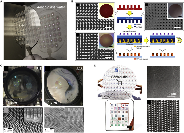
Figure 7.
Large-Scale Manufacturing of Metalenses
(A) Metalens array fabricated by using DUV lithography on a 4-inch glass wafer. Reprinted with permission from (Park et al., 2019). Copyright 2019, American Chemical Society.
(B) Fabrication schematic of the nanoparticle composite-based scalable one-step printing process. Scale bars, 1 μm. (insets) Optical micrographs of each. Scale bars, 100 μm. Reprinted with permission from (Yoon et al., 2020). Copyright 2020, Springer Nature.
(C) Comparison of metalens fabrication results using conventional reactive ion etching (RIE) and selective area sublimation (SAS) on a sapphire wafer. Reprinted with permission from (Brière et al., 2019). Copyright 2019, John Wiley & Sons.
(D) (left) Metalenses fabricated by using DUV lithography on a 12-inch glass wafer. (right) SEM images of the metalens. Reprinted with permission from (Hu et al., 2020). Copyright 2020, De Gruyter.

